Table of Contents
Advertisement
Quick Links
___________________________________________________________________________________________________________________
GS-EVB-DRG-100V7R-GS2
100 V Driver GaN Open Loop Buck/Boost Evaluation Board
Technical Manual
Visit
www.gansystems.com
WARNING:
PCB surface can become hot. Contact may cause burns. Do not touch!
CAUTION!
This product contains parts that are susceptible to damage by electrostatic discharge (ESD).
Always follow ESD prevention procedures when handling the product.
GS-EVB-DRG-100V7R-GS2 TM Rev. 201013
100 V Driver GaN Open Loop Buck/Boost
for the latest version of this technical manual.
© 2020 GaN Systems Inc.
Please refer to the Evaluation Board/Kit Important Notice on page 10
GS-EVB-DRG-100V7R-GS2
Evaluation Board Technical Manual
www.gansystems.com
1
Advertisement
Table of Contents

Related Manuals for Gan Systems GS-EVB-DRG-100V7R-GS2


Summary of Contents for Gan Systems GS-EVB-DRG-100V7R-GS2
- Page 1 CAUTION! This product contains parts that are susceptible to damage by electrostatic discharge (ESD). Always follow ESD prevention procedures when handling the product. GS-EVB-DRG-100V7R-GS2 TM Rev. 201013 © 2020 GaN Systems Inc. www.gansystems.com Please refer to the Evaluation Board/Kit Important Notice on page 10...
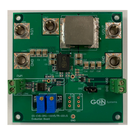
- Page 2 ___________________________________________________________________________________________________________________ Overview GS-EVB-DRG-100V7R-GS2 Evaluation Board with 100V DrGaN SMT power stage provides a complete 48V step down converter which can be used to evaluate efficiency & power density for use in applications such as CPU/GPU/DDR, high-performance Class D audio systems, and forward converters, ZVS, and buck / GS-EVB-DRG-100V7R-GS2 is intended and made available for testing and boost topologies.
-
Page 3: Electrical Specifications
Block Diagram and schematics 5V ~ 6V BOOT BOOT PHASE CLAMP PWM_H PWM_L PGND AGND Figure 1 DrGaN Module Block Diagram GS-EVB-DRG-100V7R-GS2 TM Rev. 201013 © 2020 GaN Systems Inc. www.gansystems.com Please refer to the Evaluation Board/Kit Important Notice on page 10... - Page 4 GS-EVB-DRG-100V7R-GS2 100 V Driver GaN Open Loop Buck/Boost Evaluation Board Technical Manual ___________________________________________________________________________________________________________________ Figure 2 Evaluation Board Schematics GS-EVB-DRG-100V7R-GS2 TM Rev. 201013 © 2020 GaN Systems Inc. www.gansystems.com Please refer to the Evaluation Board/Kit Important Notice on page 10...
-
Page 5: Pin Description
Board Setup Below is an example of board connection setup for 150W Open Loop Buck DC/DC Converter. Figure 4 Board Connection for Open Loop Buck DC/DC Converter GS-EVB-DRG-100V7R-GS2 TM Rev. 201013 © 2020 GaN Systems Inc. www.gansystems.com Please refer to the Evaluation Board/Kit Important Notice on page 10... -
Page 6: Test Results
Evaluation Board Technical Manual ___________________________________________________________________________________________________________________ Test Results Figure 5 Efficiency (not including driver loss Figure 6 Switching Waveform: F = 1 MHz GS-EVB-DRG-100V7R-GS2 TM Rev. 201013 © 2020 GaN Systems Inc. www.gansystems.com Please refer to the Evaluation Board/Kit Important Notice on page 10... -
Page 7: Bill Of Materials (Bom)
100 V Driver GaN Open Loop Buck/Boost Evaluation Board Technical Manual ___________________________________________________________________________________________________________________ Bill of Materials (BOM) Table 3 Bill of Materials GS-EVB-DRG-100V7R-GS2 TM Rev. 201013 © 2020 GaN Systems Inc. www.gansystems.com Please refer to the Evaluation Board/Kit Important Notice on page 10... -
Page 8: Pcb Layout
PCB Layout Figure 7 PCB Layout - Top Layer (L1) Figure 8 PCB Layout - Mid Layer 1 (L2) GS-EVB-DRG-100V7R-GS2 TM Rev. 201013 © 2020 GaN Systems Inc. www.gansystems.com Please refer to the Evaluation Board/Kit Important Notice on page 10... - Page 9 Evaluation Board Technical Manual ___________________________________________________________________________________________________________________ Figure 9 PCB Layout - Mid Layer 2 (L3) Figure 10 PCB Layout – Bottom Layer (L4) GS-EVB-DRG-100V7R-GS2 TM Rev. 201013 © 2020 GaN Systems Inc. www.gansystems.com Please refer to the Evaluation Board/Kit Important Notice on page 10...
- Page 10 The user assumes all responsibility and liability for proper and safe handling of the goods. Further, the user indemnifies GaN Systems from all claims arising from the handling or use of the goods. Due to the open construction of the product, it is the user’s responsibility to take any and all appropriate precautions with regard to electrostatic discharge.
- Page 11 The information given in this document shall not in any event be regarded as a guarantee of performance. GaN Systems hereby disclaims any or all warranties and liabilities of any kind, including but not limited to warranties of non-infringement of intellectual property rights.
- Page 12 Mouser Electronics Authorized Distributor Click to View Pricing, Inventory, Delivery & Lifecycle Information: GaN Systems GS-EVB-DRG-100V7R-GS2...
Need help?
Do you have a question about the GS-EVB-DRG-100V7R-GS2 and is the answer not in the manual?
Questions and answers