Table of Contents
Advertisement
Quick Links
GS61004B-EVBCD
GaN E-HEMT Full Bridge Evaluation Board
User's Guide
_____________________________________________________________________________________________________________________
GS61004B-EVBCD
100V GaN E-HEMT Full Bridge Evaluation
Board.
User's Guide
Visit
www.gansystems.com
for the latest version of this user's guide.
GS61004B-EVBCD Rev 200106
© 2020 GaN Systems Inc.
www.gansystems.com
1
Please refer to the Evaluation Board/Kit Important Notice on page 27
Advertisement
Table of Contents

Related Manuals for Gan Systems GS61004B-EVBCD


Summary of Contents for Gan Systems GS61004B-EVBCD
- Page 1 GS61004B-EVBCD 100V GaN E-HEMT Full Bridge Evaluation Board. User’s Guide Visit www.gansystems.com for the latest version of this user’s guide. GS61004B-EVBCD Rev 200106 © 2020 GaN Systems Inc. www.gansystems.com Please refer to the Evaluation Board/Kit Important Notice on page 27...
- Page 2 ESD prevention procedures when handling the product. Avoid applying excessive voltages to the power supply terminals or signal inputs or outputs GS61004B-EVBCD Rev 200106 © 2020 GaN Systems Inc. www.gansystems.com Please refer to the Evaluation Board/Kit Important Notice on page 27...
- Page 3 This user’s guide includes the evaluation board schematic, circuit description, a quick-start guide and measurement results. Evaluation Kit Contents and Requirements Kit Contents The GS61004B-EVBCD EVB includes the following hardware required to evaluate the GaN E- HEMT Driver. Table 1 GS61004B-EVBCD Evaluation Kit Contents...
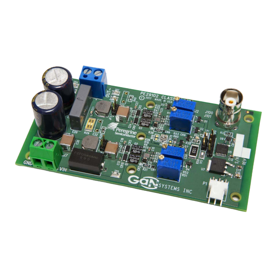
- Page 4 Probe points are included for waveform measurements. Provision has been made for a single, suitable heatsink to be fastened against the four E-HEMTs, using the three holes in the center of the board. Figure 1 • GS61004B-EVBCD Evaluation Board Assembly GS61004B-EVBCD Rev 200106 © 2020 GaN Systems Inc. www.gansystems.com...
- Page 5 The block diagram and schematic of the evaluation board are provided in Figures 2, 3, and 4, Figure 2 • PE29102 Full-Bridge EVB Block Diagram GS61004B-EVBCD Rev 200106 © 2020 GaN Systems Inc. www.gansystems.com Please refer to the Evaluation Board/Kit Important Notice on page 27...
- Page 6 PE29102 Full-Bridge EVB Schematic (1 of 2) Note: * CAUTION: Parts and assemblies susceptible to damage by electrostatic discharge (ESD). GS61004B-EVBCD Rev 200106 © 2020 GaN Systems Inc. www.gansystems.com Please refer to the Evaluation Board/Kit Important Notice on page 27...
- Page 7 PE29102 Full-Bridge EVB Schematic (2 of 2) Note: * CAUTION: Parts and assemblies susceptible to damage by electrostatic discharge (ESD). GS61004B-EVBCD Rev 200106 © 2020 GaN Systems Inc. www.gansystems.com Please refer to the Evaluation Board/Kit Important Notice on page 27...
-
Page 8: Circuit Description
A Zobel network (a.k.a. "Snubber" or "Boucheret Cell") may be connected from each switch node to ground to tame the high frequency response of the circuit when confronted with a complex reactive GS61004B-EVBCD Rev 200106 © 2020 GaN Systems Inc. www.gansystems.com Please refer to the Evaluation Board/Kit Important Notice on page 27... - Page 9 Figure 5 • PE29102 Dead-time Waveforms GS61004B-EVBCD Rev 200106 © 2020 GaN Systems Inc. www.gansystems.com Please refer to the Evaluation Board/Kit Important Notice on page 27...
- Page 10 GaN E-HEMT Full Bridge Evaluation Board User’s Guide _____________________________________________________________________________________________________________________ Figure 6 • Dead Time vs Dead Time Resistor RDLH RDHL GS61004B-EVBCD Rev 200106 © 2020 GaN Systems Inc. www.gansystems.com Please refer to the Evaluation Board/Kit Important Notice on page 27...
-
Page 11: Overcurrent Protection Circuit
R71 protects transistor Q7 from otherwise excessive transient discharge current from the shorting of capacitor C34, which could reach within 5V of the applied V IN voltage. GS61004B-EVBCD Rev 200106 © 2020 GaN Systems Inc. www.gansystems.com Please refer to the Evaluation Board/Kit Important Notice on page 27... - Page 12 ZXTP2027FTA 0.047µF 100V 0603 2512 EN<1> 1.8K ±5% 1/10W 0603 3.3K This page intentionally left blank. ±5% 1/10W 0603 SML-311UTT86 GS61004B-EVBCD Rev 200106 © 2020 GaN Systems Inc. www.gansystems.com Please refer to the Evaluation Board/Kit Important Notice on page 27...
-
Page 13: Evaluation Board Overview
User’s Guide _____________________________________________________________________________________________________________________ Quick Start Guide The GS61004B-EVBCD EVB is designed to ease customer evaluation of the PE29102 Full-Bridge E- HEMT Driver. This chapter will guide the user through the evaluation board overview, hardware operation, test setup and test results. - Page 14 DC “HV” Input: +12V to +30V DC “LV” Input: +8V to +24V On P1 Center Pin+, Outer Pins = GND GS61004B-EVBCD Rev 200106 © 2020 GaN Systems Inc. www.gansystems.com Please refer to the Evaluation Board/Kit Important Notice on page 27...
- Page 15 _____________________________________________________________________________________________________________________ Figure 9 • "XOR" Derived Phase Inversion Jumper Settings Figure 10 • Jumper Settings for PE29102 Derived Phase Inversion GS61004B-EVBCD Rev 200106 © 2020 GaN Systems Inc. www.gansystems.com Please refer to the Evaluation Board/Kit Important Notice on page 27...
- Page 16 GaN E-HEMT Full Bridge Evaluation Board User’s Guide _____________________________________________________________________________________________________________________ Figure 11 • Adjustments and Indicator Figure 12 • Test Points GS61004B-EVBCD Rev 200106 © 2020 GaN Systems Inc. www.gansystems.com Please refer to the Evaluation Board/Kit Important Notice on page 27...
-
Page 17: Hardware Operation
Apply the modulating PWM input signal. As switching frequency and output load increase, exercise care not to exceed the junction temperature of the devices. GS61004B-EVBCD Rev 200106 © 2020 GaN Systems Inc. www.gansystems.com Please refer to the Evaluation Board/Kit Important Notice on page 27... - Page 18 Full Bridge. A 50:50 square wave will produce the smallest output because each half of the bridge is modulated by an equal and opposite amount. GS61004B-EVBCD Rev 200106 © 2020 GaN Systems Inc. www.gansystems.com Please refer to the Evaluation Board/Kit Important Notice on page 27...
- Page 19 Adjust R68 until the LED DS-1 just extinguishes. The current limit now matches what you are loading TP5 with to ground. Power down and disconnect load. The board is now ready for use. GS61004B-EVBCD Rev 200106 © 2020 GaN Systems Inc. www.gansystems.com Please refer to the Evaluation Board/Kit Important Notice on page 27...
-
Page 20: Evaluation Results
The evaluation results are shown in Figures 14 to 16. Figure 14 • Oscilloscope Plot Showing Both SW Node Signals (Central Trace Shows PWM Input Signal) GS61004B-EVBCD Rev 200106 © 2020 GaN Systems Inc. www.gansystems.com Please refer to the Evaluation Board/Kit Important Notice on page 27... - Page 21 Audio 1 kHz Sine Wave Signal Recovered at Loudspeaker Output from a 200 kHz PWM Input Signal (Shown in the Background) GS61004B-EVBCD Rev 200106 © 2020 GaN Systems Inc. www.gansystems.com Please refer to the Evaluation Board/Kit Important Notice on page 27...
- Page 22 User’s Guide _____________________________________________________________________________________________________________________ Figure 16 • GS61004B-EVBCD Efficiency (%) Plotted Against Output Current (in A) with a 30V DC Supply and Output into an 8 Ohm Resistive Load, by Varying the Mark:Space Ratio of a 384 kHz PWM Signal GS61004B-EVBCD Rev 200106 ©...
-
Page 23: Thermal Considerations
Figure 17 • GS61004B-EVBCD EVB Thermal Plot Showing Maximum of 57 C with PWM 1.26 S Pulse Width at 200 kHz, with 30V @1 A on HV PSU into 8 Ohm Resistive Load With a 5:1 duty cycle corresponding to a near-maximum pulse width modulation index into a suitable load, the hottest components are the resistors in the Zobel/Snubber Networks (if/when fitted) and the inductors. - Page 24 The negative capacitor terminals should go to the + speaker connections, with the – speaker connections both going to Ground, preferably starred from Pin 1 J7, the DC power inlet ground terminal. GS61004B-EVBCD Rev 200106 © 2020 GaN Systems Inc. www.gansystems.com Please refer to the Evaluation Board/Kit Important Notice on page 27...
- Page 25 Connect the negative (-) end of each of these capacitors to the respective LS positive terminals. • Negative LS terminals connect to GND (see block diagram). • GS61004B-EVBCD Rev 200106 © 2020 GaN Systems Inc. www.gansystems.com Please refer to the Evaluation Board/Kit Important Notice on page 27...
-
Page 26: Technical Resources
Modified Block Diagram for Independent Dual (Stereo) Half-Bridge Topology Technical Resources This document and additional technical resources are available for download from www.gansystems.com. GS61004B-EVBCD Rev 200106 © 2020 GaN Systems Inc. www.gansystems.com Please refer to the Evaluation Board/Kit Important Notice on page 27... - Page 27 The user assumes all responsibility and liability for proper and safe handling of the goods. Further, the user indemnifies GaN Systems from all claims arising from the handling or use of the goods. Due to the open construction of the product, it is the user’s responsibility to take any and all appropriate precautions with regard to electrostatic discharge.
- Page 28 The information given in this document shall not in any event be regarded as a guarantee of performance. GaN Systems hereby disclaims any or all warranties and liabilities of any kind, including but not limited to warranties of non-infringement of intellectual property rights.
Need help?
Do you have a question about the GS61004B-EVBCD and is the answer not in the manual?
Questions and answers