Sign In
Upload
Manuals
Brands
Gan Systems Manuals
Motherboard
GS-EVB-HBDB-IMS
Gan Systems GS-EVB-HBDB-IMS Manuals
Manuals and User Guides for Gan Systems GS-EVB-HBDB-IMS. We have
1
Gan Systems GS-EVB-HBDB-IMS manual available for free PDF download: Technical Manual
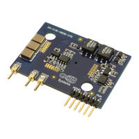
Gan Systems GS-EVB-HBDB-IMS Technical Manual (20 pages)
650 V Universal Half Bridge Isolated Driver Motherboard for IMS2 & IMS3
Brand:
Gan Systems
| Category:
Motherboard
| Size: 1 MB
Table of Contents
Table of Contents
3
Overview
5
Introduction
5
Features and Benefits
5
Applications
5
Content
5
Table 1 GS-EVB-IMS3-665Xxb-GS Evaluation Kit Contents
5
Figure 1 IMS EVB Motherboard GS-EVB-HBDB-IMS
6
Figure 2 Assembled IMS EVB Module with Heatsink
6
Motherboard Technical Specifications
7
Half Bridge Isolated Driver Mother Board Overview
7
Figure 3 Circuit Block Diagram of IMS EVB Module
7
Figure 4 Labelled Driver Motherboard
7
Gate Driver Circuit
8
Input and External PWM Signals Input
8
Figure 5 Gate Driver Circuit (Silicon Labs P/N: Si8271)
8
Figure 6 External 5V and PWM Signals Connector Pin
8
Temperature Monitoring Hole
9
Installation of IMS Half-Bridge Daughter Power Board
9
DC Link Decoupling Capacitors
9
Figure 7 Soldering Pin Guide
9
IMS Half Bridge Daughter Power Board Options
10
Figure 8 Cross-Section View of IMS Assembly Showing the Power Loop Path
10
Figure 9 Compatible IMS2 Daughter Power Boards
10
Table 2 Compatible IMS Daughter Power Board for Driver Motherboard GS-EVB-HBDB-IMS
10
Figure 10 Compatible IMS3 Daughter Power Boards
11
Figure 11 GS66516B and GS66508B Ganpx® Packaged Gan E-Mode Transistor
11
Figure 12 Cross-Section View of a Single Layer IMS Board
11
Test Results
12
Double Pulse Test (GS-EVB-HBDB-IMS + GS-EVB-IMS3-66508B-GS)
12
Figure 13 Double Pulse Test Setup Schematics
12
Table 3 Part Numbers and Description
12
Figure 14 Double Pulse Test Setup
13
Figure 15 Double Pulse Test Waveforms (400V/30A)
13
Boost Configuration Test (GS-EVB-HBDB-IMS + GS-EVB-IMS3-66508B-GS)
14
Figure 16 Boost Configuration Test Setup Schematics
14
Figure 17 Boost Configuration Test Setup
14
Figure 18 Boost Configuration Test Thermal Measurement Result
15
Figure 19 Test Waveforms (400Vin, 10Khz, Po=0.8Kw)
15
GS-EVB-HBDB-IMS Schematics and Bom
16
Advertisement
Advertisement
Related Products
Gan Systems GS-EVB-DRG-100V7R-GS2
Gan Systems GS665MB-EVB
GaN Systems GS66502B-EVBDB
GaN Systems GS66508B-EVBDB
GaN Systems GS66508T-EVBHB
GaN Systems GS65011-EVBEZ
Gan Systems GS61004B-EVBCD
Gan Systems GSWP050W-EVBPA
Gan Systems GSWP300W-EVBPA
Gan Systems GSP665HPMB-EVBIMS2
Gan Systems Categories
Motherboard
Switch
Control Unit
More Gan Systems Manuals
Login
Sign In
OR
Sign in with Facebook
Sign in with Google
Upload manual
Upload from disk
Upload from URL