Table of Contents
Advertisement
Quick Links
Advertisement
Table of Contents

Related Manuals for Freescale Semiconductor i.MX53


Summary of Contents for Freescale Semiconductor i.MX53
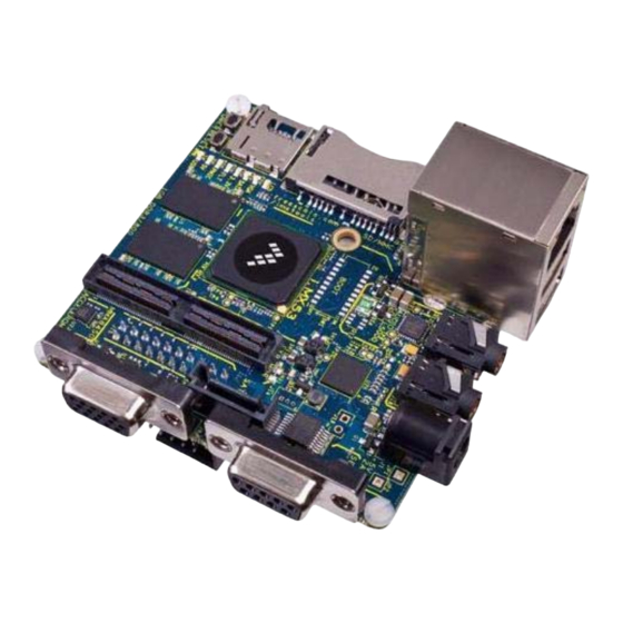
- Page 1 i.MX53 Quick Start Board Take your Multimedia freescale TM Experience to the max semiconductor Freescale Semiconductor Hardware User Guide for i.MX53 Quick Start Board, Preliminary Rev 0.91 PUBI – Public Use Business Information...
- Page 2 81829 Muenchen, Germany does Freescale Semiconductor assume any liability arising out of the application or +44 1296 380 456 (English) use of any product or circuit, and specifically disclaims any and all liability, including +46 8 52200080 (English) without limitation consequential or incidental damages.
-
Page 3: Table Of Contents
4. Quick Start Board Connectors and Expansion Port................ 15 4.1. Wall 5V Power Jack (J1) ....................... 16 4.2. RJ45 Ethernet Connector (J2B) .................... 17 4.3. VGA DB15 Connector (J8) ...................... 18 4.4. Debug UART DB9 Connector (J16) .................... 19 4.5. Headphone Output Connector (J18) ................... 20 4.6. Microphone Input Connector (J6) .................... 21 Freescale Semiconductor Hardware User Guide for i.MX53 Quick Start Board, Preliminary Rev 0.91 PUBI – Public Use Business Information... - Page 4 5.10. Expansion Port ........................ 56 5.11. Audio ............................ 57 5.12. Ethernet .......................... 58 5.13. USB Host connections ...................... 59 5.14. SATA ............................ 60 5.15. Debug UART Serial Port...................... 61 5.16. JTAG Operations ........................ 62 6. Connector Pin‐Outs .......................... 63 Freescale Semiconductor Hardware User Guide for i.MX53 Quick Start Board, Preliminary Rev 0.91 PUBI – Public Use Business Information...
- Page 5 PMIC Voltage Rail Test Points .................... 93 11. Known Issues ........................... 95 12. PCB Component Locations ...................... 96 13. Schematics ............................ 101 14. Bill of Materials .......................... 115 15. PCB information .......................... 122 Freescale Semiconductor Hardware User Guide for i.MX53 Quick Start Board, Preliminary Rev 0.91 PUBI – Public Use Business Information...
- Page 6 Expansion Port (J13) ……………………………………………………………………………………………….… 74 Figure 33. Optional HDMI Daughter Card…………………………………………………………………………………… 80 Figure 34. MCIMX28LCD 4.3” WVGA Display Daughter Card…………………………………………….………… 82 Figure 35. LVDS Display Kit………………………………………………………………………………………………………… 84 Figure 36. Quick Start Board Dimensions…………………………………………………………………………………… 86 Figure 37. Ethernet Loopback Cable………………………………………………………………………………………….. 91 Figure 38. Regulator Output Capacitor Positions Bottom………………………………………………………….. 93 Figure 39. Regulator Output Capacitor Positions Top………………………………………………………………… 94 Figure 40. Major Component Highlights Top…………………………………………………………………………….. 97 Freescale Semiconductor Hardware User Guide for i.MX53 Quick Start Board, Preliminary Rev 0.91 PUBI – Public Use Business Information...
- Page 7 Figure 62. Sixth Etch Layer………………………………………………………………………………………………………….128 Figure 63. Seventh Etch Layer……………………………………………………………………………………………………..129 Figure 64. Bottom Etch Layer………………………………………………………………………………………………………130 Figure 65. Soldermask Top………………………………………………………………………………………………………….131 Figure 66. Soldermask Bottom……………………………………………………………………………………………………132 Figure 67. Pastemask Top…………………………………………………………………………………………………………..133 Figure 68. Pastemask Bottom……………………………………………………………………………………………………..134 Figure 69. Silkscreen Top…………………………………………………………………………………………………………….135 Figure 70. Silkscreen Bottom………………………………………………………………………………………………………136 Freescale Semiconductor Hardware User Guide for i.MX53 Quick Start Board, Preliminary Rev 0.91 PUBI – Public Use Business Information...
- Page 8 Table 24. Debug UART Connector (J16) ……………………………………………………………………………………. 72 Table 25. JTAG Connector (J15) ……………………………………………………………………………………………….. 73 Table 26. Expansion Port (J13) …………………………………………………………………………………………………. 74 Table 27. Expansion Port Pin‐Mux Table……………………………………………………………………………………. 76 Table 28. Board Stack up information………………………………………………………………………………………… 87 Table 29. Problem Resolution Table………………………………………………………………………………………….. 92 Table 30. Output Capacitors and Values BOTTOM…………………………………………………………………….. 93 Table 31. Output Capacitors and Values TOP……………………………………………………………………………. 94 Freescale Semiconductor viii Hardware User Guide for i.MX53 Quick Start Board, Preliminary Rev 0.91 PUBI – Public Use Business Information...
-
Page 9: Introduction
Expansion Header: 120‐Pin Header (Populated) to Support 1 of the following: Optional HDMI Output Daughter Card (orderable) Optional WVGA and WQVGA LCD Display Daughter Cards (orderable) Camera Daughter Card (custom) SDIO Based WiFi Daughter card (custom) Freescale Semiconductor Hardware User Guide for i.MX53 Quick Start Board, Preliminary Rev 0.91 PUBI – Public Use Business Information... -
Page 10: 1.2. I.mx53-Quick Start Board Kit Contents
USB Cable (Standard‐A to Micro‐B connectors) 5V/2.0A Power Supply Quick Start Guide Documentation DVD 1.3. i.MX53 Quick Start Board Revision History Rev A – Proof of Concept Rev B – Prototype (Internal Freescale Development) Rev C – Prototype (Internal Freescale Development) Rev D – Production (Silicon: i.MX53 Rev 2.0, DA9053 Rev AA) Rev E – Production (Silicon: i.MX53 Rev 2.0, DA9053 Rev BB) The board assembly version will be printed on a label, usually attached to the side of the Ethernet/Dual USB Connector (J2). The assembly version will be the letter designation following the schematic revision: 700‐26565 REV _ Freescale Semiconductor Hardware User Guide for i.MX53 Quick Start Board, Preliminary Rev 0.91 PUBI – Public Use Business Information... -
Page 11: 2. List Of Acronyms
SSI ‐ Synchronous Serial Interface ULPI ‐ UTMI Low Pin Interface USB ‐ Universal Serial Bus UTMI ‐ Universal Transceiver Macrocell Interface WDOG ‐ Watch Dog WLAN ‐ Wireless LAN Freescale Semiconductor Hardware User Guide for i.MX53 Quick Start Board, Preliminary Rev 0.91 PUBI – Public Use Business Information... -
Page 12: Specifications
− TM Samsung One NAND and managed NAND including eMMC up to rev 4.4 (in muxed I/O mode) The i.MX53 system is built around the following system on chip interfaces: • 64‐bit AMBA AXI v1.0 bus – used by ARM platform, multimedia accelerators (such as VPU, IPU, GPU3D, GPU2D) and the external memory controller (EXTMC) operating at 200 MHz. • 32‐bit AMBA AHB 2.0 bus – used by the rest of the bus master peripherals operating at 133 MHz. • 32‐bit IP bus – peripheral bus used for control (and slow data traffic) of the most system peripheral devices operating at 66 MHz. The i.MX53 makes use of dedicated hardware accelerators to achieve state‐of‐the‐art multimedia performance. The use of hardware accelerators provides both high performance and low power consumption while freeing up the CPU core for other tasks. Freescale Semiconductor Hardware User Guide for i.MX53 Quick Start Board, Preliminary Rev 0.91 PUBI – Public Use Business Information... - Page 13 Camera sensors: − Two parallel 20‐bit camera ports. Primary up to 180‐MHz peak clock frequency, secondary up to 120‐MHz peak clock frequency. • Expansion cards: − Four SD/MMC card ports: three supporting 416 Mbps (8‐bit i/f) and one enhanced port supporting 832 Mbps (8‐bit, eMMC 4.4) • USB − High‐speed (HS) USB 2.0 OTG (up to 480 Mbps), with integrated HS USB PHY − Three USB 2.0 (480 Mbps) hosts: High‐speed host with integrated on‐chip high speed PHY Two high‐speed hosts for external HS/FS transceivers through ULPI/serial, support IC‐USB Freescale Semiconductor Hardware User Guide for i.MX53 Quick Start Board, Preliminary Rev 0.91 PUBI – Public Use Business Information...
- Page 14 • Secure real‐time clock (SRTC) – Tamper resistant RTC with dedicated power domain and mechanism to detect voltage and clock glitches. • Real‐time integrity checker, version 3 (RTICv3) – RTIC type 1, enhanced with SHA‐256 engine • SAHARAv4 Lite – Cryptographic accelerator that includes true random number generator (TRNG) • Security controller, version 2 (SCCv2) – Improved SCC with AES engine, secure/nonsecure RAM and support for multiple keys as well as TZ/non‐TZ separation. • Central Security Unit (CSU) – Enhancement for the IIM (IC Identification Module). CSU is configured during boot and by e‐fuses and determines the security level operation mode as well as the TrustZone (TZ) policy. • Advanced High Assurance BOOT (A‐HAB) – HAB with the next embedded enhancements: SHA‐256, 2046‐bit RSA key, version control mechanism, warm boot, CSU and TZ initialization. Freescale Semiconductor Hardware User Guide for i.MX53 Quick Start Board, Preliminary Rev 0.91 PUBI – Public Use Business Information...
-
Page 15: 3.2. Ddr3 Dram Memory
1 for the ARM Core supply (VBUCKCORE) 1 for the Peripheral Core supply (VBUCKPRO) 1 for the external SDRAM memory (VBUCKMEM) 1 for the internal cache memory (VBUCKPERI) o 1 White LED driver and boost converter • Li‐ION battery Charger • Resistive touch screen interface • Expansion Port Card ID detect • Wall voltage supply over‐voltage protection • 1 HS‐I2C interface • External LDO regulator enable Freescale Semiconductor Hardware User Guide for i.MX53 Quick Start Board, Preliminary Rev 0.91 PUBI – Public Use Business Information... -
Page 16: Microsd Card Slot (J4)
3.6. SATA 7‐pin Data Connector (J7) The SATA connector provides the means to connect an external SATA memory device to the Quick Start board. Commonly, this would be an External hard drive or a DVD/CD reader. Power for the SATA device needs to be supplied externally by the user via a 12‐pin power connector. It is possible to boot from a SATA drive by making OTP fuse changes. Once the fuse changes are made, they cannot be reversed. 3.7. VGA Video Output (J8) A standard VGA signal is output directly from the i.MX53 Processor with minimum external components required. Power for the TVE module of the i.MX535 Processor is supplied by VLDO7 of the PMIC and is set to 2.75V. If VGA output is not desired, it is possible to program the PMIC to turn off VLDO7 to conserve power. The VGA output supports a variety of video formats up to 150 Mega‐Pixels per second. Level shifters are required on the Horizontal and Vertical Synchronization signals as well as the VGA I2C communications signals in order to meet VGA specifications. Freescale Semiconductor Hardware User Guide for i.MX53 Quick Start Board, Preliminary Rev 0.91 PUBI – Public Use Business Information... -
Page 17: Lvds Video Output (J9)
3.10. Dual USB Host Connector (J2A) The USB module of the i.MX53 Processor provides two high speed USB PHYs that are connected to each of the USB‐A Host Jacks on connector J2. One PHY provides Host‐only functionality and is connected to the upper USB jack on the connector tower. The second PHY is USB 2.0 OTG capable and is connected to the lower USB jack on the connector tower. Both jacks receive 5V power directly from the 5V Wall Power Supply, via a FET that can be controlled by software, and a 1.1A Poly‐fuse. The PMIC provides an over‐voltage functionality to limit voltage applied to the USB jack in the event that a DC Power Supply other than the original supply provided is used. Also, there is no current regulating device to limit current supplied to each jack, other than the Poly‐fuse. NOTE The lower USB Host Jack is cross connected with the Micro‐B USB Device connector. This was done as a convenience to the user as cables with micro‐A plugs are still uncommon at the time the board was designed. The USB OTG PHY will switch to ‘device’ mode if a USB Host is attached to the micro‐B connector with a cable. This design is not recommended for release to the general electronics consumer population. This board has not been tested for USB compliance. Freescale Semiconductor Hardware User Guide for i.MX53 Quick Start Board, Preliminary Rev 0.91 PUBI – Public Use Business Information... -
Page 18: Micro-B Usb Device Connector (J3)
Microphone Jack. A 2.5mm to 3.5mm adapter may be necessary to convert the microphone, mono headphone device to fit the Microphone Jack. On both the Headphone Jack and Microphone jack, a fourth pin is used to detect the insertion of a plug into either jack. When a standard 3‐pin device is inserted into the 4‐pin jack, the detect line is grounded, indicating to the i.MX53 Processor that the plug has been inserted. 3.13. 5V Power Connector (J1) A 2.0mm x 6.5mm barrel connector is used which should fit standard DC Plugs with an inner dimension of 2.1mm and an outer dimension of 5.5mm. If an alternate power supply is used (not the original, supplied power supply), it should supply no more than 5.25V / 3A output. If the PMIC senses too high voltage at the connector input, it will turn off isolation FET Q1 to protect the Quick Start board. In between the Power Connector and the isolation FET is a single blow, fast acting fuse to protect the Quick Start board from an over current situation fault. If a Wall Power Supply is properly connected to the Quick Start board, and the green 5V power LED indicator is not lit, it could mean that either the fuse has been blown, or that the voltage output of the power supply is too high. Freescale Semiconductor Hardware User Guide for i.MX53 Quick Start Board, Preliminary Rev 0.91 PUBI – Public Use Business Information... -
Page 19: Debug Uart Connector (J16)
3.15. JTAG Connector (J15) A standard 20‐pin ARM JTAG connector is provided on the Quick Start board. Logic signals to the JTAG connector are 1.8V signals. A 1.8V reference signal is provided to pin 1 of the connector so that the attached JTAG tool can automatically configure the logic signals for the right voltage. If the JTAG tool does not have an automatic logic voltage sense, make sure that the tool is configured for 1.8V logic. JTAG tools that have been specifically tested with the Quick Start board are: • JTAG Commander (Macraigor) • DS‐5 and RealView (ARM Ltd.) • Trace32 (Lauterbach) • J‐Link (Segger/Codesourcery) • J‐Link (IAR) Freescale Semiconductor Hardware User Guide for i.MX53 Quick Start Board, Preliminary Rev 0.91 PUBI – Public Use Business Information... -
Page 20: Expansion Header (J13)
User Interface Buttons There are four user interface buttons on the Quick Start board. Their functionality is as follows: POWER: In the ‘Power Off’ state, momentarily pressing the POWER button will begin the PMIC power on cycle. The PMIC supplied voltage rails will come up in the proper sequence to power the i.MX53 Processor. When the processor is fully powered, the boot cycle will be initiated. In the ‘Power On’ state, momentarily pressing the POWER button will send a signal to a GPIO port for user defined action, but will not initiate a hardware shutdown. In the ‘Power On’ state, holding the power button down for greater than 5 seconds will result in the PMIC initiating a shutdown to the ‘Standby’ power condition. This will also be the result from the ‘Power Off’ state as the PMIC will transition into the ‘Power On’ state and will still see the POWER button as held down. Freescale Semiconductor Hardware User Guide for i.MX53 Quick Start Board, Preliminary Rev 0.91 PUBI – Public Use Business Information... -
Page 21: 3.18. User Interface Led Indicators
The User status LED (D16) is a Green LED gated by the PATA_DATA1 (L3) GPIO pin. The developer is left to determine the action of this pin in code. Sample codes do not assign functionality to the pin. The LED comes on by default when the processor starts up. FLT: The FLT status LED (D14) is a Red LED gated by the NVDD_FAULT signal from the PMIC. The LED will turn on anytime the PMIC is not outputting the requested voltages or when the PMIC senses a fault condition and will begin to power down the voltage rails. This may aid in trouble shooting power problems if both the PMIC and FLT LEDs are on at the same time, it indicates that the PMIC is causing a shutdown based on a fault it has sensed. 3.3V: The 3.3V status LED (D10) is a Blue LED gated by the External Regulator 3.2V power rail. This power rail can be turned off by software for power savings measures. This LED provides an easy visual recognition as to the status of this bus. Freescale Semiconductor Hardware User Guide for i.MX53 Quick Start Board, Preliminary Rev 0.91 PUBI – Public Use Business Information... -
Page 22: Optional Li-Ion Batter Connector (J14)
The battery charging feature is an autonomous operation of the Dialog DA9053 PMIC that does not require software support. Battery charging may be prevented by software by making registry changes to the PMIC. The developer may need to verify in software that PMIC registry settings are proper for battery charging operations. The footprints for testing with a battery were included for skilled developers looking to experiment. 3.20. Optional Back‐Up Coin Cell posts (JP1, JP2) On the Quick Start board, there are two through‐holes (JP1 and JP2) next to the power connector. These through‐holes are positioned to hold a Lithium coin cell battery (Sanyo ML1220‐VM1 or equivalent). For proper operation, the coin cell posts should be soldered direction to the Quick Start board, with the positive terminal connected to JP1 and the negative terminal connected to JP2. The DA9053 PMIC will charge the coin cell when 5V Wall Power is available. When 5V Wall Power is removed, the coin cell will provide power only to the RTC power rail (VLDO1) supplying power to the i.MX53 processor. The length of time a coin cell can power the RTC subsystem may vary. Freescale Semiconductor Hardware User Guide for i.MX53 Quick Start Board, Preliminary Rev 0.91 PUBI – Public Use Business Information... -
Page 23: 3.21. Pcb Shorting Traces
1) Isolate power to major subsystems or components. 2) Install small value precision resistors to measure current consumption of major subsystems. 3) Or reconfigure power sources to subsystems or components using wires soldered to the pads. To restore a shorting trace back to normal after the trace is cut, it is only necessary to solder a Zero Ohm resistor to the pads. 4. Quick Start Board Connectors and Expansion Port The Quick Start board provides a number of connectors for a variety of inputs and outputs to and from the board. The following subsections describe these connections in detail. Freescale Semiconductor Hardware User Guide for i.MX53 Quick Start Board, Preliminary Rev 0.91 PUBI – Public Use Business Information... -
Page 24: Wall 5V Power Jack (J1)
(J1) on the board as show in Figure 1. If the original power supply is lost, it is possible to use a substitute power supply for the Quick Start board. Voltage above 5.5V, and below 12V, will trigger the Over‐ Voltage protection circuitry on the board. It is not recommended to use a higher voltage since, in the event of a failure to the protection circuitry, damage to the board will result. A voltage supply above 12V will damage the PMIC part. Power Jack (J1) Figure 1. DC Power Jack Freescale Semiconductor Hardware User Guide for i.MX53 Quick Start Board, Preliminary Rev 0.91 PUBI – Public Use Business Information... -
Page 25: Rj45 Ethernet Connector (J2B)
Figure 2a. Ethernet Port Figure 2. RJ45 Ethernet Connector Freescale Semiconductor Hardware User Guide for i.MX53 Quick Start Board, Preliminary Rev 0.91 PUBI – Public Use Business Information... -
Page 26: Vga Db15 Connector (J8)
4.3. VGA DB15 Connector (J8) To connect the Quick Start board to a computer monitor in the base configuration, a VGA cable is required. Connect the free end of the VGA cable to connector J8 to the point shown in Figure 3. VGA DB15 Connector (J8) Figure 3. VGA Connector Freescale Semiconductor Hardware User Guide for i.MX53 Quick Start Board, Preliminary Rev 0.91 PUBI – Public Use Business Information... -
Page 27: Debug Uart Db9 Connector (J16)
Connector (J16) Figure 4. Debug UART Connector Freescale Semiconductor Hardware User Guide for i.MX53 Quick Start Board, Preliminary Rev 0.91 PUBI – Public Use Business Information... -
Page 28: Headphone Output Connector (J18)
Figure 5. Headphone Output Connector Freescale Semiconductor Hardware User Guide for i.MX53 Quick Start Board, Preliminary Rev 0.91 PUBI – Public Use Business Information... -
Page 29: Microphone Input Connector (J6)
Figure 6. Microphone Connector (J6) Freescale Semiconductor Hardware User Guide for i.MX53 Quick Start Board, Preliminary Rev 0.91 PUBI – Public Use Business Information... -
Page 30: Dual Usb Host Connectors (J2)
Upper Lower Figure 7a. USB Connectors Figure 7. Dual USB Host Connectors (J2) Freescale Semiconductor Hardware User Guide for i.MX53 Quick Start Board, Preliminary Rev 0.91 PUBI – Public Use Business Information... -
Page 31: Micro-B Usb Device Connector (J3)
4.8. micro‐B USB Device Connector (J3) The Quick Start board has one micro‐B USB device connector that can be used to connect the Quick Start board to a USB Host computer. The micro‐B connector is connected to the High‐speed (HS) USB 2.0 OTG module of the i.MX53 processor and is cross connected with the lower USB Host port on J2. When a 5V supply is seen on the micro‐B connector (from the USB Host), the i.MX53 processor will configure the OTG module for device mode, which will prevent the lower USB Host port from operating correctly. The 5V power provided by the attached USB Host is only used by the i.MX53 processor for sensing that the host is present. The Quick Start board will not draw power from the connected USB Host and will not operate without a 5V DC power source or charged Li‐ION battery. The micro‐B connector is keyed and will not accept a micro‐A plug from a cable. A micro‐B to USB‐A cable is supplied as part of the Quick Start kit and can be inserted into the micro‐B USB connector at the point shown in Figure 8. micro‐B USB Connector (J3) Figure 8. micro‐B USB Device Connector (J3) Freescale Semiconductor Hardware User Guide for i.MX53 Quick Start Board, Preliminary Rev 0.91 PUBI – Public Use Business Information... -
Page 32: Sata Data Connector (J7)
It is possible to initiate a boot from an attached SATA device. See the software reference manuals for instructions on how to configure the Quick Start board for SATA boot. The SATA Data cable is plugged into the Quick Start board at the location shown in Figure 9. SATA 7‐pin Data Connector (J7) Figure 9. SATA Data Connector (J7) Freescale Semiconductor Hardware User Guide for i.MX53 Quick Start Board, Preliminary Rev 0.91 PUBI – Public Use Business Information... -
Page 33: Sd Card Connector (J5)
4.10. SD Card Connector (J5) The Quick Start board has one full size SD/MMC connector that can be used for memory, or for third‐ party SDIO type cards such as WiFi or Bluetooth. The SD Card Connector (J5) connects a full 8‐bit parallel data bus to the SD3 port of the i.MX53 processor. The SD Card Connector receives power from the DCDC_3V2 power rail supplied by the supplementary Voltage Regulator. The Quick Start board does not come pre‐configured to boot from the full size SD Card Connector, but the board can be modified to support booting from this connector instead of the microSD Card Connector. See the section on Quick Start boot options on how to make the necessary changes (Section 5.4.2). The SD Card Connector is not spring loaded, so pushing the card into the slot will not initiate an action to disengage the SD Card. The SD Card is inserted facing up at the location shown in Figure 10. SD Card Connector (J5) Figure 10. SD Card Connector (J5) Freescale Semiconductor Hardware User Guide for i.MX53 Quick Start Board, Preliminary Rev 0.91 PUBI – Public Use Business Information... -
Page 34: Microsd Card Connector (J4)
4.11. microSD Card Connector (J4) The Quick Start board has one micro SD/MMC connector that can be used for memory. The micro SD Card Connector (J4) connects a 4‐bit parallel data bus to the SD1 port of the i.MX53 processor. The micro SD Card Connector receives power from the VLDO3 power rail. The Quick Start board comes configured to boot from the micro SD Card Connector by default. The micro SD Card Connector is spring loaded and will eject a properly inserted card if the card is pushed in again. Caution: If the card is ejected while serving as the file system, the processor will undergo a software crash. The micro SD Card is inserted facing up at the location shown in Figure 11. microSD Connector (J4) Figure 11. microSD Card Connector (J4) Freescale Semiconductor Hardware User Guide for i.MX53 Quick Start Board, Preliminary Rev 0.91 PUBI – Public Use Business Information... -
Page 35: Jtag Connector (J15)
4.12. 20‐pin ARM JTAG Connector (J15) The Quick Start board contains a standard 20‐pin ARM JTAG connector (J15) for advanced debugging with a third‐party emulator. The header is configured for use with 1.8V data signals. The developer should exercise caution when selecting the appropriate debugging tools. If an emulator set for 3.3V power and data is connected to the Quick Start board, the i.MX53 processor will be damaged. The emulator JTAG cable is connected to the bottom side of the Quick Start board at the location shown in Figure 12. VGA DB15 Connector (J8) JTAG Connector (J15) Figure 12. JTAG Connector (J15) Freescale Semiconductor Hardware User Guide for i.MX53 Quick Start Board, Preliminary Rev 0.91 PUBI – Public Use Business Information... -
Page 36: Ldvs Connector (J9)
The Quick Start board includes a 30‐pin (Hirose, DF19G‐30P‐1H(56)) connector for use with an LVDS display. The developer can create custom cables that will allow the Quick Start board to be used with a wide variety of commercially available LVDS displays. The pin‐out for this connector is used on other Freescale designed boards in the i.MX53 series, such as the MCIMX53SMD tablet. Freescale has available a cable and LVDS display (HannStar, HSD100PXN1‐A00‐C11) for purchase if the developer wishes to use a pre‐tested configuration. The LVDS display can be used in conjunction with the optional LCD display, the VGA output or the optional HDMI card, as long as the total video output does not exceed the specified limits of the i.MX53 processor. The pin‐out table for the connector is located in different section of this user guide. This connector is located on the bottom side of the board in the location shown in Figure 13. LDVS Connector (J9) Figure 13. LDVS Connector (J9) Freescale Semiconductor Hardware User Guide for i.MX53 Quick Start Board, Preliminary Rev 0.91 PUBI – Public Use Business Information... - Page 37 Figure 14. i.MX53 Smart‐Start Block Diagram Freescale Semiconductor Hardware User Guide for i.MX53 Quick Start Board, Preliminary Rev 0.91 PUBI – Public Use Business Information...
-
Page 38: Board Main Power Circuit
Figure 15. Board Main Power Circuit. Freescale Semiconductor Hardware User Guide for i.MX53 Quick Start Board, Preliminary Rev 0.91 PUBI – Public Use Business Information... - Page 39 The power sequence requirements for the i.MX53 Applications Processor from the data sheet are as follows: NVCC_SRTC_POW (VLDO1) VCC, VDDA, VDDGP, VDD_REG [in any order] All other supplies [in any order] NOTE: in case the internal regulator is used for VDDA generation, the VDD_REG should be powered up together with VCC and VDDGP, before the other supplies. In case the internal regulator is not used to generate VDDA (as on the Quick Start board), the VDD_REG is independent and has no power‐up restrictions. The power on timing sequence shown in Table 1 is the sequence programmed into the Dialog PMIC. It is one way of providing sequences power to the i.MX53 processor. Designers are free to change the power timing sequence on their own board designs as long as the timing requirements are met. Freescale has not formally tested other power on timing sequences. Freescale Semiconductor Hardware User Guide for i.MX53 Quick Start Board, Preliminary Rev 0.91 PUBI – Public Use Business Information...
-
Page 40: Regulator Timing Sequence
Table 1. Regulator Timing Sequence The Dialog PMIC will enter a SHUTDOWN/STANDBY condition by one of three ways; By a command from the i.MX53 Processor via I2C communications, by i.MX53 Processor action to hold the nONKEY/KEEPACT pin low for at least five seconds, or by hardware if the user holds down the POWER button for more than five seconds. All three actions result in the Dialog PMIC powering down the voltage regulators in reverse order of the power on sequence, except for VLDO1. A subsequent press of the POWER button will initiate the same power on sequence as shown in Table 1. The various power rails supplied by the PMIC are discussed in the section on Quick Start Power Rails. Other features of the Dialog PMIC implemented by the Quick Start board are discussed in subsequent sub‐sections including: Li‐ION Battery Charging, Backlight LED Driver, Touch‐Screen Operation, Miscellaneous. Freescale Semiconductor Hardware User Guide for i.MX53 Quick Start Board, Preliminary Rev 0.91 PUBI – Public Use Business Information... -
Page 41: Quick Start Board Power Supply Rails
DIG_PLL_1V3 ALTERNATE FOR: DIG_PLL VLDO3 3.3V VLDO3_3V3 SD1_3V3 MICROSD CARD (SD1) I2C1/I2C2 BOOT_SEL NVCC‐EIM‐MAIN NVCC_EIM_SEC NVCC_SD1&2 NVCC_PATA NVCC_FEC NVCC_GPIO NVCC_KEYPAD Table 2. Quick Start Board Power Supply Rails Freescale Semiconductor Hardware User Guide for i.MX53 Quick Start Board, Preliminary Rev 0.91 PUBI – Public Use Business Information... - Page 42 VDDA_1V3 DCDC‐3V2 3.2V DCDC‐3V2 ETHERNET AUDIO_3V2 AUDIO FEC_3V2 VGA_IO_SIGNALS VDD_FUSE USB 3.3V LCD_3V2 SD CARD (SD3) EXPANSION PORT Table 2. Quick Start Board Power Supply Rails (con) Freescale Semiconductor Hardware User Guide for i.MX53 Quick Start Board, Preliminary Rev 0.91 PUBI – Public Use Business Information...
- Page 43 In designing a board using the Dialog PMIC, it is important to include a capacitor of 47 uF or greater attached to the VBAT pin if any operations are planned without a Li‐ION battery. If during the initial pre‐ charge phase, the Dialog PMIC does not sense any voltage present when the pre‐charge voltage is momentarily removed and VBAT voltage is measured, the PMIC will assume a massive board failure and will not supply any voltage via the regulators. 5.2.3. Backlight LED Driver The Dialog PMIC provides a Boost circuit which controls an external MOSFET Q8. The PMIC is capable of driving 3 independent strings of up to 5 white LEDs each with a voltage of approximately 24 Volts and a maximum of 50 mA. The Quick Start board does not have a direct connection for white backlight LEDs, but does supply one connection to the Expansion Port that can be used to support an attached LCD Daughter Card. The Expansion Port uses the LED1_IN port of the PMIC. Freescale Semiconductor Hardware User Guide for i.MX53 Quick Start Board, Preliminary Rev 0.91 PUBI – Public Use Business Information...
- Page 44 5.2.5. Miscellaneous If a coin cell battery is attached to the Quick Start board, it will automatically charge using the programmed charging settings whenever wall power is supplied to the Quick Start board. When the battery voltage reaches the programmed level, charging will stop. Battery discharge will not begin until wall power is removed from the board and, if a Li‐ION battery is attached, the main battery discharges to the battery cut off level. There are two port ID traces connected from the Expansion Port header to two of the ADC pins of the PMIC. Each unique Daughter Card designed by Freescale has a different resistor value attached to the two ID traces on the Daughter Card. It is possible to use this voltage divider identification system to determine at boot time if a daughter card is attached, and if so, which specific daughter card it is. Resistor values for the two daughter cards commonly used with the Quick start board are shown in Table 3. Freescale Semiconductor Hardware User Guide for i.MX53 Quick Start Board, Preliminary Rev 0.91 PUBI – Public Use Business Information...
-
Page 45: Port Id Resistor Values
The PMIC has several different options for Pull‐Up levels on each of its output pins. In some cases, VDDOUT is one option, along with power supplied to both the VDD_IO1 (L4) and VDD_IO2 (K4) pins as Pull‐Up source. The exact source of Pull‐Up power is determined by the registry settings of the PMIC and can be pre‐programmed at the factory as the designer wishes. Some Pull‐Up registry settings apply to groups of pins, so care must be made in selecting which source power source is used for a particular grouping of pins. The Dialog PMIC Datasheet contains much more detailed information on the registry settings. For the Quick Start board, VLDO3 (3.3V) is connected to VDD_IO1 primarily to ensure that the 3V3_EN signal sent to the external regulator is sufficient to turn on the regulator, and VLDO8 (1.8V) is connected to VDD_IO2 to provide for proper I2C TTL logic levels. Freescale Semiconductor Hardware User Guide for i.MX53 Quick Start Board, Preliminary Rev 0.91 PUBI – Public Use Business Information... - Page 46 Expansion Port (HDMI) 30 mA SD Card 60 mA For the Expansion Port and the SD Card socket, it may be that the current draws exceed the above estimates if a custom designed board is added to the Expansion Port, or if an SDIO device is plugged into the SD Card Socket (ie, WiFi, Bluetooth). The external voltage regulator is capable of supplying up to 1A of current and should be capable of accommodating most custom configurations. Since the Quick Start board was originally designed, it has been found that VDDA, VDDAL, and DIG_PLL can all be powered internally by the i.MX53 processor (with the correct eFuse settings). This would then free the PMIC VLDO2, VLDO6 and VLDO10 power sources for other uses. VLDO6 and VLDO10 will be able to supply the above expected loads, provided a high current draw SDIO card is not inserted in the SD Card Socket. The designer is free to rearrange power rails as desired. Freescale Semiconductor Hardware User Guide for i.MX53 Quick Start Board, Preliminary Rev 0.91 PUBI – Public Use Business Information...
- Page 47 5.4.1. Peripheral Module Logic Voltage Levels By convention, pins used on the I.MX53 Processor to set module logic voltage levels begin with NVCC_. This is to aid the developer in the design of a project based on the i.MX53 Processor. There are 25 such pins used, and practically speaking, they supply the internal pull‐up voltages for pins designated for data output. These 25 pins are shown in detail in Table 4. Module Voltage Supplies. Once a voltage level is selected for a particular module, all pins within that module will use the same voltage level. It is important for the developer not to try to use an external pull‐up to a different voltage level for individual pins. Level shifters must be used if certain pins need to have different voltage levels to interface with external ICs. If a different voltage level is used on an external pull‐up, one or both of the affected power rails will most likely have a different voltage level than intended throughout the design. On a newly designed board that shows unexpected voltage levels, this may be the first thing to check. On the Quick Start board, there are a number of unpopulated pull‐up resistors. This is a result of the initial design being conservative, and the addition of external pull‐up resistors to supplement internal i.MX53 pull‐up supply voltage. Subsequent Quick Start board usage has shown these pull‐ups to be unnecessary, so they are unpopulated. Freescale Semiconductor Hardware User Guide for i.MX53 Quick Start Board, Preliminary Rev 0.91 PUBI – Public Use Business Information...
- Page 48 LVDS Band Gap 2.375V ‐ 2.625V 2.5V Table 4. Module Voltage Supplies Freescale Semiconductor Hardware User Guide for i.MX53 Quick Start Board, Preliminary Rev 0.91 PUBI – Public Use Business Information...
-
Page 49: Boot_Mode Pin Settings
EIM_EB0 EIM_EB1 EIM_DA0 EIM_DA1 EIM_DA2 EIM_DA3 N/A N/A Default 0 0 1 1 1 0 ‐ ‐ Table 6B. BOOT_CFG Word2 Freescale Semiconductor Hardware User Guide for i.MX53 Quick Start Board, Preliminary Rev 0.91 PUBI – Public Use Business Information... -
Page 50: Table 6C
0000 ‐ NOR/OneNAND Boot 0001 ‐ Reserved 0010 ‐ PATA/SATA Boot 0011 ‐ Serial ROM (I2C/SPI) Boot 01XX ‐ SD/MMC (eSD/eMMC) Boot 1XXX ‐ NAND Flash Boot For each of the bootable source selections, the remaining BOOT_CFG pins have different meanings. The pins are meant to choose initialization settings required for each specific boot source. The following paragraphs will specify those choices base by bootable source: Freescale Semiconductor Hardware User Guide for i.MX53 Quick Start Board, Preliminary Rev 0.91 PUBI – Public Use Business Information... - Page 51 01 – CS1 10 – CS2 11 – CS3 Freescale Semiconductor Hardware User Guide for i.MX53 Quick Start Board, Preliminary Rev 0.91 PUBI – Public Use Business Information...
- Page 52 1 – Use eFUSE DLL Override BOOT_CFG3[2] Fast Boot Acknowledge 0 – Enabled 1 – Disabled Freescale Semiconductor Hardware User Guide for i.MX53 Quick Start Board, Preliminary Rev 0.91 PUBI – Public Use Business Information...
- Page 53 01 – 64 Pages 10 – 128 Pages 11 – 256 Pages Freescale Semiconductor Hardware User Guide for i.MX53 Quick Start Board, Preliminary Rev 0.91 PUBI – Public Use Business Information...
-
Page 54: Boot Mode Resistor Locations Top
Resistor Boot Configuration Bit Pull UP/Down R46 BOOT_CGF1[6] Pull Up R47 BOOT_CGF1[7] Pull Down R48 BOOT_CGF2[7] Pull Up (DNP) Table 7. Boot Mode Resistors TOP Freescale Semiconductor Hardware User Guide for i.MX53 Quick Start Board, Preliminary Rev 0.91 PUBI – Public Use Business Information... -
Page 55: Boot Mode Resistor Locations Bottom
Pull Up R60 BOOT_CGF2[5] Pull Up R61 BOOT_CGF2[4] Pull Up R59 BOOT_CGF2[6] Pull Down Table 8. Boot Mode Resistors BOTTOM Freescale Semiconductor Hardware User Guide for i.MX53 Quick Start Board, Preliminary Rev 0.91 PUBI – Public Use Business Information... - Page 56 Figure 18. Clock Source Locations The clock source for the Ethernet PHY is a 50 MHz Oscillator (X1) with an enable pin and is shown in Figure 18. The oscillator was originally placed to support both the SATA module and the Ethernet PHY. It is no longer used for the SATA module, and only supplies a clock signal to the Ethernet PHY. It is powered by the DCDC_3V2 power rail and, by default, is always on when the DCDC_3V2 rail is powered on. It is possible for the developer to remove resistor R110 and place a zero Ohm resistor across R197 to give the developer software control of the oscillator through pin GPIO_4 (D4). Freescale Semiconductor Hardware User Guide for i.MX53 Quick Start Board, Preliminary Rev 0.91 PUBI – Public Use Business Information...
- Page 57 5.4.5. Watch Dog Timer The i.MX53 Application Processor has an internal Watch Dog Timer circuit. On the Quick Start board, the WDOG output is assigned to GPIO_9. The WDOG is an active low signal. The Dialog PMIC does not have a specific pin to accept a Watch Dog signal to force a Processor reset. Therefore, the WDOG signal is modified by hardware components on the Quick Start board and applied to the Processor Reset pin (POR_B, pin C19). By using an active‐low enabled buffer, the active low WDOG signal can be transformed into a low pulse, which returns back to the logic high state immediately after the i.MX53 Processor resets ( ~ 700 nsec). This allows the processor to reset the WDOG signal and then come out of reset. The buffer IC also is in a tri‐state condition when the WDOG signal is normally high, thus allowing the push‐button reset circuitry to work. The Watch Dog circuitry is shown in Figure 19. Freescale Semiconductor Hardware User Guide for i.MX53 Quick Start Board, Preliminary Rev 0.91 PUBI – Public Use Business Information...
- Page 58 5.4.6. Wakeup After User Initiated Standby Q13 is a dual P‐channel/N‐channel MOSFET designed to take a transition from a low state to a high state on PMIC_ON_REQ (pin W15) and turn it into a PMIC nONKEY request to bring the Dialog DA9053 chip out of a standby state to a fully on state. The PMIC_ON_REQ pin has been designed to work with the Freescale companion PMIC chip and is always in a high state even if the user forces the board into standby with the nONKEY. To configure the wakeup after user initiated standby feature, the user first has to program the software to transition the PMIC_ON_REQ to the low state after a start up or resume after standby operation. This will place the circuit in a correct configuration to request a startup from the standby state. Without this software change, pressing the nONKEY after a forced standby will not wake the board back up out of sleep. To keep the board operating correctly before this software modification is made, Q13 has not been populated on the board. When the developer has modified code to make this work, Q13 can be populated to complete the circuit. Information on Q13 can be found in section 14, Bill of Materials. Freescale Semiconductor Hardware User Guide for i.MX53 Quick Start Board, Preliminary Rev 0.91 PUBI – Public Use Business Information...
-
Page 59: Ddr3 Sdram Chip Organization
The DDR_VREF is created by a simple voltage divider using 470 Ohm 1% resistors and 0.1 uF capacitors for stability. The relatively small value resistors provide enough current to maintain a steady mid‐point voltage. The calibration resistors used by the four DDR3 chips and the Processor are 240 Ohm 1% resistors. This resistor value is specified by the DDR3 Specifications. There is a 200 Ohm resistor between each clock differential pair to maintain the correct impedance between the two traces. The DDR3 SDRAM should be rated for 1066 MHz or faster. For skilled designers wishing to double the amount of DDR3 SDRAM available for use with the i.MX53 processor using eight x8 width DDR3 chips, the following considerations should be weighed carefully before proceeding: Four DDR3 chips on a chip select line will exceed the current supply capability of the VBUCKMEM power source. An additional 1.5V power source would need to be added. Also, attaching the address lines to eight DDR3 chips is a great amount of loading. Premium PCB materials would be required to reduce losses. Freescale has tested and validated using eight DDR2 SDRAM chips in this manner. Using eight DDR3 SDRAM chips has not yet been tried. Freescale Semiconductor Hardware User Guide for i.MX53 Quick Start Board, Preliminary Rev 0.91 PUBI – Public Use Business Information... - Page 60 The SD1 Clock trace has a 22 Ohm series termination resistor (R211). This resistor is inserted to prevent a reflected signal from being sensed by the i.M53 processor. This has been found to occur on MMC card operation and is recommended for all designs. In addition, the following eSDHC channel 1 trace is pulled high to 3.3V (VLDO2_3V3). SD3 Command (R76) By default, the Quick Start board is manufactured with a 3M 29‐08‐05WB‐MG part for availability reasons. The combined Data3/Card Detect trace is not supported by the BSP software. It is possible for the developer to remove the original card socket and repopulate the position with an alternate microSD Card Socket made by Proconn, MSPN09‐A0‐2000. The developer should also then populate R108 with a suitable pull‐up resistor (10K). This will then give the developer the option to use the card detect trace for channel 1 connected to EIM_DA13 (pin AC7). Freescale Semiconductor Hardware User Guide for i.MX53 Quick Start Board, Preliminary Rev 0.91 PUBI – Public Use Business Information...
-
Page 61: Full Size Sd Card Boot Options
Main power to the SD Card Connector is from the external LDO regulator (DCDC_3V2). If this regulator is turned off for power savings purposes, the card socket will not function. It is possible for the developer to cut the trace between the pads of SH32 and attach a different source of power to the pad next to the card socket via a wire solder. Note that the eSDHC module internal to the i.MX53 processor is operating at 3.3V, therefore it is recommended that the alternate source also be 3.3V. Cutting the SH32 trace should only be used if a SDIO device inserted into the socket is drawing more power than the LDO Regulator is capable of supplying. The SD3 Clock trace has a 22 Ohm series termination resistor (R212). This resistor is inserted to prevent a reflected signal from being sensed by the i.M53 processor. This has been found to occur on MMC card operation and is recommended for all designs. In addition, the following eSDHC channel 3 traces are pulled high to 3.2V (DCDC_3V2). SD3 Command (R89) SD3 Card Detect (R88) SD3 Write Protect (R87) Freescale Semiconductor Hardware User Guide for i.MX53 Quick Start Board, Preliminary Rev 0.91 PUBI – Public Use Business Information... - Page 62 The Component Video signals are terminated to ground, each with a 75 Ohm resistor to meet cabling requirements. A separate VGA ground plane has been created to minimize noise on the video signals by necking through a small trace. The voltage reference signal for the TVDAC module is provided by placing a 1.05K 1% Ohm resistor at pin Y18. The constant current source provided by the TVDAC module generates the exact voltage reference required by the VGA standard. A 0.1uF capacitor should be connected to pin AA19 to reduce noise on the voltage reference sense point. Each of the Component Video output traces should be connected to their respective feedback pins. This provides the Cable Detection (CD) circuitry the ability to detect whether a cable has been plugged into the connector. The CD circuitry is not active for TV signal output, so it would not be necessary to connect the feedback circuit in that case. If any signal filtering or conditioning components are added to the Component Video traces, the feedback pins should be connected after the additional components (ie, feedback pins should tap into to the connector side of the Component Video signals). A ferrite bead is recommended near the voltage input pins of the TVDAC module to reduce noise in the video module. Freescale Semiconductor Hardware User Guide for i.MX53 Quick Start Board, Preliminary Rev 0.91 PUBI – Public Use Business Information...
- Page 63 Display Control 3.3V (VLDO3_3V3) I2C channel two 3.2V (DCDC_3V2) I2C channel three 3.3V (VLDO3_3V3) Isolation resistors on the i2C channel two traces (R213, R214) provide a means of isolating the LVDS connector from other functions on the board if the LVDS connector is interfering with I2C communication. In addition, the empty pads can also serve as attachment points for hand soldered wires if the developer wishes to run different signals to this connector. The i.MX53 Applications Processor has both an internal and external method to measure Band Gap resistance. If the internal method is chosen by software, pin AA14 can be left floating. If the external method is desired, a 28.0K 1% Ohm resistor should be attached between pin AA14 and ground. It is recommended that this resistor be added routinely to give software the option of choosing between the two methods. It is also recommended to place a 49.9 1% Ohm resistor as the voltage input pin of U14 (NVCC_LVDS_BG) to filter the power used in measuring the Band Gap. Freescale Semiconductor Hardware User Guide for i.MX53 Quick Start Board, Preliminary Rev 0.91 PUBI – Public Use Business Information...
- Page 64 1.5V VLDO9 • VLCD_BLT Current Source PMIC LED Driver Note that VLDO9 is only used by the Expansion Port on the Quick Start board. The developer is free to reprogram the voltage of the LDO regulator on the PMIC for whatever voltage may be required subject to the following limitations (1.25V – 3.6V, 100mA). The proper connector to mate with Expansion Port J13 is made by Samtec, QTH‐060‐XX‐L‐D‐A, where XX determines the height of the connector. For a table of available pin‐mux options, see the expansion port pin‐out in section 6. Freescale Semiconductor Hardware User Guide for i.MX53 Quick Start Board, Preliminary Rev 0.91 PUBI – Public Use Business Information...
- Page 65 The Quick Start board is also designed with a cable detect feature on both the Headphone and Microphone Jacks. One option would be to use an audio connector with an internal flag that would make or break depending on whether the connector barrel was inserted into the jack. These connectors are available, but are often more expensive and may have supply problems. On the Quick Start board, a four pin, Audio/Video style connector was chosen to implement the cable detect feature. When a three connector cable is inserted into the connector, the cable detect pin is shorted to the ground pin, sending an active low signal back to the processor to indicate that a cable was inserted. For this reason, the ground pin on the Microphone and Headphone Jacks must be system ground and not a virtual audio ground. Therefore, the Audio CODEC was designed to use the AC Coupled audio mode which makes use of two 220uF capacitors. If the developer wishes to design a board that uses a flagged jack for cable detection or does not implement a cable detection scheme, it would then be possible to use the Direct Drive feature of the Audio CODEC and eliminate the need for the large capacitors. The Audio CODEC can be reset by software via the I2C channel, but there is no hardware reset pin on the CODEC. Should I2C communications be lost between the Audio CODEC and the Processor, it may be necessary to shutdown DCDC_3V2 power to the Quick Start board and reinitialize the Audio CODEC by the power on sequence. Freescale Semiconductor Hardware User Guide for i.MX53 Quick Start Board, Preliminary Rev 0.91 PUBI – Public Use Business Information...
- Page 66 Receive inputs to correctly match the device attached. This eliminates the need for cross‐over cables when directly connecting to another Ethernet end device. The LED status indicators are driven by the PHY to show a connected link and activity on the link. It is important to note that the LED control lines from the PHY also serve as PHY feature selection options. At boot time, the LED1 control pin serves to determine whether the 1.2V internal regulator should be turned on or off, and the LED2 control pins determines whether the PHY accepts an external reference clock or internally generates the clock signal and outputs it to the processor for reference. See the LAN8720 datasheet for further details. If a board designer wishes to reduce costs in the implementation of Ethernet, it is possible to replace the oscillator with a lower cost 50 MHz crystal. The LAN8720 has more information on this implementation. The oscillator was originally designed to support two different subsystems on the board, and is no longer an necessary expense. Freescale Semiconductor Hardware User Guide for i.MX53 Quick Start Board, Preliminary Rev 0.91 PUBI – Public Use Business Information...
- Page 67 USB Device port. In the normal implementation of OTG, the same connector is used for both Host and Device USB connections. A high or low signal on the USB ID pin would indicate whether a Host (A) plug or a Device (B) plug was attached. Since most Host plugs available today are the full size plugs, but most portable USB Devices are moving toward the Micro‐B connector, a two connector approach was implemented on the Quick Start board. The USB_5V power supplied by an attached Host device through the Micro‐B connector will provide a TTL logic high signal to the OTG Port through USB_OTG_ID (pin C16). The ID signal is corrected to the proper logic by way of a simple voltage divider. When the OTG Port senses this logic high condition, the OTG Port will switch to device operations, regardless of whether there is a USB Device plugged into the Lower USB Host Port. This USB OTG configuration is used for demonstration purposes only and is not recommended for mass production. The developer is cautioned to only plug one cable into the Lower USB Host Port OR the micro‐B Device port at a time, since two cables might degrade the USB signal beyond acceptable operating limits. The External USB 5V power supplied by a connected USB device is only used in two locations on the Quick Start board. It is used to provide the USB ID signal (passive sense) and to provide the USB_OTG_VBUS reference signal. For the board designer, two 6.04K Ohm 1% resistors are used, one attached to each of the Host1 and OTG Ports. These resistors are used to set the Band Gap levels. Freescale Semiconductor Hardware User Guide for i.MX53 Quick Start Board, Preliminary Rev 0.91 PUBI – Public Use Business Information...
- Page 68 CFG1[4] CFG1[3] SD/MMC Boot (Default) 0 1 ‐ ‐ ‐ SATA Boot 0 0 1 0 1 Table 12. SATA Boot Mode Configuration Table. Freescale Semiconductor Hardware User Guide for i.MX53 Quick Start Board, Preliminary Rev 0.91 PUBI – Public Use Business Information...
- Page 69 1 Flow Control None Table 13. Terminal Setting Parameters If the developer wishes to repurpose the Debug UART connector in software into an Applications connector, the Quick Start board can support this using a Null Modem Adapter. The adapters are readily available from most cable and electronics stores at a small cost. See the section on the Expansion Port to find how to access some of the other UART channels on the Quick Start board. Freescale Semiconductor Hardware User Guide for i.MX53 Quick Start Board, Preliminary Rev 0.91 PUBI – Public Use Business Information...
- Page 70 The JTAG_MOD pin used by the JTAG module of the i.MX53 Processor determines how much of the i.MX53 processor is connected to the JTAG Debugging device. In the pull‐down mode (default on the Quick Start board) allows all of the i.MX53 TAPs (SJC, SDMA, ARM) to be connected to the debugging device in a daisy chain connection. If the JTAG_MOD pin is pulled high, then the attached debugging device can only access the SJC TAP. Three other common JTAG signals used by debugging devices (Return Clock, Data Enable, and Data Acknowledge) are not used by the i.MX53 Applications Processor and are either pulled‐up or pulled‐ down by the Quick Start board. On the Quick Start board, the logic signals for JTAG are designed to be 1.8V. A 1.8V reference signal from VLDO8_1V8 is connected to pin 1 of the 20‐pin JTAG connector to provide this logic level signal to the attached debugging device. In addition, for debugging devices that required power, a limited amount (~0.5 A) of 3.2V power can be supplied to the debugging device. If the device requires 1.8V power (instead of 3.2V power), the Quick Start board can be configured to supply this as well, but in a very limited amount (100 mA). Freescale Semiconductor Hardware User Guide for i.MX53 Quick Start Board, Preliminary Rev 0.91 PUBI – Public Use Business Information...
-
Page 71: Ethernet/Dual Usb Conn (J2)
JTAG Connector (J15) Figure 31. JTAG Connector (J15) Table 26. Expansion Port (J13) Figure 32. Expansion Port (J13) Table 27. Expansion Port Pin‐Mux Table Freescale Semiconductor Hardware User Guide for i.MX53 Quick Start Board, Preliminary Rev 0.91 PUBI – Public Use Business Information... -
Page 72: Power Jack (J1)
No Connect (ID) Ground Chassis Ground Chassis Ground Chassis Ground Chassis Ground Chassis Ground Chassis Ground Table 15. Micro‐B USB Connector (J3) Figure 21. Micro‐B USB Connector (J3) Freescale Semiconductor Hardware User Guide for i.MX53 Quick Start Board, Preliminary Rev 0.91 PUBI – Public Use Business Information... -
Page 73: Ethernet/Dual Usb Conn (J2)
S3 Shield Ground S4 Shield Ground S5 Shield Ground S6 Shield Ground S7 Shield Ground S8 Table 16. Ethernet/Dual USB Conn (J2) Figure 22. Ethernet/Dual USB Conn (J2) Freescale Semiconductor Hardware User Guide for i.MX53 Quick Start Board, Preliminary Rev 0.91 PUBI – Public Use Business Information... -
Page 74: Headphone Connector (J18)
Right channel Microphone Ground Flag Microphone Signal (Tip) Analog Ground (Ring) Plug Sense Table 18. Microphone Connector (J6) Figure 24. Microphone Connector (J6) Freescale Semiconductor Hardware User Guide for i.MX53 Quick Start Board, Preliminary Rev 0.91 PUBI – Public Use Business Information... -
Page 75: Vga Db15 Connector (J8)
VGA Vert Synch VGA I2C (Clock) Table 19. VGA DB15 Connector (J8) Figure 25. VGA DB15 Connector (J8) Freescale Semiconductor Hardware User Guide for i.MX53 Quick Start Board, Preliminary Rev 0.91 PUBI – Public Use Business Information... -
Page 76: Lvds Connector (J9)
LVDS I2C Interrupt 29 No Connect 30 Table 20. LVDS Connector (J9) Figure 26. LVDS Connector (J9) Freescale Semiconductor Hardware User Guide for i.MX53 Quick Start Board, Preliminary Rev 0.91 PUBI – Public Use Business Information... -
Page 77: Sata Data Connector (J7)
Receive Data Positive Ground Table 21. SATA Data Connector (J7) Figure 27. SATA Data Connector (J7) Freescale Semiconductor Hardware User Guide for i.MX53 Quick Start Board, Preliminary Rev 0.91 PUBI – Public Use Business Information... -
Page 78: Sd Card Connector (J5)
Card Detect Write Protect Shield Ground Shield Ground Shield Ground Shield Ground Table 22. SD Card Connector (J5) Figure 28. SD Card Connector (J5) Freescale Semiconductor Hardware User Guide for i.MX53 Quick Start Board, Preliminary Rev 0.91 PUBI – Public Use Business Information... -
Page 79: Figure 29
Ground Data0 Data1 Shield GND1 Shield GND2 Shield GND3 Shield GND4 Table 23. microSD Card Connector (J4) Figure 29. microSD Card Connector (J4) Freescale Semiconductor Hardware User Guide for i.MX53 Quick Start Board, Preliminary Rev 0.91 PUBI – Public Use Business Information... -
Page 80: Debug Uart Connector
Table 24. Debug UART Connector (J16) Figure 30. Debug UART Connector (J16) Freescale Semiconductor Hardware User Guide for i.MX53 Quick Start Board, Preliminary Rev 0.91 PUBI – Public Use Business Information... -
Page 81: Jtag Connector (J15)
JTAG System Reset (Active Low) Ground Debug Request (Pulled High) Ground Debug Acknowledge (Pulled Low) Ground Table 25. JTAG Connector (J15) Figure 31. JTAG Connector (J15) Freescale Semiconductor Hardware User Guide for i.MX53 Quick Start Board, Preliminary Rev 0.91 PUBI – Public Use Business Information... -
Page 82: Expansion Port (J13)
62 Display Data00 Exp Card ID0 61 SH6 Shield Ground Shield Ground Table 26. Expansion Port (J13) Figure 32. Expansion Port (J13) Freescale Semiconductor Hardware User Guide for i.MX53 Quick Start Board, Preliminary Rev 0.91 PUBI – Public Use Business Information... - Page 83 1.8V Power (VLDO8) 1 SH2 Shield Ground Shield Ground SH1 Table 26. Expansion Port (J13) Figure 32. Expansion Port Freescale Semiconductor Hardware User Guide for i.MX53 Quick Start Board, Preliminary Rev 0.91 PUBI – Public Use Business Information...
-
Page 84: Expansion Port Pin-Mux Table
GPIO4_29 pwm1 PWMO wdog1 WDOG_B Legend UART4 AUDMUX4 I2C1 ECSPI2 USBH2 UART5 AUDMUX5 I2C2 CSPI SPDIF Table 27. Expansion Port Pin‐Mux Table Freescale Semiconductor Hardware User Guide for i.MX53 Quick Start Board, Preliminary Rev 0.91 PUBI – Public Use Business Information... - Page 85 DISP0_DAT8 DEBUG_EVENT_CHANNEL1 EMI_DEBUG13 usb2 AVALID Legend UART4 AUDMUX4 I2C1 ECSPI2 USBH2 UART5 AUDMUX5 I2C2 CSPI SPDIF Table 27. Expansion Port Pin‐Mux Table (con) Freescale Semiconductor Hardware User Guide for i.MX53 Quick Start Board, Preliminary Rev 0.91 PUBI – Public Use Business Information...
- Page 86 EIM_D31 GPIO3_31 uart3 RTS CSI0_D2 Legend UART4 AUDMUX4 I2C1 ECSPI2 USBH2 UART5 AUDMUX5 I2C2 CSPI SPDIF Table 27. Expansion Port Pin‐Mux Table (con) Freescale Semiconductor Hardware User Guide for i.MX53 Quick Start Board, Preliminary Rev 0.91 PUBI – Public Use Business Information...
- Page 87 DI0_PIN12 DISP1_DAT20 USBH1_PWR USBH2_PWR Legend UART4 AUDMUX4 I2C1 ECSPI2 USBH2 UART5 AUDMUX5 I2C2 CSPI SPDIF Table 27. Expansion Port Pin‐Mux Table (con) Freescale Semiconductor Hardware User Guide for i.MX53 Quick Start Board, Preliminary Rev 0.91 PUBI – Public Use Business Information...
-
Page 88: Optional Hdmi Daughter Card
The schematics for the HDMI daughter card can be found on the freescale.com/imxquickstart website. The daughter card uses the Silicon Image SiI9022 HDMI Transmitter to reformat the display signals into the correct HDMI format and drive the video signals out the attached HDMI cable. Common Mode Chokes have been placed on the output of the Transmitter to meet FCC and CE emissions requirements. Figure 33. Optional HDMI Daughter Card Freescale Semiconductor Hardware User Guide for i.MX53 Quick Start Board, Preliminary Rev 0.91 PUBI – Public Use Business Information... - Page 89 The above entry is all one line. After the line entry is made, the saveenv entry is also needed. Freescale Semiconductor Hardware User Guide for i.MX53 Quick Start Board, Preliminary Rev 0.91 PUBI – Public Use Business Information...
-
Page 90: Mcimx28Lcd 4.3" Wvga Display Daughter Card
Figure 34. MCIMX28LCD 4.3” WVGA Display Daughter Card Freescale Semiconductor Hardware User Guide for i.MX53 Quick Start Board, Preliminary Rev 0.91 PUBI – Public Use Business Information... - Page 91 The above entry is all one line. After the line entry is made, the saveenv entry is also needed. Freescale Semiconductor Hardware User Guide for i.MX53 Quick Start Board, Preliminary Rev 0.91 PUBI – Public Use Business Information...
-
Page 92: Lvds Display Kit
Place Holder Picture. Need a better one. Figure 35. LVDS Display Kit Freescale Semiconductor Hardware User Guide for i.MX53 Quick Start Board, Preliminary Rev 0.91 PUBI – Public Use Business Information... - Page 93 The above entry is all one line. After the line entry is made, the saveenv entry is also needed. Freescale Semiconductor Hardware User Guide for i.MX53 Quick Start Board, Preliminary Rev 0.91 PUBI – Public Use Business Information...
-
Page 94: Quick Start Board Dimensions
3 Inches Figure 36. Quick Start Board Dimensions The Printed Circuit Board was made using standard 8‐layer technology. The material used was FR‐4 Hi Temp. The board stack up is as follows: Top Layer Ground‐1 Layer Signal‐1 Layer Power‐1 Layer Power‐2 Layer Signal‐2 Layer Ground‐2 Layer Bottom Layer Freescale Semiconductor Hardware User Guide for i.MX53 Quick Start Board, Preliminary Rev 0.91 PUBI – Public Use Business Information... - Page 95 62.28 = Total Thickness Table 28. Board Stack up information Freescale Semiconductor Hardware User Guide for i.MX53 Quick Start Board, Preliminary Rev 0.91 PUBI – Public Use Business Information...
- Page 96 This will begin the OBDS diagnostic tool. The tool has 16 tests that it can perform. They are as follows: MAC Address confirmation Debug UART Test DDR3 Test USBH1 Enumeration Test (Upper Host Port) Secure Real Time Clock Test Dialog PMIC ID Test SATA Test I2C Device Test GPIO Test Ethernet Test I2S Audio Test LCD Daughter Card Test LVDS Display Test VGA Video Test HDMI Daughter Card Test MMC/SD Card Test Freescale Semiconductor Hardware User Guide for i.MX53 Quick Start Board, Preliminary Rev 0.91 PUBI – Public Use Business Information...
- Page 97 2) UART Test. When the test is running, the test expects different characters to be input from the keyboard of the host computer. After a character is input, the i.MX53 Processor receives the input, transmits to the terminal window the received character, and then asks the user to confirm that the character is correct by pressing the ‘x’ key. The test is exited by typing an ‘x’ as an input character. 3) DDR Test. The test writes predetermined data onto the DDR3 memory, reads those memory blocks back out, and then compares the two values for errors. If the values match, the test passes. 4) USBH1 Enumeration Test. Any USB device is plugged into the upper HOST connector (the lower port is connected to the USBOTG module). After confirming that a USB device is plugged in, the I.MX53 will read the device enumeration data and print it out on the terminal window. If the Processor cannot read enumeration information, the test fails. Freescale Semiconductor Hardware User Guide for i.MX53 Quick Start Board, Preliminary Rev 0.91 PUBI – Public Use Business Information...
- Page 98 12) LCD Display test. If this test is selected, an image will be displayed on the attached LCD card. Once the image is displayed, the test will prompt the user to confirm whether or not the image is seen. If the image is seen, the test passes. 13) LVDS Display test. If this test is selected, an image will be displayed on the attached LVDS Panel. Once the image is displayed, the test will prompt the user to confirm whether or not the image is seen. If the image is seen, the test passes. 14) VGA Video test. If this test is selected, an image will be displayed on the attached video monitor. Once the image is displayed, the test will prompt the user to confirm whether or not the image is seen. If the image is seen, the test passes. 15) HDMI test. If this test is selected, an image will be displayed on the attached video monitor. Once the image is displayed, the test will prompt the user to confirm whether or not the image is seen. If the image is seen, the test passes. Freescale Semiconductor Hardware User Guide for i.MX53 Quick Start Board, Preliminary Rev 0.91 PUBI – Public Use Business Information...
-
Page 99: Ethernet Loopback Cable
Figure 37. Ethernet Loopback Cable Freescale Semiconductor Hardware User Guide for i.MX53 Quick Start Board, Preliminary Rev 0.91 PUBI – Public Use Business Information... - Page 100 No Debug information on the Incorrect Serial Cable used (eg Verify that serial cable is correct. Host Computer Terminal Null modem cable) Window. Lower USB Host Port is not Quick Start board is attached to Remove cable from Micro‐B working correctly. a Host device through the Micro‐ connector if Lower USB Host B Connector. Port operations is desired. Table 29. Problem Resolution Table Freescale Semiconductor Hardware User Guide for i.MX53 Quick Start Board, Preliminary Rev 0.91 PUBI – Public Use Business Information...
-
Page 101: Figure 38. Regulator Output Capacitor Positions Bottom
Figure 38. Regulator Output Capacitor Positions Bottom Capacitor Regulator Value C224 VBUCKMEM 1.5V C221 VBUCKPERI 2.5V Table 30. Output Capacitors and Values BOTTOM Freescale Semiconductor Hardware User Guide for i.MX53 Quick Start Board, Preliminary Rev 0.91 PUBI – Public Use Business Information... -
Page 102: Figure 39. Regulator Output Capacitor Positions Top
C196 VLDO1 1.3V C218 VDDCORE 2.5V C223 VBUCKPERI 2.5V C225 VBUCKMEM 1.5V C230 VBUCKPRO 1.3V C228 VBUCKCORE 1.1V Table 31. Output Capacitors and Values TOP Freescale Semiconductor Hardware User Guide for i.MX53 Quick Start Board, Preliminary Rev 0.91 PUBI – Public Use Business Information... - Page 103 Freescale Semiconductor Hardware User Guide for i.MX53 Quick Start Board, Preliminary Rev 0.91 PUBI – Public Use Business Information...
-
Page 104: Major Component Highlights Bottom
Figure 40. Major Component Highlights Top Figure 41. Major Component Highlights Bottom The Assembly Drawings for all component locations are shown in a picture format for easy reference when using this document. The actual Gerber artwork for the assembly drawings is available from the i.MX53 Quick Start web site. The Assembly drawings are shown in the following figures: Figure 42. Assembly Drawing Top Figure 43. Assembly Drawing Bottom Freescale Semiconductor Hardware User Guide for i.MX53 Quick Start Board, Preliminary Rev 0.91 PUBI – Public Use Business Information... -
Page 105: Major Component Highlights Top
U3 DDR3 SDRAM U23 MMA8450QT Accelerometer U5 DDR3 SDRAM U24 RS232 UART Transceiver U9 SGTL5000 Audio CODEC F1 3A Fuse Figure 40. Major Component Highlights Top Freescale Semiconductor Hardware User Guide for i.MX53 Quick Start Board, Preliminary Rev 0.91 PUBI – Public Use Business Information... - Page 106 U1 3.2V Voltage Regulator U4 DDR3 SDRAM U6 DDR3 SDRAM U17 Ethernet PHY Figure 41. Major Component Highlights Bottom Freescale Semiconductor Hardware User Guide for i.MX53 Quick Start Board, Preliminary Rev 0.91 PUBI – Public Use Business Information...
- Page 107 Figure 42. Assembly Drawing Top Freescale Semiconductor Hardware User Guide for i.MX53 Quick Start Board, Preliminary Rev 0.91 PUBI – Public Use Business Information...
- Page 108 Figure 43. Assembly Drawing Bottom Freescale Semiconductor Hardware User Guide for i.MX53 Quick Start Board, Preliminary Rev 0.91 PUBI – Public Use Business Information...
-
Page 109: Dc 5V Input
MX53 USB Figure 49. MX53 SD INTERFACE Figure 50. MX53 AUDIO Figure 51. MX53 SATA Figure 52. MX53 VGA Figure 53. MX53 ETHERNET Figure 54. EXPANSION HEADER Figure 55. DA9053 PMIC Figure 56. DEBUG, ACCELEROMETER Freescale Semiconductor Hardware User Guide for i.MX53 Quick Start Board, Preliminary Rev 0.91 PUBI – Public Use Business Information... - Page 110 Figure 44. DC 5V INPUT Freescale Semiconductor Hardware User Guide for i.MX53 Quick Start Board, Preliminary Rev 0.91 PUBI – Public Use Business Information...
- Page 111 Figure 45. MX53 POWER Freescale Semiconductor Hardware User Guide for i.MX53 Quick Start Board, Preliminary Rev 0.91 PUBI – Public Use Business Information...
- Page 112 Figure 46. MX53 DDR3 MEMORY Freescale Semiconductor Hardware User Guide for i.MX53 Quick Start Board, Preliminary Rev 0.91 PUBI – Public Use Business Information...
- Page 113 Figure 47. MX53 CONTROL Freescale Semiconductor Hardware User Guide for i.MX53 Quick Start Board, Preliminary Rev 0.91 PUBI – Public Use Business Information...
- Page 114 Figure 48. MX53 USB Freescale Semiconductor Hardware User Guide for i.MX53 Quick Start Board, Preliminary Rev 0.91 PUBI – Public Use Business Information...
- Page 115 Figure 49. MX53 SD INTERFACE Freescale Semiconductor Hardware User Guide for i.MX53 Quick Start Board, Preliminary Rev 0.91 PUBI – Public Use Business Information...
- Page 116 Figure 50. MX53 AUDIO Freescale Semiconductor Hardware User Guide for i.MX53 Quick Start Board, Preliminary Rev 0.91 PUBI – Public Use Business Information...
- Page 117 Figure 51. MX53 SATA Freescale Semiconductor Hardware User Guide for i.MX53 Quick Start Board, Preliminary Rev 0.91 PUBI – Public Use Business Information...
- Page 118 Figure 52. MX53 VGA Freescale Semiconductor Hardware User Guide for i.MX53 Quick Start Board, Preliminary Rev 0.91 PUBI – Public Use Business Information...
- Page 119 Figure 53. MX53 ETHERNET Freescale Semiconductor Hardware User Guide for i.MX53 Quick Start Board, Preliminary Rev 0.91 PUBI – Public Use Business Information...
- Page 120 Figure 54. EXPANSION HEADER Freescale Semiconductor Hardware User Guide for i.MX53 Quick Start Board, Preliminary Rev 0.91 PUBI – Public Use Business Information...
- Page 121 Figure 55. DA9053 PMIC Freescale Semiconductor Hardware User Guide for i.MX53 Quick Start Board, Preliminary Rev 0.91 PUBI – Public Use Business Information...
- Page 122 Figure 56. DEBUG, ACCELEROMETER Freescale Semiconductor Hardware User Guide for i.MX53 Quick Start Board, Preliminary Rev 0.91 PUBI – Public Use Business Information...
- Page 123 RES MF 49.9 OHM 1/20W 1% 0201 5 R121, R137, R138, R139, R141 RES MF 75 OHM 1/20W 5% 0201 3 R117, R118, R119 RES TF 100 OHM 1/20W 5% RC0201 7 R66, R157, R167, R185, R186, R208, R209 RES MF 191 OHM 1/16W 1% 0402 1 R112 RES MF 200 OHM 1/16W 1% 0402 2 R28, R29 Table 32. Generic Resistors Freescale Semiconductor Hardware User Guide for i.MX53 Quick Start Board, Preliminary Rev 0.91 PUBI – Public Use Business Information...
- Page 124 R155 RES MF 100K 1/20W 1% 0201 R7, R9, R215 RES MF 200K 1/16W 1% 0402 R148 RES MF 432K 1/16W 1% 0402 RES MF 1.0M 1/20W 5% 0201 R154 Table 32. Generic Resistors (con.) Freescale Semiconductor Hardware User Guide for i.MX53 Quick Start Board, Preliminary Rev 0.91 PUBI – Public Use Business Information...
- Page 125 CAP CER 10UF 6.3V 20% X5R 0603 C7, C28, C40, C85, C91, C98, C105, C112, C118, C124, C130, C144, C146, C195, C200, C201, C220 CAP CER 10UF 10V 10% X5R 0805 C2, C4 CAP CER 22UF 6.3V 20% X5R 0805 C15, C41, C45, C51, C65, C71, C221, C222, C224, C226, C228, C230 CAP CER 47uF 6.3V 20% X5R 0805 C20, C36, C205 CAP CER 100UF 6.3V 20% X5R 1206 C1, C241, C242, C243 Table 33. Generic Capacitors Freescale Semiconductor Hardware User Guide for i.MX53 Quick Start Board, Preliminary Rev 0.91 PUBI – Public Use Business Information...
- Page 126 CON 2X60 SKT SMT 0.5MM SP AU 1 J13 SAMTEC QSH‐060‐01‐L‐D‐A PROCONN CON 19 CRD SKT SMT ‐‐ 150H AU 1 J5 TECHNOLOGY SDC013‐A0‐501F CON 30 SHRD SKT RA SMT 1MM SP HIROSE DF19G‐30P‐1H(56) Table 34. Specified Components Freescale Semiconductor Hardware User Guide for i.MX53 Quick Start Board, Preliminary Rev 0.91 PUBI – Public Use Business Information...
- Page 127 FREESCALE TEPBGA529 1 U2 SEMI IMX53 IC MEM DDR3 SDRAM 2Gb MT41J128M16HA‐ 128MX16 1.5V FBGA96 4 U3,U4,U5,U6 MICRON 15E:D Table 34. Specified Components (con.) Freescale Semiconductor Hardware User Guide for i.MX53 Quick Start Board, Preliminary Rev 0.91 PUBI – Public Use Business Information...
- Page 128 SF‐0603F300‐2 SW SPST PB 50MA 12V SMT 4 SW2,SW3,SW4,SW5 E SWITCH TL1015AF160QG CON 22 RJ‐45/DUAL USB RA TH PREMIER 50MIL SP 1231H AU 90L 1 J2 MAGNETICS RJ45‐103YDD2 Table 34. Specified Components (con.) Freescale Semiconductor Hardware User Guide for i.MX53 Quick Start Board, Preliminary Rev 0.91 PUBI – Public Use Business Information...
- Page 129 RES MF 10M 1/20W 5% 0201 0 R45 SW SPST DIP SMT 50V 100MA DIP10 0 SW1 Multicomp MCNHDS‐10‐T Table 35. Non‐Populated Components Freescale Semiconductor Hardware User Guide for i.MX53 Quick Start Board, Preliminary Rev 0.91 PUBI – Public Use Business Information...
-
Page 130: Top Etch Layer
Figure 62. Sixth Etch Layer Figure 63. Seventh Etch Layer Figure 64. Bottom Etch Layer Figure 65. Soldermask Top Figure 66. Soldermask Bottom Figure 67. Pastemask Top Figure 68. Pastemask Bottom Figure 69. Silkscreen Top Figure 70. Silkscreen Bottom Freescale Semiconductor Hardware User Guide for i.MX53 Quick Start Board, Preliminary Rev 0.91 PUBI – Public Use Business Information... - Page 131 Figure 57. Top Etch Layer Freescale Semiconductor Hardware User Guide for i.MX53 Quick Start Board, Preliminary Rev 0.91 PUBI – Public Use Business Information...
- Page 132 Figure 58. Second Etch Layer Freescale Semiconductor Hardware User Guide for i.MX53 Quick Start Board, Preliminary Rev 0.91 PUBI – Public Use Business Information...
- Page 133 Figure 59. Third Etch Layer Freescale Semiconductor Hardware User Guide for i.MX53 Quick Start Board, Preliminary Rev 0.91 PUBI – Public Use Business Information...
- Page 134 Figure 60. Fourth Etch Layer Freescale Semiconductor Hardware User Guide for i.MX53 Quick Start Board, Preliminary Rev 0.91 PUBI – Public Use Business Information...
- Page 135 Figure 61. Fifth Etch Layer Freescale Semiconductor Hardware User Guide for i.MX53 Quick Start Board, Preliminary Rev 0.91 PUBI – Public Use Business Information...
- Page 136 Figure 62. Sixth Etch Layer Freescale Semiconductor Hardware User Guide for i.MX53 Quick Start Board, Preliminary Rev 0.91 PUBI – Public Use Business Information...
- Page 137 Figure 63. Seventh Etch Layer Freescale Semiconductor Hardware User Guide for i.MX53 Quick Start Board, Preliminary Rev 0.91 PUBI – Public Use Business Information...
- Page 138 Figure 64. Bottom Etch Layer Freescale Semiconductor Hardware User Guide for i.MX53 Quick Start Board, Preliminary Rev 0.91 PUBI – Public Use Business Information...
- Page 139 Figure 65. Soldermask Top Freescale Semiconductor Hardware User Guide for i.MX53 Quick Start Board, Preliminary Rev 0.91 PUBI – Public Use Business Information...
- Page 140 Figure 66. Soldermask Bottom Freescale Semiconductor Hardware User Guide for i.MX53 Quick Start Board, Preliminary Rev 0.91 PUBI – Public Use Business Information...
- Page 141 Figure 67. Pastemask Top Freescale Semiconductor Hardware User Guide for i.MX53 Quick Start Board, Preliminary Rev 0.91 PUBI – Public Use Business Information...
- Page 142 Figure 68. Pastemask Bottom Freescale Semiconductor Hardware User Guide for i.MX53 Quick Start Board, Preliminary Rev 0.91 PUBI – Public Use Business Information...
- Page 143 Figure 69. Silkscreen Top Freescale Semiconductor Hardware User Guide for i.MX53 Quick Start Board, Preliminary Rev 0.91 PUBI – Public Use Business Information...
- Page 144 Figure 70. Silkscreen Bottom Freescale Semiconductor Hardware User Guide for i.MX53 Quick Start Board, Preliminary Rev 0.91 PUBI – Public Use Business Information...
Need help?
Do you have a question about the i.MX53 and is the answer not in the manual?
Questions and answers