
Related Manuals for FabiaTech FB2642


Summary of Contents for FabiaTech FB2642
- Page 1 FabIATech Corporation IPC Solution Website: http://www.fabiatech.com Email: support@fabiatech.com FB2642 Socket 370 PIII / Celeron Half-size CPU Card User’s Manual May 2004 Version: 1.3 Part Number: FB2642...
- Page 2 FabIATech shall not be reliable for technical or editorial errors or omissions, which may occur in this document. FabIATech shall not be reliable for any indirect, special, incidental or consequential damages resulting from the furnishing, performance, or use of this document.
-
Page 3: Table Of Contents
Table of Content FB2642 Socket 370 PIII / Celeron Half-size CPU Card User’s Manual ........... i Table of Content ............................iii Chapter 1 Introducing theFB2642 System Board................... 1 Overview...............................1 Layout..............................2 Specifications ............................3 Packing List ............................4 Chapter 2 Hardware Installation ......................5 Before Installation ..........................5... - Page 4 J6: TTL I/O Connector.....................17 CN1: Power Connector (9-pin 2.54mm JST) ...............17 J8: External TX-LED with LAN LED Header..............18 DB2: CRT connector .......................18 Chapter 3 BIOS Setup ..........................19 Overview.............................19 BIOS Functions..........................20 Keyboard Convention......................21 STANDARD CMOS SETUP ........................22 ADVANCED CMOS SETUP .........................24 ADVANCED CHIPSET SETUP.......................29 POWER MANAGEMENT ........................32...
- Page 5 Serial Ports..........................62 Parallel Ports ..........................66 Appendix..............................69 Dimension ............................69 Special Features..........................70 J3: Feature Connector (J3: 44-pin 2.0mm IDC) ..............70...
-
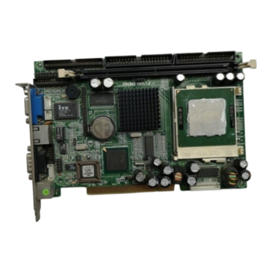
Page 7: Chapter 1 Introducing Thefb2642 System Board
The FB2642 is a Socket 370 all–in-one CPU card. This user’s manual provides information on the physical features, installation, and BIOS setup of the FB2642. Built to unleash the total potential of the Pentium Processor, the FB2642 is a single boards computer capable of handling today’s demanding requirements. Able to support up to1.3 MHz /Pentium-III/Tualatin/Celeron/Coppermine CPUs, this unit... -
Page 8: Layout
FabIATech Corporation Layout DIMM1 LED1... -
Page 9: Specifications
FabIATech Corporation Specifications Supports 600Mhz~1.300 GHz PIII/Tualatin/Celeron/Coppermine CPU. (Socket 370 with 0.18 and 0.13 micron technology) Compact size slot card with PICMG PCI expansion bus. Intel chipset 815E, ICH2 and 128KB or above L2 cache inside the CPUs. Supports one 168-pin DIMM socket (PC-100/133 SDRAM), 512MB maximum. -
Page 10: Packing List
Verify the accessories in the package according to the packing list and see if there is anything missing or incorrect package is included. • If the cable(s) you use to install the FB2642 is not supplied from us, please make sure the specification of the cable(s) is compatible with the FB2642 system board. -
Page 11: Chapter 2 Hardware Installation
FabIATech Corporation Chapter 2 Hardware Installation To set up a FB2642 system board, complete the description Chapter 2 and Chapter 3. This chapter introduces the system board connectors, jumper settings and then guides you to apply them for field application. -
Page 12: Hardware Features
FabIATech Corporation Hardware Features The following lists the connectors and jumpers to install the FB2642. Item Description 9-pin power connector CN2, CN3 Keyboard and Mouse connector 10-pin RS-232 port 2 connector RJ45-Lan connector 26-pin 2.0mm parallel port connector 34-pin 2.54mm floppy connector 40-pin 2.54mm IDE 1 hard disk connector... -
Page 13: Sw1 (3,4): Selecting Cpu Base Clock And Pci Clock
FabIATech Corporation SW1 (3,4): Selecting CPU Base Clock and PCI Clock DIMM1 LED1 The following lists the switch settings of CPU Base Clock and PCI clock. SW1-3 SW1-4 CPU Base Clock PCI Clock Remark 133 MHz 33 MHz Tualatlin Reserved... -
Page 14: J1 & J5: Cpu Fan Connector & System Fan Connector
FabIATech Corporation J1 & J5: CPU Fan Connector & System Fan Connector For CPU & system cooling fan DIMM1 J1, J5 LED1 J1&J5 Description Ground +12V Speed-In J2: USB Connector J2 is a 10-pin connector. Use included adapter cable (Optional) for transfering to standard double port USB connector. -
Page 15: J13: Reset Header
J13: Reset Header J13 is a 2-pin header for connecting to system reset bottom. Short-circuit these 2 pins to hardware reset FB2642 as well as restart system. It is similar to power off the system and then power it on again. -
Page 16: Cn2, Cn3: Keyboard/Mouse Connector
FabIATech Corporation CN2, CN3: Keyboard/Mouse Connector CN2 is a standard PS/2 type keyboard connector, so any PS/2 type keyboard can plug into CN2 directly without extra adapter cable. CN3 provides PS/2 mouse interface, use the included mouse adapter cable to connect between CN3 and standard PS/2 mouse. -
Page 17: Cn8, Cn9: Ide Hard Disk Connector
FabIATech Corporation CN8, CN9: IDE hard Disk Connector CN 8 is 40-pin 2.54mm IDE hard disk connector. CN9 is 44-pin 2.0mm IDC connectors. The included hard disk is able to attach up to four hard disk drives. CN8 – Hard disk connector... -
Page 18: Db1 & Cn4: Rs232 Serial Ports 1,2 Connectors And Jumpers
FabIATech Corporation DB1 & CN4: RS232 Serial Ports 1,2 Connectors and Jumpers The DB1 connector on bracket is 9-pin D-type male connector the serial port 2 adapter cables are used to transfer 10-pin IDC connector into standard DB9 connectors. DIMM1... - Page 19 FabIATech Corporation Signal RS422 RS485 -DCD2 -DSR2 RXD2 485- -RTS2 TXD2 485+ -CTS2 -DTR2 -RI2 GROUND CASE GROUND J12: 5-pin Infrared Header J12 provides infrared signals of serial port 2. The infrared signal is used to interface with Infrared modules.
-
Page 20: Cn6: 26-Pin Parallel Port Connector
FabIATech Corporation CN6: 26-pin Parallel Port Connector The included printer interface cable is used to transfer 26-pin connector into standard DB25 connector. DIMM1 LED1 CN6 DB-25 Signal CN6 DB-25 Signal -STROBE -AUTO FORM FEED DATA 0 -ERROR DATA 1 -INITIALIZE... -
Page 21: Cn7: Floppy Connector
FabIATech Corporation CN7: Floppy Connector The included floppy drive interface cable is used standard 34-pin connector. The following table shows signal connections 34-pin connectors. CN7 –Floppy connector DIMM1 LED1 34-pin Signal 34-pin Signal Drive Enable A Ground -Index -Write Enable... -
Page 22: J7: Temperature Sensor Header
FabIATech Corporation J7: Temperature Sensor Header DIMM1 LED1 Resistive Temperature Sensor Input Header JP1: CMOS Data Clear Jumper You can use JP1 to clear CMOS data. The CMOS store information like system date, time, boot up device, password, IRQ… that are set up with the BIOS. To clear the CMOS, set JP1 to 2-3 and then return to 1-2. -
Page 23: J6: Ttl I/O Connector
Bit 4 of 191h Input Line 1 Bit 5 of 191h Ground CN1: Power Connector (9-pin 2.54mm JST) CN1 is the power connector for FB2642 is used with stand-alone applications. DIMM1 LED1 Note: This power connector is ideal for standalone applications. -
Page 24: J8: External Tx-Led With Lan Led Header
Pin2 DB2: CRT connector The FB2642 supports a CRT colored monitor. It can be connected to create a compact video solution for the industrial environment. The VGA control in the 815E chipset and supports AGP, the VGA memory is UMA memory with 4MB caching buffer allows a maximum CRT resolution of 1280X1024 with 24bpp colors. -
Page 25: Chapter 3 Bios Setup
FabIATech Corporation Chapter 3 BIOS Setup This chapter describes the BIOS setup. Overview BIOS are a program located on a Flash memory chip on a circuit board. It is used to initialize and set up the I/O peripherals and interface cards of the system, which includes time, date, hard disk drive, the ISA bus and connected devices such as the video display, diskette drive, and the keyboard. -
Page 26: Bios Functions
FabIATech Corporation BIOS Functions On the menu, you can perform the following functions 1. Standard CMOS Setup 2. Advanced CMOS Setup 3. Advanced Chipset Setup 4. Power Management Setup 5. PCI/ Plug and Play Setup 6. Peripheral Setup 7. Hardware Monitor Setup 8. -
Page 27: Keyboard Convention
FabIATech Corporation Keyboard Convention On the BIOS, the following keys can be used to operate and manage the menu: Item Function To exit the current menu or message Page Up/Page Down To select a parameter To display the help menu if you do not know the... -
Page 28: Standard Cmos Setup
FabIATech Corporation STANDARD CMOS SETUP This section describes basic system hardware configuration, system clock setup and error handling. If the CPU board is already installed in a working system, you will not need to select this option anymore. Date & Time Setup Highlight the <Date>... - Page 29 FabIATech Corporation the master and slave jumpers, please refer to the hard disk’s installation descriptions and the hard disk jumper settings. You can select <AUTO> under the <TYPE> and <MODE> fields. This will enable auto detection of your IDE drives during boot up. This will allow you to change your hard drives (with the power off) and then power on without having to reconfigure your hard drive type.
-
Page 30: Advanced Cmos Setup
FabIATech Corporation ADVANCED CMOS SETUP This section describes the configuration entries that allow you to improve your system performance, or let you set up some system features according to your preference. Some entries here are required by the CPU board’s design to remain in their default settings. - Page 31 FabIATech Corporation –3 Boot Device These fields determine where the system attempts to look for the boot drive priority for an operating system. The default procedure is to check the hard disk, and then the floppy drive, and last the CDROM.
- Page 32 FabIATech Corporation Available options: On, Off Default setting: On Floppy Drive Swap The field reverses the drive letter assignments of your floppy disk drives in the Swap A, B setting, otherwise leave on the default setting of Disabled (No Swap). This works separately from the BIOS Features floppy disk swap feature.
- Page 33 FabIATech Corporation Default setting: Absent Password Check This field enables password checking every time the computer is powered on or every time the BIOS Setup is executed. If Always is chosen, a user password prompt appears every time and the BIOS Setup Program executes and the computer is turned on. If Setup is chosen, the password prompt appears if the BIOS executed.
- Page 34 FabIATech Corporation C000, 32k Shadow - E800, 32k shadow These fields control the location of the contents of the 32KB of ROM beginning at the specified memory location. If no adapter ROM is using the named ROM area, this area is made available to the local bus. The settings are: 1.
-
Page 35: Advanced Chipset Setup
FabIATech Corporation ADVANCED CHIPSET SETUP This section describes the configuration of the board’s chipset features. SDRAM Timing by SPD SPD represents Serial Presence Detect. It is an 8-bit, 2048 bits EEPROM, built on the SDRAM for 100 MHz frequencies. If the installed SDRAM supports SPD function, select SPD. - Page 36 FabIATech Corporation CAS# Latency (SCLKs) This field specifies the latency for the Synchronous DRAM system memory signals. Available Options: 3, 2 Default setting: 3 RAS# to CAS# delay (SCLKs) This field specifies the length of the delay inserted between RAS and CAS signals of the Synchronous DRAM system access cycle when SDRAM is installed.
- Page 37 FabIATech Corporation Default setting: 3 USB Function Select Enabled if a USB device is installed to the system. If Disabled are selected, the system will not be able to use a USB device. Available Options: Disabled, Enabled Default setting: Enabled USB Device Legacy Support Select All Device if a USB device is installed to the system.
-
Page 38: Power Management
FabIATech Corporation POWER MANAGEMENT Power Management /APM Select Enabled to activate the chipset Power Management and APM (Advanced Power Management) features. Available Options: Disabled, Enabled Default setting: Enabled Video Power Down Mode This field specifies the power conserving state that video subsystem enters after the specified period of display inactivity has expired. - Page 39 FabIATech Corporation Standby Time Out (Minute) This field specifies the length of a period of system inactivity (like hard disk or video) while in full power on state. When this length of time expires, the system enters Standby power state.
-
Page 40: Pci/Plug And Play
FabIATech Corporation PCI/PLUG AND PLAY Plug and Plug Aware O/S Set to Yes to inform BIOS that the operating system can handle Plug and Play (PnP) devices. Available Options: Yes, No Default setting: No PCI Latency Timer This field specifies the latency timings (in PCI clock) PCI devices installed in the PCI expansion bus. - Page 41 FabIATech Corporation PCI VGA Palette Snoop When Enabled is selected, multiple VGA devices operating on different buses can handle data from the CPU on each set of palette registers on every video device. Bit 5 of the command register in the PCI device configuration space is the VGA Palette Snoop bit.
- Page 42 FabIATech Corporation Default setting: PnP IRQ 3 –15 When I/O resources are controlled manually, you can assign each system interrupt as one of the following types, based on the type of device using the interrupt: ISA/EISA devices comply with the original PC AT bus specification, requiring a specific interrupt (Such as IRQ5 for COM1).
-
Page 43: Peripheral Setup
FabIATech Corporation PERIPHERAL SETUP This section describes the function of peripheral features. OnBoard FDC This field enables the floppy drive controller on the FB2642. Available Options: Disabled, Enabled and Auto Default setting: Auto OnBoard Serial Port 1 These fields select the I/O port address for each Serial port. Refer to Table 2-2. - Page 44 FabIATech Corporation OnBoard Parallel Port This field selects the I/O port address for parallel port. Available Options: Auto, Disabled, 378, 278, and 3BCH Default setting: Auto Parallel Port Mode This field specifies the parallel port mode. ECP and EPP are both bi-directional data transfer schemes that adhere to the IEEE P1284 specifications.
- Page 45 FabIATech Corporation On-Chip IDE This field specifies the IDE channel that can be applied when using CN3 IDE hard disk connector. Available Options: Disabled, Primary, and Secondary, Both Default setting: Both...
-
Page 46: Hardware Monitor Setup
FabIATech Corporation Hardware Monitor Setup On the Hardware Monitor Setup screen, you can set up or monitor the system temperature, CPU voltage, and CPU fan speed… System Hardware Monitor In this field, you can monitor or detect the followings items. These items are view-only and cannot be changed. -
Page 47: Password Setup
FabIATech Corporation Password Setup There are two security passwords: Supervisor and User. Supervisor is a privileged person that can change the User password from the BIOS. According to the default setting, both access passwords are not set up and are only valid after you set the password from the BIOS. - Page 48 FabIATech Corporation...
-
Page 49: Chapter 4 Driver And Utility
FabIATech Corporation Chapter 4 Driver and Utility The enclosed diskette includes FB2642 VGA driver and LAN driver. VGA Driver for WIN98/WIN95 Step 1: To install the VGA driver, insert the CD ROM into the CD ROM device, and enter DRIVER>VGA>I815e>WIN98. If your system is not equipped with a CD ROM device, copy the VGA driver from the CD ROM to a 1.44”... -
Page 50: Bios Flash Utility
FabIATech Corporation BIOS Flash Utility In the <UTILITY> directory, there is the FLASH835.EXE file. Step 1: Use the FLASH835.EXE program to update the BIOS setting. Step 2: And then refer to the chapter “BIOS Setup”, as the steps to modify BIOS. -
Page 51: Watchdog Timer
This section describes how to use the Watchdog Timer, including disabled, enabled, and trigger functions. The FB2642 is equipped with a programmable time-out period watchdog timer. You can use your own program to enable the watchdog timer. Once you have enabled the watchdog timer, the program should trigger the I/O every time before the timer times out. -
Page 52: Watchdog Timer Setting
FabIATech Corporation Watchdog Timer Setting The watchdog timer is a circuit that may be used from your program software to detect system crashes or hang-ups. The watchdog timer is automatically disabled after reset. Once you have enabled the watchdog timer, your program must trigger the watchdog timer every time before it times out. -
Page 53: Watchdog Timer Enable & Trigger
FabIATech Corporation Watchdog Timer Enable & Trigger After you enable the watchdog timer, your program must write the same factor as enabling to the watchdog register at least once every time-out period to its previous setting. You can change the time-out period by writing another timer factor to the watchdog register at any time, and you must trigger the watchdog before the new time-out period in the next trigger. -
Page 54: Watchdog Timer Disabled
FabIATech Corporation Watchdog Timer Disabled To disable the watchdog timer, simply write DisWD( ) function. #include “stdio.H” #include “WDLIB.H” main( ) InitWD(equWdUnitS); printf (“Disable Watch Dog”); //Disable watch dog DisWD( ); Programming RS-485 The majority communicative operation of the RS-485 is in the same of the RS-232. - Page 55 Disable TXC (transmitter control), the bit 0 of the address of offset+4 just sets “0”. NOTE: Control the FB2642 CPU card’s DTR signal to the RS-485’s TXC communication. Send out one character (Transmit) Step 1: Enable TXC signal, and the bit 0 of the address of offset+4 just sets “1”.
- Page 56 FabIATech Corporation Step 4: Disabled TXC signal, and the bit 0 of the address of offset+4 sets “0” Receive data The RS-485’s operation of receiving data is in the same of the RS-232’s. Basic Language Example a. Initial 86C450 UART OPEN “COM1:9600,m,8,1”AS #1 LEN=1...
- Page 57 REM Read one character from COM1: buffer INPSTR$=INPUT$(1,#1) RETURN NOTE: The example of the above program is based on COM1 (I/O Address 3F8h). The RS-422/RS-485 of the FB2642 uses COM2. If you want to program it, please refer to the BIOS Setup for COM2 address setup.
- Page 58 FabIATech Corporation...
-
Page 59: Chapter 5 Technical Reference
FabIATech Corporation Chapter 5 Technical Reference This section outlines the errors that may occur when you operate the system, and also gives you the suggestions on solving the problems. Topic include: Trouble Shooting for Error Messages Technical Reference Trouble Shooting for Error Messages The following information informs the error messages and troubleshooting. - Page 60 FabIATech Corporation CMOS CHECKSUM ERROR This error informs that the CMOS has corrupted. When the battery runs weak, this situation might happen. Please check the battery and change a new one when necessary. DISPLAY SWITCH IS SET INCORRECTLY Display switch on the motherboard can be set to either monochrome or color. This indicates the switch is set to a different setting than indicated in BIOS Setup.
- Page 61 FabIATech Corporation KEYBOARD ERROR OR NO KEYBOARD PRESENT When this situation happens, please check keyboard attachment and no keys being pressed during the boot. If you are purposely configuring the system without a keyboard, set the error halt condition in BIOS Setup to HALT ON ALL, BUT KEYBOARD.
-
Page 62: Technical Reference
Technical Reference Real-Time Clock and Non-Volatile RAM The FB2642 contains a real-time clock compartment that maintains the date and time in addition to storing configuration information about the computer system. It contains 14 bytes of clock and control registers and 114 bytes of general purpose RAM. - Page 63 FabIATech Corporation Address Description Low expansion memory byte High expansion memory byte 19-2D Reserved 2E-2F 2-byte CMOS checksum Low actual expansion memory byte High actual expansion memory byte Date century byte Information flags (set during power on) 34-7F Reserved for system BIOS...
-
Page 64: Cmos Ram Map
FabIATech Corporation CMOS RAM Map Register Description 00h -10h Standard AT-compatible RTC and Status and Status Register data definitions 11h – 13h Varies Equipment Bits Number of Floppy Drives 1 Drive 2 Drives Bits Monitor Type Not CGA or MDA 01 40x25 CGA... -
Page 65: I/O Port Address Map
FabIATech Corporation I/O Port Address Map Each peripheral device in the system is assigned a set of I/O port addresses, which also becomes the identity of the device. There is a total of 1K-port address space available. The following table lists the I/O port addresses used on the Industrial CPU Card. -
Page 66: Interrupt Request Lines (Irq)
FabIATech Corporation Interrupt Request Lines (IRQ) There are a total of 15 IRQ lines available on the Industrial CPU Card. Peripheral devices use interrupt request lines to notify CPU for the service required. The following table shows the IRQ used by the devices on the Industrial CPU Card. -
Page 67: Dma Channel Map
FabIATech Corporation DMA Channel Map The equivalent of two 8237A DMA controllers are implemented in the FB2650 board. Each controller is a four-channel DMA device that will generate the memory addresses and control signals necessary to transfer information directly between a peripheral device and memory. -
Page 68: Serial Ports
FabIATech Corporation Serial Ports The ACEs (Asynchronous Communication Elements ACE1 to ACE2) are used to convert parallel data to a serial format on the transmit side and convert serial data to parallel on the receiver side. The serial format, in order of transmission and reception, is a start bit, followed by five to eight data bits, a parity bit (if programmed) and one, one and half (five-bit format only) or two stop bits. - Page 69 FabIATech Corporation Bit 2: Enable Receiver Line Status Interrupt (ELSI) Bit 3: Enable MODEM Status Interrupt (EDSSI) Bit 4: Must be 0 Bit 5: Must be 0 Bit 6: Must be 0 Bit 7: Must be 0 Interrupt Identification Register (IIR) Bit 0: “0”...
- Page 70 FabIATech Corporation Bit 6: Set Break Bit 7: Divisor Latch Access Bit (DLAB) MODEM Control Register (MCR) Bit 0: Data Terminal Ready (DTR) Bit 1: Request to Send (RTS) Bit 2: Out 1 (OUT 1) Bit 3: Out 2 (OUT 2)
- Page 71 FabIATech Corporation Bit 5: Data Set Ready (DSR) Bit 6: Ring Indicator (RI) Bit 7: Received Line Signal Detect (RSLD) Divisor Latch (LS, MS) Bit 0: Bit 0 Bit 8 Bit 1: Bit 1 Bit 9 Bit 2: Bit 2...
-
Page 72: Parallel Ports
FabIATech Corporation Parallel Ports Register Address Port Address Read/Write Register Base + 0 Write Output data Base + 0 Read Input data Base + 1 Read Printer status buffer Base + 2 Write Printer control latch Printer Interface Logic The parallel portion of the SMC37C669 makes the attachment of various devices that accept eight bits of parallel data at standard TTL level. - Page 73 FabIATech Corporation Bit 7: This signal may become active during data entry, when the printer is off-line during printing, or when the print head is changing position or in an error state. When Bit 7 is active, the printer is busy and cannot accept data.
- Page 74 FabIATech Corporation Bit 5: Direction control bit. When logic 1, the output buffers in the parallel port are disabled allowing data driven from external sources to be read; when logic 0, they work as a printer port. This bit is write-only.
-
Page 75: Appendix
FabIATech Corporation Appendix Dimension 184.9 Unit: mm... -
Page 76: Special Features
J3: Feature Connector (J3: 44-pin 2.0mm IDC) J3 is a multi-function connector which supports signals for AC97 audio, Panel Link, and Intel LAN solution. FabiaTech provides FB4641 (Audio and USB Adapter Board for FB2642, Optional) for Audio functions. J3 – Feature connector The following table lists the pin description of J3.
Need help?
Do you have a question about the FB2642 and is the answer not in the manual?
Questions and answers