
Subscribe to Our Youtube Channel
Related Manuals for NXP Semiconductors LPCXpresso54102


Summary of Contents for NXP Semiconductors LPCXpresso54102
- Page 1 UM10855 LPCXpresso54102 Rev. 1.0 — 4th November 2014 User manual Document information Info Content Keywords LPCXpresso54102, LPC54100 Abstract LPCXpresso54102 User Manual...
- Page 2 UM10855 NXP Semiconductors LPCXpresso board for LPC54100 family of MCUs Revision history Date Description <20141105> OM13077 User Manual release Contact information For more information, please visit: http://www.nxp.com For sales office addresses, please send an email to: salesaddresses@nxp.com UM10855_OM1377.docm All information provided in this document is subject to legal disclaimers.
-
Page 3: Introduction
NXP's Cortex®-M family of MCUs. They can be used with a wide range of development tools, including the NXP’s LPCXpresso IDE. The LPCXpresso54102 board has been developed by NXP to enable evaluation of and prototyping with the LPC54100 family of MCUs, and is based on the LPC54102J512BD64 version of the MCU. -
Page 4: Board Layout And Settings
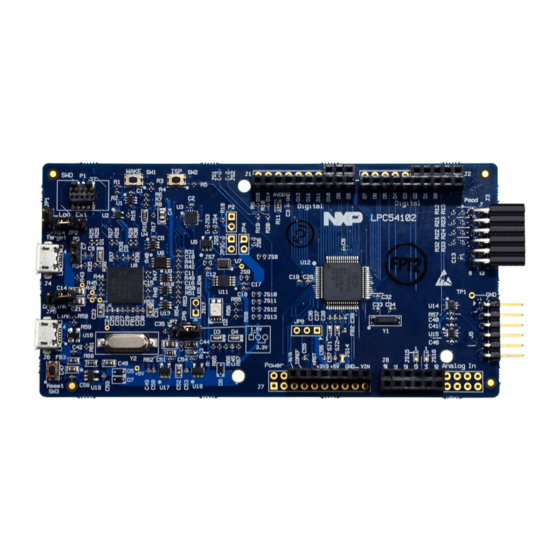
2.1 Board layout and settings This section provides a quick reference guide to the main board components, configurable items, visual indicators and expansion connectors. The layout of the components on the LPCXpresso54102 board is shown in Figure 1 below: Figure 1 Board Layout The function of each identified component is listed in Table 1. - Page 5 UM10855 NXP Semiconductors LPCXpresso board for LPC54100 family of MCUs Designator Description Reference section LPC54102 Target Power input. Connect this micro USB B- type connector to a +5V power source when it is desired to power only the LPC54102 Target, and leave the on-board Link2 debug probe unpowered.
-
Page 6: Getting Started
LPC54102 Target LQFP64 MCU 3. Getting Started By default, the LPCXpresso54102 is configured to use the on-board debug probe (Link2) to debug the on-board target (LPC54102), using the CMSIS-DAP debug protocol pre- programmed into the Link2 Flash memory. The LPCXpresso IDE (available for free download at http://www.lpcware.com/lpcxpresso/home) or development tools that... -
Page 7: Lpc54102 Serial Ports
1) Download and install the LPCXpresso Link2 USB driver package installer from http://www.lpcware.com/content/nxpfile/lpcxpresso-link2-usb-driver-package (only required if using Windows). 2) When the installer has completed, connect the LPCXpresso54102 board to the USB port of your host computer, connecting a micro USB cable to connector J6 (“Link”). - Page 8 UM10855 NXP Semiconductors LPCXpresso board for LPC54100 family of MCUs Figure 2 – FTDI (J5) LPC54102 serial port Table 2 – J5 FTDI interface LPC54102 Signal FTDI Pin # Direction Signal No connect Board +5V UART0_RXD From host UART0_TXD To host No connect UM10855_OM1377.docm...
-
Page 9: Board Power Connections & Measurement
LPCXpresso board for LPC54100 family of MCUs 5. Board power connections & measurement The LPCXpresso54102 board requires +5V input to power the on-board voltage regulators which in turn power the Link2 debug probe and other +3.3V circuits, the LPC54102 target and other +1.8V circuits, and the Arduino +5V and +3.3V power rails. -
Page 10: Lpc54102 Vsense Resistor Current Measurement
UM10855 NXP Semiconductors LPCXpresso board for LPC54100 family of MCUs 5.1.1 LPC54102 Vsense resistor current measurement The voltage across a series 8.2Ω resistor with the target LPC54102 VDD can be manually measured at P2 on the PCB. The voltmeter positive probe is applied to P2 pin 1 (square pad) and negative probe to P2 pin 2, see Figure 4. -
Page 11: Lpc54102 Vdd Current Measurement
6. Debug Configurations The LPCXpresso54102 LQFP board has a built-in debug probe using the Link LPC43xx MCU. The LPC54102 target MCU can be debugged by the on-board Link debugging probe, or from an external debug probe installed at P1. On-board jumpers JP1 and JP2 must be correctly positioned for each mode. -
Page 12: Debug On-Board Lpc54102 Target Using External Debug Probe
UM10855 NXP Semiconductors LPCXpresso board for LPC54100 family of MCUs Figure 7 – Debug local LPC54102 target from on-board debug probe 6.1.2 Debug on-board LPC54102 target using external debug probe To use an external debug probe, connect the probe to the SWD (P1) connector, power... -
Page 13: Using On-Board Link2 To Debug An Off-Board Target Lpc Mcu
Figure 9 - Link LPC43xx MCU DFU mode 6.2 Using on-board Link2 to debug an off-board target LPC MCU The LPCXpresso54102 board’s Link2 debug probe may be used to debug an off-board target MCU. The on-board Link debug probe is capable of debugging target MCU’s with a VDDIO range of 1.6V to 3.6V. -
Page 14: Expansion Connectors
8. Expansion connectors The LPCXpresso54102 board includes four expansion connectors plus a PMod™ compatible connector (J3). The expansion connectors (J1, J2, J7 and J8) incorporate an Arduino Uno revision 3 footprint in their inner rows. Not all connector locations are populated on the expansion connectors since the LPC54102 does not have enough I/O UM10855_OM1377.docm... -
Page 15: Buttons
LPC54102 signals not used by the Arduino Uno rev3 compatible interface. 9. Buttons The LPCXpresso54102 board has 3 push buttons available to control the operation of the LPC54102 (target) MCU. Their functions are as described below. 9.1 Reset This button is used to reset the LPC54102. -
Page 16: Legal Information
Semiconductors products in order to avoid a default of the applications and In no event shall NXP Semiconductors be liable for any indirect, incidental, the products or of the application or use by customer’s third party punitive, special or consequential damages (including - without limitation - customer(s). -
Page 17: List Of Figures
............... 12 Figure 9 - Link LPC43xx MCU DFU mode ......13 Figure 10 - Link debug probe debugging off-board target . 13 Figure 11 – LPCXpresso54102 LQFP board LED Indicators ................ 14 UM10855_OM1377.docm All information provided in this document is subject to legal disclaimers. -
Page 18: List Of Tables
UM10855 NXP Semiconductors LPCXpresso board for LPC54100 family of MCUs 12. List of tables Table 1 - Board interface components ........ 4 Table 2 – J5 FTDI interface ..........8 Table 3 - Board LED indicators ......... 14 Table 4 Expansion Connectors ......... 15 UM10855_OM1377.docm... -
Page 19: Table Of Contents
Board layout and settings ........4 Getting Started ............ 6 LPC54102 Serial ports ........7 J5 FTDI header ..........7 Board power connections & measurement..9 LPCXpresso54102 current measurement ..9 5.1.1 LPC54102 Vsense resistor current measurement ................. 10 5.1.2 LPC54102 external sense resistor for VDD current measurement ........ - Page 20 Mouser Electronics Authorized Distributor Click to View Pricing, Inventory, Delivery & Lifecycle Information: OM13077 OM13077UL...
Need help?
Do you have a question about the LPCXpresso54102 and is the answer not in the manual?
Questions and answers