
Related Manuals for NXP Semiconductors LPC55 Series


Summary of Contents for NXP Semiconductors LPC55 Series
- Page 1 LPCXpresso55S9UM11158 UM11158 LPCXpresso55S69 Development Board Rev. 1.2 — 25 April 2019 User manual Document information Info Content Keywords LPC55S69, LPC55xx, LPCXpresso55S69, LPC55S69-EVK Abstract LPCXpresso55S69 user manual...
- Page 2 UM11158 NXP Semiconductors LPCXpresso55S69 Development Board Revision history Date Description 20180816 Initial internal release 20181015 Added official document number. Section 4 updated/corrected. 20190308 Added references in jumper/connector Indicators/buttons/connector table. Added notes about 3.3V only operation of Revision A/A1 boards. Added new figures for expansion connectors.
-
Page 3: Introduction
UM11158 NXP Semiconductors LPCXpresso55S69 Development Board 1. Introduction The LPCXpresso™ family of boards provides a powerful and flexible development system for NXP's LPC Cortex®-M family of MCUs. They can be used with a wide range of development tools, including NXP’s MCUXpresso IDE. The LPCXpresso55S69 board (order code LPC55S69-EVK) is the evaluation and development platform for the LPC556x family of MCUs. - Page 4 UM11158 NXP Semiconductors LPCXpresso55S69 Development Board • RGB user LED • Reset, ISP, User/Wakeup and user buttons • Multiple Expansion options, including Arduino UNO, Mikroe Click and PMod • Micro SD card slot • NXP MMA8652FCR1 accelerometer • Stereo audio codec with line in/out •...
-
Page 5: Board Layout And Settings
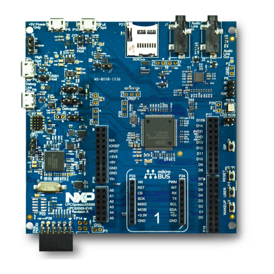
UM11158 NXP Semiconductors LPCXpresso55S69 Development Board 2. Board layout and Settings Figure 2 shows the layout of the board (top side), indicating location of the connectors and buttons, while Figure 3 shows locations of jumpers and headers. Table 1 provides a description of connectors, jumpers, LEDs and buttons. - Page 6 UM11158 NXP Semiconductors LPCXpresso55S69 Development Board Fig 3. LPCXpresso55S69 jumpers and headers Table 1. Indicators, buttons, connectors and LEDs Circuit Description Default Reference reference Target power indicator LED Link2 boot LED Section 4.1 RGB User LED Section 7.4 Audio codec line input jack Section 7.1...
- Page 7 UM11158 NXP Semiconductors LPCXpresso55S69 Development Board Table 1. Indicators, buttons, connectors and LEDs Circuit Description Default Reference reference Target processor selection for the on-board Debug Probe. Not installed Section 4. Jumper open (default) the LPC55S69 Target SWD interface enabled. Normal operating mode where the Target SWD is connected to either the on-board Link2 Debug Probe or an external Debug Probe.
- Page 8 UM11158 NXP Semiconductors LPCXpresso55S69 Development Board Table 1. Indicators, buttons, connectors and LEDs Circuit Description Default Reference reference Serial port header Section 6.2 0.1” header providing convenient access to Flexcom 0 USART (the USART used for ISP boot). When using this port install jumper P1 to disable the Link2 connection to this port.
-
Page 9: Getting Started
UM11158 NXP Semiconductors LPCXpresso55S69 Development Board Table 1. Indicators, buttons, connectors and LEDs Circuit Description Default Reference reference ISP/User button Section 7.5.1 When pressed, this button connect sport pin P0_5 to ground. Hold this button down while pressing and releasing Reset (S4) to force the LPC55S69 into ISP mode. -
Page 10: Starting A Debug Session Using The On-Board (Link2) Debug Probe
UM11158 NXP Semiconductors LPCXpresso55S69 Development Board development tools that support the CMSIS-DAP protocol can be used in the default configuration. Check with your toolchain vendor for availability of specific device support packs for the LPC55S69 series devices. Note that when using the MCUXpresso IDE, the on-board Link2 can also be booted in DFU mode by installing a jumper on J4;... -
Page 11: Installation Steps To Use Keil And Iar Tools With On-Board Debug Probe
UM11158 NXP Semiconductors LPCXpresso55S69 Development Board The Link2 Debug Probe on the board will have been programmed with CMSIS-DSP firmware during manufacture, but can also be updated with J-link OB for LPC-Link2. To start the board with this firmware running, ensure J4 is not installed as power is connected, so the Link2 Debug Probe boots from internal flash. -
Page 12: On-Board (Link2) Debug Probe
UM11158 NXP Semiconductors LPCXpresso55S69 Development Board 4. On-board (Link2) Debug probe This section describes the features provided by the on-board Link2 Debug Probe, including how to use this to debug an exernal target. The Link2 Debug Probe is implemented using an LPC432x MCU (circuit reference U2), which provides a high speed USB port interface to the host computer that runs the development tools. -
Page 13: Link2 Boot Led
UM11158 NXP Semiconductors LPCXpresso55S69 Development Board 4.1 Link2 boot LED LED DS2 is the Link2 MCU BOOT0_LED indicator. This LED reflects the state of Link2 MCU pin P1_1. When the boot process fails, DS2 will toggle at a 1 Hz rate for 60 seconds. -
Page 14: Board Power
UM11158 NXP Semiconductors LPCXpresso55S69 Development Board 5. Board Power The LPCXpresso55S69 board requires +5V input to power the on-board voltage low dropout linear regulators, of which there are 3, all available from Torex Semiconductor. The Link2 Debug probe has a 2.5V regulator (U10) which draws power from USB connector P6 (“Debug Link”) only. -
Page 15: Usart Header
UM11158 NXP Semiconductors LPCXpresso55S69 Development Board The Board can only be configured to support one of these ports as a host at a time (this is a limitation of the board, not the LPC55S69). When either port is used as a host, power must be supplied to the board via the +5V power only micro B USB port. -
Page 16: Micro Sd Card Slot
UM11158 NXP Semiconductors LPCXpresso55S69 Development Board 7.2 Micro SD card slot The micro SD card (P21) included in the LPCXpresso55S69 board provides a 4-bit SDIO interface to support memory cards, plug-in WiFi modules, etc. Power enable to the socket is provided via transistor enabled by P1_0. -
Page 17: Isp (S1)
UM11158 NXP Semiconductors LPCXpresso55S69 Development Board 7.5.1 ISP (S1) P0_5 is pulled up to VDD via a 2.2 kohm resistor; pressing this button will pull P0_5 low. This port is read by the LPC55S69 boot code to determine if the MCU should enter In System Programming (ISP) mode. -
Page 18: Arduino And Lpcxpresso V3 Expansion Connectors
UM11158 NXP Semiconductors LPCXpresso55S69 Development Board can be installed and used to provide an external reset control input from the host, The connector footprint and connection can also be used to connect to external PMod peripherals that follow the PMod I2C, or SPI (Type 2 or 2A) standards. Refer to the PMod specifications from Digilent Inc. - Page 19 UM11158 NXP Semiconductors LPCXpresso55S69 Development Board Fig 4. P16 and P19 connector pinouts Fig 5. P17 and P18 connector pinouts UM11158 All information provided in this document is subject to legal disclaimers. © NXP B.V. 2019. All rights reserved. User manual Rev.
-
Page 20: Board Power
UM11158 NXP Semiconductors LPCXpresso55S69 Development Board SDIO port 1 of the LPC55S69 is routed to the expansion connector to provide access to this interface. Note that the power enable signal used for this SDIO interface is not one of the port pins that supports in SD1_POWER_EN function; this because all port pins that support this function are required for other features of the board. -
Page 21: Legal Information
Customers should provide appropriate design and operating safeguards to minimize the risks associated with their applications and products. NXP Semiconductors does not accept any liability related to any default, damage, costs or problem which is based on any weakness or default in the customer’s applications or products, or the application or use by customer’s third party customer(s). -
Page 22: Table Of Contents
UM11158 NXP Semiconductors LPCXpresso55S69 Development Board 11. Contents Introduction ......3 Board layout and Settings ....5 Getting started . - Page 23 UM11158 NXP Semiconductors LPCXpresso55S69 Development Board UM11158 All information provided in this document is subject to legal disclaimers. © NXP B.V. 2019. All rights reserved. User manual Rev. 1.2 — 25 April 2019 23 of 24...
- Page 24 UM11158 NXP Semiconductors LPCXpresso55S69 Development Board UM11158 All information provided in this document is subject to legal disclaimers. © NXP B.V. 2019. All rights reserved. User manual Rev. 1.2 — 25 April 2019 24 of 24...
Need help?
Do you have a question about the LPC55 Series and is the answer not in the manual?
Questions and answers