Table of Contents
Advertisement
Quick Links
November 2009
Downloaded from
Elcodis.com
electronic components distributor
Introduction
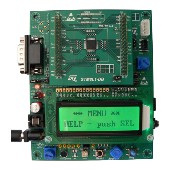
The STM8L101-EVAL is composed of two boards:
An STM8L1/L2 motherboard called MB709 which includes all peripherals which are
connected to the MCU on the daughterboard. The motherboard connects to the
daughterboard via two 36-pin connectors.
An STM8L1 daughterboard called MB710 which has an STM8L101 MCU.
The motherboard and daughterboard are a complete development platform for
STMicroelectronic's STM8L101 microcontroller with comparator, I2C, SPI, USART and
SWIM debugging support.
The full range of hardware features on the STM8L101-EVAL helps you to evaluate all
TM
peripherals (MicroSD card
applications.
Figure 1.
STM8L101-EVAL board
, USART, EEPROM, LCD, for example) and develop your own
Doc ID 15312 Rev 2
UM0629
User Manual
STM8L101-EVAL
evaluation board
1/26
www.st.com
Advertisement
Table of Contents

Related Manuals for ST STM8L101-EVAL


Summary of Contents for ST STM8L101-EVAL
- Page 1 The motherboard and daughterboard are a complete development platform for STMicroelectronic's STM8L101 microcontroller with comparator, I2C, SPI, USART and SWIM debugging support. The full range of hardware features on the STM8L101-EVAL helps you to evaluate all peripherals (MicroSD card , USART, EEPROM, LCD, for example) and develop your own applications.
-
Page 2: Table Of Contents
Contents UM0629 Contents Overview ..........4 Features . - Page 3 Contents Appendix A STM8L101-EVAL I/O assignment ......24 Revision history ......... . . 25...
-
Page 4: Overview
For more information and to download the latest version available, refer to STM8L101-EVAL demonstration firmware available on web: www.st.com/mcu. Order code To order the STM8L101K3 evaluation board, use the order code STM8L101-EVAL. 4/26 Doc ID 15312 Rev 2 Downloaded from Elcodis.com... -
Page 5: Hardware Layout And Configuration
UM0629 Overview Hardware layout and configuration The STM8L101-EVAL evaluation board is designed around the STM8L101K3T6 in an LQFP32 package. Figure 2 illustrates the connections between the daughterboard and the peripherals on the motherboard (LCD, I2C EEPROM, USART, audio and MicroSD card). - Page 6 Overview UM0629 Figure 3. STM8L1/L2 motherboard layout CN3, CN4 daughterboard connectors SWIM (ERNI cable alternative) SWIM Potentiometer USART Dot-matrix LCD Micro SD card™ Audio jack CN10 5V power MCU_VDD RESET Joystick adjustment 6/26 Doc ID 15312 Rev 2 Downloaded from Elcodis.com electronic components distributor...
- Page 7 UM0629 Overview Figure 4. STM8L1 daughterboard layout CN1, CN2 motherboard connector STM8L101 MCU in LQFP32 package soldered directly onto the board and footprint for socket (ref ENPLAS OTQ-32-0.8-02) is present on the board Doc ID 15312 Rev 2 7/26 Downloaded from Elcodis.com electronic components distributor...
-
Page 8: Stm8L1/L2 Motherboard
STM8L1/L2 motherboard UM0629 STM8L1/L2 motherboard This motherboard is designed to work with an STM8L1 daughterboard. Power supply The motherboard is designed to be powered by a 5 V DC power supply and to be protected from a wrong power plug-in event by PolyZen Inc. (auto rearmable fuse) U13. It is possible to configure the evaluation board to provide 5 V power to the daughterboard through the daughterboard connector. -
Page 9: Reset Source
UM0629 STM8L1/L2 motherboard Reset source The reset signal of the motherboard is low active. Reset sources include: Reset button B1. Debugging tools from connectors CN5, CN6. The reset pin PA1 of the STM8L101 is either connected to the reset button B1 or to GND by the setting of jumper JP1: Table 2. -
Page 10: I2C Eeprom
STM8L1/L2 motherboard UM0629 I2C EEPROM A 64 Kbit I2C EEPROM is connected to the I2C port of the STM8L101. Write protection can be enabled by the setting of jumper JP8. Table 4. I2C EEPROM related jumpers Jumper Description I2C EEPROM U6 is protected from write operation when JP8 is not fitted. Default setting: Fitted RS-232 One D-type 9-pin RS-232 connector CN8 is available on the motherboard. -
Page 11: Display And Input Devices
UM0629 STM8L1/L2 motherboard Display and input devices Display devices available are: 122x32 dot-matrix serial interface LCD (U2) 4 general purpose LED's (LD2,3,4,5) Input devices available are: 4-direction joystick selection key general purpose button (B2) Table 5. 122x32 dot matrix LCD U13 Pin on U2 Description Pin connection... -
Page 12: Microsd Connector Cn1
STM8L1/L2 motherboard UM0629 Figure 5. Voltage measurement using internal comparator Table 6. Potentiometer RV1 related jumpers Jumper Description Setting RV1 is connected to PD2 as one input of the internal comparator when JP2 1 2 3 is set as shown to the right: JP2 position is called Comp_PD2 on the silk-screen. -
Page 13: Daughterboard Extension Connectors Cn3 And Cn4
UM0629 STM8L1/L2 motherboard Table 7. MicroSD connector CN1 Pin number Description Pin number Description Reserved SCLK/PB5 CS/PB4 Vss/GND DI/PB6 DO/PB7 Reserved Not used 2.13 Daughterboard extension connectors CN3 and CN4 Two 36-pin male headers CN3 and CN4 can be used to connect the daughterboard to the motherboard. -
Page 14: Swim Connectors Cn5 And Cn6
STM8L1/L2 motherboard UM0629 Table 9. Daughterboard extension connector CN4 Pin number Description Pin number Description Reserved Reserved Reserved Reserved RESET# Reserved Reserved Reserved Reserved MCU_VDD Reserved Reserved Reserved Reserved Reserved Reserved Reserved Reserved 2.14 SWIM connectors CN5 and CN6 CN6 is a low cost 2.54 mm pitch connector to be used by customers who do not have the ERNI cable. -
Page 15: Rs-232 Connector Cn8
UM0629 STM8L1/L2 motherboard 2.15 RS-232 connector CN8 Figure 8. RS-232 connector CN8 viewed from front Table 11. RS-232 connector CN8 Pin number Description Pin number Description Connect to Pin 4 USART_RXD/PC2 Connect to Pin 8 USART_TXD/PC3 Connect to Pin 7 Connect to Pin 6 2.16 Audio jack CN9... -
Page 16: Stm8L1 Daughterboard
STM8L1 daughterboard UM0629 STM8L1 daughterboard Power The STM8L101 MCU is powered by MCU_VDD from the motherboard through an extension connector on the board. It is enabled by setting the jumper JP1 as described in Table Table 12. Power related jumper* Jumper Description Enables consumption measurement of VDD when the jumper is removed and replaced by... -
Page 17: Schematics
Schematics STM8L1/L2 motherboard Figure 10. STM8L1 motherboard schematic U_Audio U_MCU U_Peripherals Audio.SchDoc MCU.SchDoc Peripherals.SchDoc MIC_OUT MIC_OUT I2C_SLK I2C_SLK Audio_PWM Audio_PWM I2C_SDA I2C_SDA BEEP BEEP LED4 LED4 LED3 LED3 U_LCD_MicroSD LED2 LED2 LCD_MicroSD.SchDoc LED1 LED1 SPI_MISO SPI_MISO BiD_LED BiD_LED SPI_MOSI SPI_MOSI USART_RX USART_RX SPI_SCK... - Page 18 Figure 11. STM8L1 motherboard MCU MCU_VDD 20pF 20pF RESET# MCU_VDD VDDA RESET# Not Fitted RESET EX_PC5 EX_PC6 BEAD 100nF 10uF 100nF 100nF Not Fitted 10nF 11 12 VDDA 13 14 15 16 17 18 19 20 21 22 solder bridge PA1/NRST PA0/SWIM/BEEP/IR_TIM BEEP...
- Page 19 Figure 12. STM8L1 motherboard LCD and SD SDcard_detect +3V3 +3V3 9013 PJS008-2000 (SMS064FF or SMS128FF) MicroSD_CS MicroSD card +3V3 MCU_VDD +3V3 100nF 100nF +3V3 MCU_VDD do not fit do not fit 100nF SPI_SCK IOVL_1 IOVCC_1 do not fit SPI_MOSI IOVL_2 IOVCC_2 LCD_CS IOVL_3...
- Page 20 Figure 13. STM8L1 motherboard peripherals MCU_VDD VCCA VCCB MCU_VDD BiD_LED SN74LVC1T45DCKT MCU_VDD L-317EGW-SS +3V3 MCU_VDD LED1 VB334 (do not fit) Bi-color LED Green BNC connector User_Button LED2 Orange USER MCU_VDD LED3 100nF 100nF Blue MCU_VDD LED4 I2C_SLK Potentiometer I2C_SDA M24C64-RMN6 Potentiometer User Button LEDs...
- Page 21 Figure 14. STM8L1/L2 motherboard audio +3V3 Speaker- 470pF KDMG15008-03 Audio_PWM JP10 Audio 1.2K ST-613 Speaker+ Standby Uout1 33nF +3V3 Vin- Vout2 Vin+ 2.2uF Bypass 0(don't solder) 100uF TS4871IST 100nF BEEP 2.2uF Speaker MCU_VDD MCU_VDD 10uF KECG2740TBL 2.2K MIC_OUT MIC+ TS461CLT...
- Page 22 Figure 15. STM8L1 motherboard power ZEN056V130A24LS +3V3 LD1086D2M33 +3V3 CN10 MCU_VDD Vout 10uF 470uF 10uF 100nF DC-10B JP11 SMAJ5.0A-TR 100nF BNX002-01 VCC_ADJ LD1086D2M VCC_ADJ JP12 Ground Vout 100nF Header 2X2 10uF 3314J-201 STMicroelectronics Title: STM8L1/L2-MB Power MB709 Rev: A.1(PCB.SCH) Date: 9/23/2009 Number: Downloaded from Elcodis.com...
-
Page 23: Stm8L1-Db Daughterboard Schematic
STM8L1-DB daughterboard schematic Figure 16. Daughterboard schematic PA1/NRST PA0/SWIM/BEEP/IR_TIM QTH-030-01-L-D-A RESET# PA4/TIM2_BKIN PC4/USART_CK/CCO PA5/TIM3_BKIN PC3/USART_TX PA6/COMP_REF PC2/USART_RX MCU_VDD PC1/I2C_SCL PC0/I2C_SDA PD0/TIM3_CH2/COMP1_CH3 PD1/TIM3_TRIG/COMP1_CH4 100nF PD2/COMP2_CH3 PD3/COMP2_CH4 PB0/TIM2_CH1/COMP1_CH1 PB7/SPI_MISO PB1/TIM3_CH1/COMP1_CH2 PB6/SPI_MOSI PB2/ TIM2_CH2/COMP2_CH1 PB5/SPI_SCK PB3/TIM2_TRIG/COMP2_CH2 PB4/SPI_NSS STM8L101K3T QFP32 and OTQ-32-0.8-02 double footprint Left Right RESET#... - Page 24 STM8L101-EVAL I/O assignment UM0629 Appendix A STM8L101-EVAL I/O assignment Table 13. STM8L101-EVAL input and output assignment STM8L101 STM8L101-EVAL pin STM8L101 STM8L101-EVAL pin Pin name Pin name pin number assignment pin number assignment PA1 - NRESET RESET SD_card_CS Unused SPI_SCK Unused...
- Page 25 UM0629 Revision history Revision history Table 14. Document revision history Date Revision Changes 29-Jan-2009 Initial release. Removed STice and IrDA functionality. Modified , Section 2.5, 06-Nov-2009 Section 2.6 Table Table Table Table Table Figure Figure Figure 4 all schematics and Appendix Doc ID 15312 Rev 2 25/26...
- Page 26 No license, express or implied, by estoppel or otherwise, to any intellectual property rights is granted under this document. If any part of this document refers to any third party products or services it shall not be deemed a license grant by ST for the use of such third party products or services, or any intellectual property contained therein or considered as a warranty covering the use in any manner whatsoever of such third party products or services or any intellectual property contained therein.
Need help?
Do you have a question about the STM8L101-EVAL and is the answer not in the manual?
Questions and answers