Table of Contents
Advertisement
Quick Links
Advertisement
Table of Contents

Related Manuals for Measurement Computing CIO-DAC08/16


Summary of Contents for Measurement Computing CIO-DAC08/16
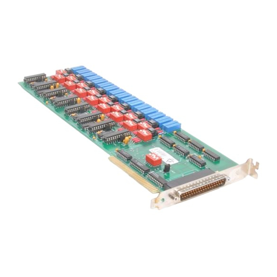
- Page 1 CIO-DAC08/16 CIO-DAC16/16 User’s Manual Revision 6 April, 2001...
- Page 2 Information furnished by Measurement Computing Corporation is believed to be accurate and reliable. However, no responsibility is assumed by Measurement Computing Corporation neither for its use; nor for any infringements of patents or other rights of third parties, which may result from its use. No license is granted by implication or otherwise under any patent or copyrights of Measurement Computing Corporation.
-
Page 3: Table Of Contents
Table of Contents 1.0 INTRODUCTION ..........2.0 SOFTWARE INSTALLATION . - Page 4 This page is blank.
-
Page 5: Introduction
1.0 INTRODUCTION The CIO-DAC16/16 is a 16-channel analog output board. The CIO-DAC08/16 is an 8-channel analog output board. The analog outputs are from AD660BNs with each output buffered by an OP-27. The analog outputs are controlled by writing a digital control word as two bytes to the DAC's control register. -
Page 6: Hardware Installation
The base address switch for the CIO-DAC16/16 is shown here, set to 300 hex. The CIO-DAC08/16 has one additional switch on the base address switch bank (A4 with a weight of 10 hex). Figure 3-1. Base Address Switches (Set to 300h) The address switches may be set for a base address in the range of 000-3E0 (3F0 for the DAC08) so it should not be hard to find a free address area. - Page 7 Table 3-1. PC I/O Addresses FUNCTION FUNCTION RANGE RANGE 000-00F 8237 DMA #1 2C0-2CF 020-021 8259 PIC #1 2D0-2DF 040-043 8253 TIMER 2E0-2E7 GPIB (AT) 060-063 8255 PPI (XT) 2E8-2EF SERIAL PORT 060-064 8742 CONTROLLER (AT) 2F8-2FF SERIAL PORT 070-071 CMOS RAM &...
-
Page 8: Analog Output Range Jumpers
3.2 ANALOG OUTPUT RANGE JUMPERS The analog output voltage range of each channel is set with a jumper. The jumpers are located on the board directly below the calibration potentiometers and are labeled J1 through J8 on the DAC08 and. J1 through J16 on the DAC16. Set the jumpers for an individual channel as shown in Figure 3-2. -
Page 9: Simultaneous Update Jumper
This jumper affects ONLY the power-up / reset condition of the DACs. It is here to insure that when the computer is turned on, or, if the computer is reset, process controls will come up in a known, safe state. Figure 3-3. -
Page 10: Installing The Boards In The Computer
Note: Use simultaneous update to maintain power-up state (see section on “Initial Zero State Jumper”). In this way, the CIO-DAC16/16 and DAC08/16 may be set to hold new values until all channels are loaded, then update all sixteen simultaneously. This can be a very useful feature for multi-axis motor control. -
Page 11: Signal Connection
3.7 SIGNAL CONNECTION The analog outputs of the CIO-DAC16/16 and the DAC08/16 are two-wire hook-ups; a signal, labeled D/A # OUT on the connector diagram after this section, and a Low Level Ground (LLGND). The low level ground is an analog ground and is the ground reference which should be used for all analog hook-ups. -
Page 12: Connector Diagram
The connector accepts female 37-pin, D-type connectors, such as those on the C37FF-2, a 2-foot cable with connectors. If frequent changes to signal connections or signal conditioning is required, please refer to the information on the CIO-TERMINAL, CIO-SPADE50 and CIO-MINI37 screw terminal boards in the Measurement Computing catalog. -
Page 13: Register Architecture
BASIC, C or PASCAL. 4.1 CONTROL & DATA REGISTERS The CIO-DAC16/16 has 32 analog output registers, the CIO-DAC08/16 has 16. There are two for each channel, one for the lower eight bits and one for the upper eight bits. -
Page 14: Output Transfer Functions
In summary form, the registers and functions are listed in Table 4-2. Each register has eight bits which may constitute a byte of data or eight individual bit functions. Table 4-2. Register Summary ADDRESS WRITE FUNCTION READ FUNCTION BASE + 0 D/A 0 Least Significant Byte Initiate simultaneous update. - Page 15 FSV / 65,536 * CODE = OutV CODE = OutV / FSV * 65,536 For Example: If the range is 0 to 5V CODE = 2/5 * 65,536 and you desire a 2V output. CODE = 26,214 The BIPOLAR transfer function for the DAC is: FSV/65,536 * CODE −...
-
Page 16: Specifications
5.0 SPECIFICATIONS Power Consumption +5V supply CIO-DAC16/16 1.8A typical, 2.25 max CIO-DAC08/16 1.3A typical, 1.7A max Analog Output Resolution 16 bits Number of channels CIO-DAC16/16 16 Voltage Output CIO-DAC08/16 8 Voltage Output D/A type AD660BN Voltage Ranges ±5V, ±10V, 0 to 5V, 0 to 10V, jumper... - Page 17 For your notes.
- Page 18 For your notes.
- Page 19 EC Declaration of Conformity We, Measurement Computing Corp., declare under sole responsibility that the product: CIO-DAC16/16 16 Channel analog output board CIO-DAC08/16 8 Channel analog output board Part Number Description to which this declaration relates, meets the essential requirements, is in conformity...
- Page 20 Measurement Computing Corporation 16 Commerce Boulevard, Middleboro, MA 02346 (508) 946-5100 Fax: (508) 946-9500 E-mail: info@measurementcomputing.com www. measurementcomputing.com Measurement Computing Corporation 10 Commerce Way Suite 1008 Norton, Massachusetts 02766 (508) 946-5100 Fax: (508) 946-9500 E-mail: info@mccdaq.com www.mccdaq.com RegMapPC-CARD-DAC08.doc...
Need help?
Do you have a question about the CIO-DAC08/16 and is the answer not in the manual?
Questions and answers