Table of Contents
Advertisement
Quick Links
Advertisement
Table of Contents

Related Manuals for Asus AAEON EPIC-TGH7


Summary of Contents for Asus AAEON EPIC-TGH7
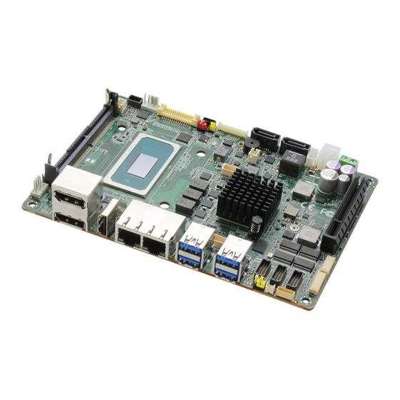
- Page 1 EPIC-TGH7 EPIC Board User’s Manual 1 Last Updated: August 8, 2022...
- Page 2 Copyright Notice This document is copyrighted, 2022. All rights are reserved. The original manufacturer reserves the right to make improvements to the products described in this manual at any time without notice. No part of this manual may be reproduced, copied, translated, or transmitted in any form or by any means without the prior written permission of the original manufacturer.
- Page 3 Acknowledgement All other products’ name or trademarks are properties of their respective owners. Microsoft Windows is a registered trademark of Microsoft Corp. ⚫ Intel®, Pentium®, and Celeron® are registered trademarks of Intel Corporation ⚫ Intel Atom™, Xeon™, and Core™ are trademarks of Intel Corporation ⚫...
- Page 4 Packing List Before setting up your product, please make sure the following items have been shipped: Item Quantity EPIC-TGH7 ⚫ Screw Kit ⚫ If any of these items are missing or damaged, please contact your distributor or sales representative immediately. Preface...
- Page 5 About this Document This User’s Manual contains all the essential information, such as detailed descriptions and explanations on the product’s hardware and software features (if any), its specifications, dimensions, jumper/connector settings/definitions, and driver installation instructions (if any), to facilitate users in setting up their product. Users may refer to the product page on AAEON.com for the latest version of this document.
- Page 6 Safety Precautions Please read the following safety instructions carefully. It is advised that you keep this manual for future references All cautions and warnings on the device should be noted. Make sure the power source matches the power rating of the device. Position the power cord so that people cannot step on it.
- Page 7 If any of the following situations arises, please the contact our service personnel: Damaged power cord or plug Liquid intrusion to the device iii. Exposure to moisture Device is not working as expected or in a manner as described in this manual The device is dropped or damaged Any obvious signs of damage displayed on the device...
- Page 8 FCC Statement This device complies with Part 15 FCC Rules. Operation is subject to the following two conditions: (1) this device may not cause harmful interference, and (2) this device must accept any interference received including interference that may cause undesired operation.
- Page 9 China RoHS Requirements (CN) 产品中有毒有害物质或元素名称及含量 AAEON Main Board/ Daughter Board/ Backplane 有毒有害物质或元素 部件名称 铅 汞 镉 六价铬 多溴联苯 多溴二苯醚 (Pb) (Hg) (Cd) (Cr(VI)) (PBB) (PBDE) 印刷电路板 × ○ ○ ○ ○ ○ 及其电子组件 外部信号 × ○ ○ ○ ○ ○ 连接器及线材...
- Page 10 China RoHS Requirement (EN) Poisonous or Hazardous Substances or Elements in Products AAEON Main Board/ Daughter Board/ Backplane Poisonous or Hazardous Substances or Elements Hexavalent Polybrominated Polybrominated Component Lead Mercury Cadmium Chromium Biphenyls Diphenyl Ethers (Pb) (Hg) (Cd) (Cr(VI)) (PBB) (PBDE) PCB &...
-
Page 11: Table Of Contents
Table of Contents Chapter 1 - Product Specifications..................1 Specifications ......................2 Chapter 2 – Hardware Information ..................5 Dimensions ....................... 6 Jumpers and Connectors ..................8 Block Diagram ......................10 List of Jumpers ......................11 2.4.1 Clear CMOS Jumper (JP6) ..............11 2.4.2 LVDS/eDP Port Backlight Inverter VCC Selection (JP2) .... - Page 12 2.5.12 FAN Connector (CN2 & 34) ..............30 2.5.13 eSPI Debug Port (CN24) ..............30 2.5.14 External Power Input (CN51) ..............31 2.5.15 ATX 12V Power Connector (CN7) ............31 2.5.16 USB 2.0 4 Port (On Board) (CN22) ............ 32 2.5.17 Front Panel (CN18) ................
- Page 13 3.4.2 Memory Configuration ................ 55 3.4.3 Hardware Monitor ................. 56 3.4.4 Smart Fan Mode Configuration ............57 3.4.5 PCH-FW Configuration ................ 60 3.4.6 Firmware Update Configuration............61 3.4.7 NVMe Configuration ................62 3.4.8 Power Management ................63 3.4.9 AAEON BIOS Robot ................64 3.4.10 Device Detecting Configuration ............
- Page 14 3.6.6 Serial Port Console Redirection ............90 3.6.7 Console Redirection Settings ............... 91 3.6.8 VMD Setup Menu.................. 93 3.6.9 PCH-IO Configuration ................95 Setup Submenu: Security ..................96 3.7.1 Trusted Computing ................97 3.7.2 Secure Boot .................... 99 3.7.3 Key Management ................100 Setup Submenu: Boot ..................
-
Page 15: Chapter 1 - Product Specifications
Chapter 1 Chapter 1 - Product Specifications... -
Page 16: Specifications
Specifications System Form Factor 4" EPIC Board 11th Generation Intel® Xeon™ / Core™ Processor CPU Frequency Xeon W-11865MRE (8C/16T, 2.60GHz, up to 4.70GHz) i7-11850HE (8C/16T, 2.60GHz, up to 4.70GHz) i5-11500HE (6C/12T, 2.60GHz, up to 4.50GHz) i3-11100HE (4C/8T, 2.40GHz, up to 4.40GHz) Celeron 6600HE (2C/2T, 2.60GHz) Chipset Intel®... - Page 17 System Operating Humidity 0% ~ 90% relative humidity, non-condensing MTBF (Hours) Certification CE/FCC Class A Display VGA/LCD Controller Intel® UHD Graphics for 11th Gen Intel® Processors Video Output Dual Channel 24/48bit LVDS (Default) or eDP x 1 HDMI2.0b x 1 DP 1.2a (DP++) x 2 VGA x 1 Backlight Inverter Supply...
- Page 18 Expansion Slot M.2 B-Key (3052) x 1 (Default PCIe [x1]+ USB 3.0+USB 2.0 , PCIe [x2]+ USB 2.0 by BOM) M.2 M-Key (2280) x 1 (PCIe 4.0 [x4]) PCIe 4.0 [x8] slot x 1 (Supply maximum 25W to the PCIe peripheral) Board to board FPC connector (PCIe [x4] x 1) 16-Bit TPM 2.0 (Optional)
-
Page 19: Chapter 2 - Hardware Information
Chapter 2 Chapter 2 – Hardware Information... -
Page 20: Dimensions
Dimensions Component Side Chapter 2 – Hardware Information... - Page 21 Solder Side Chapter 2 – Hardware Information...
-
Page 22: Jumpers And Connectors
Jumpers and Connectors Component Side Chapter 2 – Hardware Information... - Page 23 Solder Side Chapter 2 – Hardware Information...
-
Page 24: Block Diagram
Block Diagram Chapter 2 – Hardware Information... -
Page 25: List Of Jumpers
List of Jumpers The board features a number of jumpers which can be configured for your application. Please refer to the table below and following sections for all jumpers which can be configured. Label Function LVDS/eDP Backlight Lightness Control Mode Selection JP2 (1-2-3) LVDS/eDP Backlight Inverter VCC Selection JP2 (3-4-5) -
Page 26: Lvds/Edp Operating Vdd Selection (Jp2)
2.4.3 LVDS/eDP Operating VDD Selection (JP2) +3.3V(Default) 2.4.4 LVDS/eDP Port Backlight Lightness Control Mode Selection (JP1) 1 2 3 VR Mode (Default) PWM Mode 2.4.5 Touch Screen 4,5,8 Wire Selection (JP3) 4/8 Wires Mode (Default) 5 Wires Mode 2.4.6 Auto Power Button Enable/Disable Selection (JP5) 1 2 3 Disable Enable (Default) -
Page 27: List Of Connectors
List of Connectors This section details the connectors featured on the board, which can be configured for your application. For a list of mating connectors and cables, please see Appendix C. For Electrical Specifications of I/O Ports, please see Appendix D. Please refer to the table below for a list of all connectors on this board which can be configured. - Page 28 Label Function CN29-L I225 2.5G LAN CN29-R I219 Giga LAN CN31 USB 3.0 x 2 Connector (GEN2) CN32 USB 3.0 x 2 Connector (GEN2) CN33 Dual DP Connector CN34 FAN Connector CN38 PCIE FPC Connector CN39 Nano SIM CN40 DDR4 SODIMM1 CN41 Half Mini-Card/mSATA CN42...
-
Page 29: Vga Connector (Cn1)
2.5.1 VGA Connector (CN1) Pin Name Signal Type Signal Level VSYNC HSYNC DDC_CLK DDC_DATA BLUE GREEN Chapter 2 – Hardware Information... -
Page 30: Hdmi (Cn28)
2.5.2 HDMI (CN28) Pin Name Signal Type Signal Level HDMI_TX2+ DIFF HDMI_TX2- DIFF HDMI_TX1+ DIFF HDMI_TX1- DIFF HDMI_TX0+ DIFF HDMI_TX0- DIFF HDMI_CLK+ DIFF HDMI_CLK- DIFF DDC_CLK DDC_DATA Chapter 2 – Hardware Information... -
Page 31: Lvds/Edp (Cn6)
HDMI_HPD 2.5.3 LVDS/eDP (CN6) LVDS Pin Name Signal Type Signal level BKL_ENABLE BKL_ENABLE BKL_CONTROL BKL_CONTROL LCD_PWR LCD_PWR +3.3V/+5V LVDS_A_CLK- eDP_TXN3 DIFF LVDS_A_CLK+ eDP_TXP3 DIFF LCD_PWR LCD_PWR +3.3V/+5V LVDS_DA0- eDP_TXN2 DIFF LVDS_DA0+ eDP_TXP2 DIFF Chapter 2 – Hardware Information... - Page 32 LVDS_DA1- eDP_TXN1 DIFF LVDS_DA1+ eDP_TXP1 DIFF LVDS_DA2- eDP_TXN0 DIFF LVDS_DA2+ eDP_TXP0 DIFF LVDS_DA3- DIFF LVDS_DA3+ eDP_HPD DIFF DDC_DATA eDP_AUX_N +3.3V DDC_CLK eDP_AUX_P +3.3V LVDS_DB0- DIFF LVDS_DB0+ DIFF LVDS_DB1- DIFF LVDS_DB1+ DIFF LVDS_DB2- DIFF LVDS_DB2+ DIFF LVDS_DB3- DIFF LVDS_DB3+ DIFF LCD_PWR LCD_PWR +3.3V/+5V LVDS_B_CLK-...
-
Page 33: Lvds Port Inverter / Backlight Connector (Cn11)
2.5.4 LVDS Port Inverter / Backlight Connector (CN11) Pin Name Signal Type Signal Level BKL_PWR +5V / +12V BKL_PWR +5V / +12V BKL_CONTROL +3.3V BKL_ENABLE +3.3V Note: LVDS BKL_PWR can be set to +5V or +12V by JP2 (1-3-5). Note: LVDS BKL_CONTROL can be set by JP1. Chapter 2 –... -
Page 34: Mini-Card Slot (Half-Size) (Cn41)
2.5.5 Mini-Card Slot (Half-Size) (CN41) Pin Name Signal Type Signal Level PCIE_WAKE# +3.3VSB +3.3V +1.5V +1.5V PCIE_CLK_REQ# UIM_PWR UIM_DATA PCIE_REF_CLK- DIFF UIM_CLK PCIE_REF_CLK+ DIFF UIM_RST UIM_VPP W_DISABLE# +3.3V PCIE_RST# +3.3V PCIE_RX- DIFF +3.3VSB +3.3V Chapter 2 – Hardware Information... - Page 35 PCIE_RX+ DIFF +1.5V +1.5V SMB_CLK +3.3V PCIE_TX- DIFF SMB_DATA +3.3V PCIE_TX+ DIFF USB_D- DIFF USB_D+ DIFF +3.3VSB +3.3V +3.3VSB +3.3V +1.5V +1.5V +3.3VSB +3.3V Chapter 2 – Hardware Information...
-
Page 36: Sata Port (Cn4)
2.5.6 SATA Port (CN4) Pin Name Signal Type Signal Level SATA_TX+ DIFF SATA_TX- DIFF SATA_RX- DIFF SATA_RX+ DIFF Chapter 2 – Hardware Information... -
Page 37: Sata Port (Cn5)
2.5.7 SATA Port (CN5) Pin Name Signal Type Signal Level SATA_TX+ DIFF SATA_TX- DIFF SATA_RX- DIFF SATA_RX+ DIFF 2.5.8 M.2 M-Key Slot (2280) (CN43) Pin Name Signal Type Signal Level +3.3V +3.3V +3.3V +3.3V PCIE3_RX- DIFF PCIE3_RX+ DIFF Chapter 2 – Hardware Information... - Page 38 Pin Name Signal Type Signal Level SATA_LED +3.3V PCIE3_TX- +3.3V +3.3V PCIE3_TX+ +3.3V +3.3V +3.3V +3.3V PCIE2_RX- DIFF +3.3V +3.3V PCIE2_RX+ DIFF PCIE2_TX- DIFF PCIE2_TX+ DIFF PCIE1_RX- DIFF PCIE1_RX+ DIFF Chapter 2 – Hardware Information...
- Page 39 Pin Name Signal Type Signal Level PCIE1_TX- DIFF PCIE1_TX+ DIFF DECSLP PCIE0_RX- DIFF PCIE0_RX+ DIFF PCIE0_TX- DIFF PCIE0_TX+ DIFF PERST# PCIE_CLK_REQ# PCIE_CLK- DIFF PCIE_WAKE PCIE_CLK+ DIFF Chapter 2 – Hardware Information...
- Page 40 Pin Name Signal Type Signal Level +3.3V +3.3V +3.3V +3.3V +3.3V +3.3V Chapter 2 – Hardware Information...
-
Page 41: Lan (Rj-45) I225 (Left);I219 (Right) (Cn29)
2.5.9 LAN (RJ-45) I225 (Left);I219 (Right) (CN29) Pin Name Pin Name LAN2_MDI0_P LAN1_MDI0_P LAN2_MDI0_N LAN1_MDI0_N LAN2_MDI1_P LAN1_MDI1_P LAN2_MDI1_N LAN1_MDI1_N 1CT5 2CT5 1CT6 2CT6 LAN2_MDI2_P LAN1_MDI2_P LAN2_MDI2_N LAN1_MDI2_N LAN2_MDI3_P LAN1_MDI3_P 1P10 LAN2_MDI3_N 2P10 LAN1_MDI3_N LAN2_LED_LINK# LAN1_LED_LINK# LAN2_LED_3P3A LAN1_LED_3P3A LAN2_LED_2500# LAN1_LED_100# LAN2_LED_1000# LAN1_LED_1000# Chapter 2 –... -
Page 42: Usb Ports 1 & 2 (Cn31 & Cn32)
2.5.10 USB Ports 1 & 2 (CN31 & CN32) Pin Name Signal Type Signal Level +5VSB USB0_D- DIFF USB0_D+ DIFF USB0_SSRX− DIFF USB0_SSRX+ DIFF USB0_SSTX− DIFF USB0_SSTX+ DIFF +5VSB USB1_D- DIFF USB1_D+ DIFF USB1_SSRX− DIFF USB1_SSRX+ DIFF USB1_SSTX− DIFF USB1_SSTX+ DIFF Chapter 2 –... -
Page 43: Spi Flash Programming Port (Cn44)
2.5.11 SPI Flash Programming Port (CN44) Pin Name Signal Type Signal Level SPI_MISO SPI_CLK +3.3VSB +3.3V SPI_MOSI SPI_CS Chapter 2 – Hardware Information... -
Page 44: Fan Connector (Cn2 & 34)
2.5.12 FAN Connector (CN2 & 34) Pin Name Signal Type Signal Level +V12S +12V TACH 2.5.13 eSPI Debug Port (CN24) Pin Name Signal Type Signal Level ESPI_IO0_EC_R +3.3V ESPI_IO1_EC_R +3.3V ESPI_IO2_EC_R +3.3V ESPI_IO3_EC_R +3.3V +3.3V +3.3V ESPI_CS_EC_R_N +3.3V ESPI_RST_EC_R_N +3.3V ESPI_CLK_EC_R +3.3V SMB_DATA/I2C_SDA/3.3V... -
Page 45: External Power Input (Cn51)
2.5.14 External Power Input (CN51) Pin Name Signal Type Signal Level +VIN +12V 2.5.15 ATX 12V Power Connector (CN7) Standard ATX 12V Power Connector. Chapter 2 – Hardware Information... -
Page 46: Usb 2.0 4 Port (On Board) (Cn22)
2.5.16 USB 2.0 4 Port (On Board) (CN22) Pin Name Pin Name Pin 1 5V_USB Pin 2 5V_USB Pin 3 USB2_5_DN Pin 4 USB2_6_DN Pin 5 USB2_5_DP Pin 6 USB2_6_DP Pin 7 Pin 8 Pin 9 Pin 10 Pin 11 5V_USB Pin 12 5V_USB... -
Page 47: Output For Sata Hdd (Cn12)
2.5.18 +5V Output for SATA HDD (CN12) Pin Name Signal Type Signal Level 2.5.19 RTC Battery Connector (CN26) Pin Name Signal Type Signal Level +3.3V +3.3V Chapter 2 – Hardware Information... -
Page 48: Dio Port (Cn48)
2.5.20 DIO Port (CN48) Pin Name Pin Name Pin 1 Pin 2 Pin 3 DIO7_0 Pin 4 DIO8_0 Pin 5 DIO7_1 Pin 6 DIO8_1 Pin 7 DIO7_2 Pin 8 DIO8_2 Pin 9 DIO7_3 Pin 10 DIO8_3 Pin 11 DIO7_4 Pin 12 DIO8_4 Pin 13 DIO7_5... -
Page 49: Speaker Left (Cn13) / Speaker Right (Cn14)
2.5.21 Speaker Left (CN13) / Speaker Right (CN14) Pin Name Signal Type Signal Level AMP_OUT_L+ AMP_OUT_L- 2.5.22 External +5VSB Input (CN10) Pin Name Signal Type Signal Level PS_ON# +3.3V +5VSB Chapter 2 – Hardware Information... -
Page 50: Touch Screen Connector (Cn21)
2.5.23 Touch Screen Connector (CN21) 8 Wire Pin Name Signal Type Signal Level TOP EXCITE BOTTOM EXCITE LEFT EXCITE RIGHT EXCITE TOP SENSE BOTTOM SENSE LEFT SENSE RIGHT SENSE Note: 4/8 Wire and 5 Wire can be set by JP3. Chapter 2 –... - Page 51 4 Wire Pin Name Signal Type Signal Level BOTTOM LEFT RIGHT Note: 4/8 Wire and 5 Wire can be set by JP3. Chapter 2 – Hardware Information...
- Page 52 5 Wire Pin Name Signal Type Signal Level BOTTOM LEFT RIGHT Sense(S) Note: 4/8 Wire and 5 Wire can be set by JP3. Chapter 2 – Hardware Information...
-
Page 53: Audio I/O Port (Cn3)
2.5.24 Audio I/O Port (CN3) Pin Name Signal Type Signal Level RIGHT_OUT MIC_R LEFT_OUT MIC_L JD_LOUT JD_MIC GND_AUDIO GND_AUDIO JD_LIN LINE_R_IN +5V_AUDIO LINE_L_IN Chapter 2 – Hardware Information... -
Page 54: Nano Sim Card Socket (Cn39)
2.5.25 Nano SIM Card Socket (CN39) Pin Name Signal Type Signal Level UIM_PWR UIM_RST UIM_CLK UIM_VPP UIM_DATA Chapter 2 – Hardware Information... -
Page 55: Com Port 1/2 (Cn45)
2.5.26 COM Port 1/2 (CN45) RS232 Pin Name Signal Type Signal Level Port 1 Port 2 ±5V ±5V ±5V Chapter 2 – Hardware Information... - Page 56 RS422 Pin Name Signal Type Signal Level RS422_TX- ±5V RS422_TX+ ±5V RS422_RX+ RS422_RX- +5V/+12V(0.5A) +5V/+12V RS485 Pin Name Signal Type Signal Level RS485_ D- ±5V RS485_D+ ±5V +5V/+12V(0.5A) +5V/+12V Note: COM2 RS-232/422/485 can be set by BIOS setting. Default is RS-232. Note: Pin 8 function can be set by BOM.
-
Page 57: Com Port 3/4 (Cn46)
2.5.27 COM Port 3/4 (CN46) RS232 Pin Name Signal Type Signal Level Port 4 Port 3 ±9V ±9V ±9V Chapter 2 – Hardware Information... -
Page 58: Com Port 5/6 (Cn47)
2.5.28 COM Port 5/6 (CN47) RS232 Pin Name Signal Type Signal Level Port 6 Port 5 ±9V ±9V ±9V Chapter 2 – Hardware Information... -
Page 59: Dual Dp Port (Cn33)
2.5.29 Dual DP Port (CN33) Pin Name Signal Type Signal Level DP1_TX0_DP DIFF DP1_TX0_DN DIFF DP1_TX1_DP DIFF DP1_TX1_DN DIFF DP1_TX2_DP DIFF DP1_TX2_DN DIFF DP1_TX3_DP DIFF DP1_TX3_DN DIFF DP1_OB_AUX_EN DP1_AUX_DP DP1_AUX_DN HDMI_HPD1 +V3P3S +3.3V DP2_TX0_DP DIFF DP2_TX0_DN DIFF DP2_TX1_DP DIFF Chapter 2 – Hardware Information... -
Page 60: Ddr4 So-Dimm Slot (Cn40 & Cn17)
Pin Name Signal Type Signal Level DP2_TX1_DN DIFF DP2_TX2_DP DIFF DP2_TX2_DN DIFF DP2_TX3_DP DIFF DP2_TX3_DN DIFF DP2_OB_AUX_EN DP2_AUX_DP DP2_AUX_DN HDMI_HPD2 +V3P3S +3.3V 2.5.30 DDR4 SO-DIMM Slot (CN40 & CN17) Standard specification. 2.5.31 M.2 B-Key Slot (3052) (CN42) Standard specification. Chapter 2 – Hardware Information... -
Page 61: Pcie Fpc Connector (Cn38)
2.5.32 PCIE FPC Connector (CN38) Pin Name Signal Type Signal Level +V3P3S +3.3V +V3P3S +3.3V +V3P3S +3.3V SMB_DATA SMB_CLK BUF_PLT_RST# +V3P3A +3.3V PCIE_18_RXP DIFF PCIE_18_RXN DIFF PCIE_20_RXP DIFF PCIE_20_RXN DIFF PCIE_19_RXP DIFF PCIE_19_RXN DIFF PCIE_17_RXP DIFF PCIE_17_RXN DIFF PCIE_20_TXN DIFF PCIE_20_TXP DIFF PCIE_19_TXN... -
Page 62: Pcie X8 Slot (Cn16)
Pin Name Signal Type Signal Level PCIE_19_TXP DIFF PCIE_18_TXN DIFF PCIE_18_TXP DIFF CLK_PCIE_FPC_N DIFF CLK_PCIE_FPC_P DIFF PCIE_17_TXN DIFF PCIE_17_TXP DIFF +V12S +V12S +V12S +V12S +V12S 2.5.33 PCIE x8 Slot (CN16) Standard specification. Chapter 2 – Hardware Information... -
Page 63: Chapter 3 - Ami Bios Setup
Chapter 3 Chapter 3 - AMI BIOS Setup... -
Page 64: System Test And Initialization
System Test and Initialization These routines test and initialize board hardware. If the routines encounter an error during the tests, you will either hear a few short beeps or see an error message on the screen. There are two kinds of errors: fatal and non-fatal. The system can usually continue the boot up sequence with non-fatal errors. -
Page 65: Ami Bios Setup
AMI BIOS Setup AMI BIOS ROM has a built-in Setup program that allows users to modify the basic system configuration. This type of information is stored in battery-backed CMOS RAM and BIOS NVRAM so that it retains the Setup information when the power is turned off. Entering Setup Power on the computer and press <Del>or <ESC>... -
Page 66: Setup Submenu: Main
Setup Submenu: Main Chapter 3 – AMI BIOS Setup... -
Page 67: Setup Submenu: Advanced
Setup Submenu: Advanced Chapter 3 – AMI BIOS Setup... -
Page 68: Cpu Configuration
3.4.1 CPU Configuration Options Summary Intel (VMX) Disabled Virtualization Enabled Optimal Default, Failsafe Default Technology When enabled, a VMM can utilize the additional hardware capabilities provided by Vanderpool Technology. Intel(R) Disabled SpeedStep(tm) Enabled Optimal Default, Failsafe Default Allows more than two frequency ranges to be supported. Disabled Turbo Mode Enabled... -
Page 69: Memory Configuration
3.4.2 Memory Configuration Chapter 3 – AMI BIOS Setup... -
Page 70: Hardware Monitor
3.4.3 Hardware Monitor Options Summary Disabled Smart Fan Enabled Optimal Default, Failsafe Default Enable or Disable Smart Fan. Chapter 3 – AMI BIOS Setup... -
Page 71: Smart Fan Mode Configuration
3.4.4 Smart Fan Mode Configuration Options Summary Output PWM mode (push pull) FAN1 Output Linear Fan Application Mode Output PWM mode Optimal Default, Failsafe Default (open drain) Output PWM mode (push pull) to control 4-wire fans. Linear fan application circuit to control 3-wire fan speed by fan’s power terminal. - Page 72 Options Summary Auto fan speed control. Fan speed will follow Duty Cycle different temperature by different duty cycle Temperature 1-100 Options Summary Output PWM mode (push pull) FAN2 Output Linear Fan Application Mode Output PWM mode Optimal Default, Failsafe Default (open drain) Output PWM mode (push pull) to control 4-wire fans.
- Page 73 Options Summary CPU(PECI) Temperature Optimal Default, Failsafe Default Temperature System Temperature 2 Source System Temperature Select the monitored temperature source for this fan. Duty Cycle Auto fan speed control. Fan speed will follow different temperature by different Temperature duty cycle 1-100 Options Summary Manual Duty Optimal Default, Failsafe Default...
-
Page 74: Pch-Fw Configuration
3.4.5 PCH-FW Configuration Chapter 3 – AMI BIOS Setup... -
Page 75: Firmware Update Configuration
3.4.6 Firmware Update Configuration Options Summary Disabled Optimal Default, Failsafe Default Me FW Image Re-Flash Enabled Enable/Disable Me FW Image Re-Flash function. Disabled FW Update Enabled Optimal Default, Failsafe Default Enable/Disable ME FW Update function. Chapter 3 – AMI BIOS Setup... -
Page 76: Nvme Configuration
3.4.7 NVMe Configuration Chapter 3 – AMI BIOS Setup... -
Page 77: Power Management
3.4.8 Power Management Options Summary ATX Type Optimal Default, Failsafe Default Power Mode AT Type Select system power mode. Last State Optimal Default, Failsafe Default Restore AC Power Always On Loss Always Off IO Restore AC power Loss. Disable Optimal Default, Failsafe Default RTC wake system Fixed Time from S5... -
Page 78: Aaeon Bios Robot
3.4.9 AAEON BIOS Robot Options Summary Disabled Optimal Default, Failsafe Default Sends watch dog before BIOS POST Enabled Enabled - Robot set Watch Dog Timer (WDT) right after power on, before BIOS start POST process. And then Robot will clear WDT on completion of POST. WDT will reset system automatically if it is not cleared before its timer counts down to zero. - Page 79 Enabled - Robot set Watch Dog Timer (WDT) after POST completion, before BIOS transfer control to OS. WARNING: Before enabling this function, a program in OS must be in responsible for clearing WDT. Also, this function should be disabled if OS is going to update itself.
-
Page 80: Device Detecting Configuration
3.4.10 Device Detecting Configuration Options Summary Action Reset System Optimal Default, Failsafe Default Hold System Select action that robot should do. Soft or hard reset Soft Optimal Default, Failsafe Default Hard Select reset type robot should send on each boot. Retry-Count Optimal Default, Failsafe Default Fill retry counter here. - Page 81 Options Summary Action Reset System Optimal Default, Failsafe Default Hold System Select action that robot should do. Holding time out Optimal Default, Failsafe Default (second) Fill hold time out here. Robot will hold system no longer then time-out value, and then let system continue its POST.
-
Page 82: Device #* Detecting Configuration - Interface
3.4.10.1 Device #* Detecting Configuration – Interface Options Summary Interface Disabled Optimal Default, Failsafe Default SMBUS Legacy I/O Super I/O MMIO Select interface robot should use to communicate with device. Chapter 3 – AMI BIOS Setup... -
Page 83: Device #* Detecting Configuration - Pci
3.4.10.2 Device #* Detecting Configuration – PCI Options Summary When interface item set to "PCI" will show below items Optimal Default, Failsafe Default Fill BUS number to a PCI device, in hexadecimal. Range: 0 – FF. Device Optimal Default, Failsafe Default Fill DEVICE number to a PCI device, in hexadecimal. - Page 84 Register data is bitwise equal to Optimal Default, Failsafe Default bytewise equal to bytewise lesser than bytewise larger than Select how robot should compare data read from register, to a value configured below. Register offset Optimal Default, Failsafe Default Fill register offset (or index) for robot to read, in hexadecimal. Range: 0 - FF Bit offset Optimal Default, Failsafe Default Fill bit offset for register, for robot to compare with bit value.
-
Page 85: Device #* Detecting Configuration - Dio
3.4.10.3 Device #* Detecting Configuration – DIO Options Summary When interface item set to "DIO" will show below items Device Is not Optimal Default, Failsafe Default Select that robot should or should not do action if condition met. DIO pin number DIO1 Optimal Default, Failsafe Default DIO*... -
Page 86: Device #* Detecting Configuration - Smbus
3.4.10.4 Device #* Detecting Configuration – SMBUS Options Summary When interface item set to "SMBUS" will show below items SMBUS Slave Optimal Default, Failsafe Default Address Fill slave address to a SMBUS device, in hexadecimal. Range: 0 - FF Device Is not Optimal Default, Failsafe Default Select that robot should or should not do action if condition met. -
Page 87: Device #* Detecting Configuration - Legacy I/O
Register data is bitwise equal to Optimal Default, Failsafe Default bytewise equal to bytewise lesser than bytewise larger than Select how robot should compare data read from register, to a value configured below. Register offset Optimal Default, Failsafe Default Fill register offset (or index) for robot to read, in hexadecimal. Range: 0 – FF. Bit offset Optimal Default, Failsafe Default Fill bit offset for register, for robot to compare with bit value. - Page 88 Options Summary When interface item set to "Legacy I/O" will show below items I/O Address Optimal Default, Failsafe Default Fill I/O address device is responding to. Range: 0~FFFF. Device Is not Optimal Default, Failsafe Default Select that robot should or should not do action if condition met. In condition Present Optimal Default, Failsafe Default...
-
Page 89: Device #* Detecting Configuration - Super I/O
3.4.10.6 Device #* Detecting Configuration – Super I/O Options Summary When interface item set to "Super I/O" will show below items Super I/O LDN Optimal Default, Failsafe Default Fill LDN number to a Super I/O device. Range: 0~FF. Device Is not Optimal Default, Failsafe Default Select that robot should or should not do action if condition met. - Page 90 Select how robot should compare data read from register, to a value configured below. Register offset Optimal Default, Failsafe Default Fill register offset (or index) for robot to read, in hexadecimal. Range: 0 - FF Bit offset Optimal Default, Failsafe Default Fill bit offset for register, for robot to compare with bit value.
-
Page 91: Device #* Detecting Configuration - Mmio
3.4.10.7 Device #* Detecting Configuration – MMIO Options Summary When interface item set to "MMIO" will show below items MMIO Address Optimal Default, Failsafe Default Fill Memory Mapped I/O address device is responding to. Range: 0~FFFFFFFF. Device Is not Optimal Default, Failsafe Default Select that robot should or should not do action if condition met. -
Page 92: Setup Submenu: System I/O
Select how robot should compare data read from register, to a value configured below. Bit offset Optimal Default, Failsafe Default Fill bit offset for register, for robot to compare with bit value. Bit value Optimal Default, Failsafe Default High Fill bit value for robot to compare register-bit with specified offset. Byte value Optimal Default, Failsafe Default Fill a byte value for robot to compare register data with, in hexadecimal. -
Page 93: Pci Express Configuration
3.6.1 PCI Express Configuration Options Summary PCI Express Root Enabled Optimal Default, Failsafe Default Port 16 (CN41) Disabled Control the PCI Express Root Port. Chapter 3 – AMI BIOS Setup... -
Page 94: Storage Configuration
3.6.2 Storage Configuration Options Summary SATA Controller(s) Disabled Enabled Optimal Default, Failsafe Default Enable/Disable SATA Device. Port 0 Disabled Enabled Optimal Default, Failsafe Default Enable or Disable SATA Port. Hot Plug Disabled Optimal Default, Failsafe Default Enabled Designates this port as Hot Pluggable. Port 1 Disabled Enabled... -
Page 95: Hd Audio Subsystem Configuration Settings
3.6.3 HD Audio Subsystem Configuration Settings Options Summary HD Audio Disabled Enabled Optimal Default, Failsafe Default Control Detection of the HD-Audio device. Disabled = HDA will be unconditionally disabled. Enabled = HDA will be unconditionally enabled. Chapter 3 – AMI BIOS Setup... -
Page 96: Hd Audio Subsystem Configuration Settings
3.6.4 HD Audio Subsystem Configuration Settings Options Summary DIO Port* Output Input Set DIO as Input or Output. Output Level High Optimal Default, Failsafe Default Set output level when DIO pin is output. Chapter 3 – AMI BIOS Setup... -
Page 97: Legacy Logical Devices Configuration
3.6.5 Legacy Logical Devices Configuration Chapter 3 – AMI BIOS Setup... -
Page 98: Serial Port 1 Configuration
3.6.5.1 Serial Port 1 Configuration Options Summary Use This Device Disable Enable Optimal Default, Failsafe Default Enable or Disable this Logical Device. Possible: Use Automatic Settings Optimal Default, Failsafe Default IO=3F8h; IRQ=4 IO=2F8h; IRQ=3 Allows user to change Device's Resource settings. New settings will be reflected on This Setup Page after System restarts. -
Page 99: Serial Port 2 Configuration
3.6.5.2 Serial Port 2 Configuration Options Summary Use This Device Disable Enable Optimal Default, Failsafe Default Enable or Disable this Logical Device. Possible: Use Automatic Settings Optimal Default, Failsafe Default IO=2F8h; IRQ=3 IO=3F8h; IRQ=4 Allows user to change Device's Resource settings. New settings will be reflected on This Setup Page after System restarts. -
Page 100: Serial Port 3 Configuration
3.6.5.3 Serial Port 3 Configuration Options Summary Use This Device Disable Enable Optimal Default, Failsafe Default Enable or Disable this Logical Device. Possible: Use Automatic Settings Optimal Default, Failsafe Default IO=2F8h; IRQ=3 IO=3F8h; IRQ=4 Allows user to change Device's Resource settings. New settings will be reflected on This Setup Page after System restarts. -
Page 101: Serial Port 4 Configuration
3.6.5.4 Serial Port 4 Configuration Options Summary Use This Device Disable Enable Optimal Default, Failsafe Default Enable or Disable this Logical Device. Possible: Use Automatic Settings Optimal Default, Failsafe Default IO=2F8h; IRQ=3 IO=3F8h; IRQ=4 Allows user to change Device's Resource settings. New settings will be reflected on This Setup Page after System restarts. -
Page 102: Serial Port 5 Configuration
3.6.5.5 Serial Port 5 Configuration Options Summary Use This Device Disable Enable Optimal Default, Failsafe Default Enable or Disable this Logical Device. Possible: Use Automatic Settings Optimal Default, Failsafe Default IO=2F8h; IRQ=3 IO=3F8h; IRQ=4 Allows user to change Device's Resource settings. New settings will be reflected on This Setup Page after System restarts. -
Page 103: Serial Port 6 Configuration
3.6.5.6 Serial Port 6 Configuration Options Summary Use This Device Disable Enable Optimal Default, Failsafe Default Enable or Disable this Logical Device. Possible: Use Automatic Settings Optimal Default, Failsafe Default IO=2F8h; IRQ=3 IO=3F8h; IRQ=4 Allows user to change Device's Resource settings. New settings will be reflected on This Setup Page after System restarts. -
Page 104: Serial Port Console Redirection
3.6.6 Serial Port Console Redirection Options Summary Console Redirection Disabled Optimal Default, Failsafe Default Enabled Console Redirection Enable or Disable. Console Redirection Disabled Optimal Default, Failsafe Default Enabled Console Redirection Enable or Disable. Chapter 3 – AMI BIOS Setup... -
Page 105: Console Redirection Settings
3.6.7 Console Redirection Settings Options Summary Terminal Type VT100 VT100+ VT-UTF8 ANSI Optimal Default, Failsafe Default Emulation: ANSI: Extended ASCII char set. VT100: ASCII char set. VT100+: Extends VT100 to support color, function keys, etc. VT-UTF8: Uses UTF8 encoding to map Unicode chars onto 1 or more bytes. - Page 106 Data Bits Optimal Default, Failsafe Default Parity None Optimal Default, Failsafe Default Even Mark Space A parity bit can be sent with the data bits to detect some transmission errors. Even: parity bit is 0 if the num of 1's in the data bits is even. Odd: parity bit is 0 if num of 1's in the data bits is odd.
-
Page 107: Vmd Setup Menu
3.6.8 VMD Setup Menu Options Summary Enable VMD Disabled Optimal Default, Failsafe Default controller Enabled Enable/Disable to VMD controller. Chapter 3 – AMI BIOS Setup... - Page 108 Options Summary Enable VMD Global Disabled Optimal Default, Failsafe Default Mapping Enabled Enable/Disable to VMD Global Mapping. Map this Root Port Disabled under VMD Enabled Optimal Default, Failsafe Default Map/UnMap this Root Port to VMD. RAID0 Disabled Enabled Optimal Default, Failsafe Default Enable/Disable RAID0 support".
-
Page 109: Pch-Io Configuration
Intel Rapid Recovery Disabled Technology Enabled Optimal Default, Failsafe Default Enable/Disable Intel Rapid Recovery Technology. RRT volumes can Disabled span internal and Enabled Optimal Default, Failsafe Default eSATA drives Enable/Disable RRT volumes can span internal and eSATA drives. Intel(R) Optane(TM) Disabled Memory Enabled... -
Page 110: Setup Submenu: Security
Setup Submenu: Security Change User/Supervisor Password You can install a Supervisor password, and if you install a supervisor password, you can then install a user password. A user password does not provide access to many of the features in the Setup utility. If you highlight these items and press Enter, a dialog box appears which lets you enter a password. -
Page 111: Trusted Computing
3.7.1 Trusted Computing Options Summary Security Device Disable Support Enable Optimal Default, Failsafe Default Enables or Disables BIOS support for security device. O.S. will not show Security Device. TCG EFI protocol and INT1A interface will not be available. SHA-1 PCR Bank Disable Enable Optimal Default, Failsafe Default... - Page 112 Platform Hierarchy Disabled Enabled Optimal Default, Failsafe Default Enable or disable Platform Hierarchy. Storage Hierarchy Disabled Enabled Optimal Default, Failsafe Default Enable or Disable Storage Hierarchy. Endorsement Disabled Hierarchy Enabled Optimal Default, Failsafe Default Enable or Disable Endorsement Hierarchy. TPM2.0 UEFI Spec TCG_1_2 Version TCG_2...
-
Page 113: Secure Boot
3.7.2 Secure Boot Options Summary Secure Boot Disabled Optimal Default, Failsafe Default Enabled Secure Boot feature is Active if Secure Boot is Enabled, Platform Key (PK) is enrolled and the System is in User mode. The mode change requires platform reset. Secure Boot Mode Custom Optimal Default, Failsafe Default Standard... -
Page 114: Key Management
3.7.3 Key Management Options Summary Factory Key Disabled Optimal Default, Failsafe Default Provision Enabled Secure Boot feature is Active if Secure Boot is Enabled, Platform Key (PK) is enrolled and the System is in User mode. The mode change requires platform reset. Restore Factory Keys Force System to User Mode. - Page 115 Remove 'UEFI CA' from DB Device Guard ready system must not list 'Microsoft UEFI CA' Certificate in Authorized Signature database (db). Restore DB defaults Restore DB variable to factory defaults. Platform Key (PK) Details Export Update Delete Key Exchange Keys Details Export Update...
-
Page 116: Setup Submenu: Boot
Setup Submenu: Boot Options Summary Quiet Boot Disabled Enabled Optimal Default, Failsafe Default Enable/Disable showing boot logo. Lunch PXE ROM Disabled Optimal Default, Failsafe Default Enabled Enable/Disable UEFI Network Stack. Chapter 3 – AMI BIOS Setup... -
Page 117: Bbs Priorities
3.8.1 BBS Priorities Chapter 3 – AMI BIOS Setup... -
Page 118: Setup Submenu: Save & Exit
Setup Submenu: Save & Exit Chapter 3 – AMI BIOS Setup... -
Page 119: Chapter 4 - Drivers Installation
Chapter 4 Chapter 4 – Drivers Installation... -
Page 120: Drivers Download And Installation
Drivers Download and Installation Drivers for the EPIC-TGH7 can be downloaded from the product page on the AAEON website by following this link: https://www.aaeon.com/en/p/epic-boards-epic-tgh7 Download the driver(s) you need and follow the steps below to install them. Step 1 – Install Chipset Drivers Open the Step 1 –... - Page 121 Step 4 – Install Audio Driver Open the Step 4 – Audio folder Open the Setup.exe file Follow the instructions Drivers will be installed automatically Step 5 – Install Peripheral Driver Open the Step 5 – Peripheral Driver folder Open the SetupSerialIO.exe file Follow the instructions Drivers will be installed automatically Step 6 –...
-
Page 122: Appendix A - I/O Information
Appendix A Appendix A – I/O Information... -
Page 123: I/O Address Map
I/O Address Map Appendix A – I/O Information... -
Page 124: A.2 Memory Address Map
A.2 Memory Address Map Appendix A – I/O Information... -
Page 125: A.3 Irq Mapping Chart
A.3 IRQ Mapping Chart Appendix A – I/O Information... - Page 126 Appendix A – I/O Information...
- Page 127 Appendix A – I/O Information...
-
Page 128: Appendix B - Mating Connectors
Appendix B Appendix B – Mating Connectors... -
Page 129: List Of Mating Connectors And Cables
List of Mating Connectors and Cables Mating Connector Con. Available Function Cable P/N Label Cable Vendor Model no VGA cable Molex 510211300 1709150151 Connector 15cm Molex 22-01-2045 Audio 50247-012H0H0 Audio Cable 170X000156 ACES Connector -001 25cm 170X000517 SATA SATA Cable Molex 887505318 1709070150... - Page 130 Mating Connector Con. Available Function Cable P/N Label Cable Vendor Model no COM Port 1&2 50247-020H0 Dual COM CN45 (RS232/422/48 Aces 170X000231 H0-001 cable 30cm COM Port 3&4 50247-020H0 Dual COM CN46 Aces 170X000231 (RS232 Only) H0-001 cable 30cm COM Port 5&6 50247-020H0 Dual COM CN47...
-
Page 131: Appendix C - 3-Pin Atx Behavior Description
Appendix C Appendix C – 3-Pin ATX Behavior Description... -
Page 132: 3-Pin Atx Behavior Description
3-Pin ATX Behavior Description For board level power design, the EPIC-TGH7 supports the 3-Pin ATX Power Scheme, and there are 3 scenarios. Single Input Power Source – AT mode Operate as “AT” mode, which the HW design supports “Auto Power Button: Enable” Case 1: When power supply or power adapter is “powered”, the system will boot up. - Page 133 Single Input Power Source – ATX mode Operating in “ATX mode”, wherein the H/W auto power button sets: disable, you must manually trigger the power button signal in order to power up or turn off the system. In this mode, when the power supply or power source is “powered”, manually trigger the PWRBTN# signal to turn on or shut down the system.
- Page 134 12V Input Power with 3-pin ATX External Connector Operating in “ATX mode”, manually triggering PWRBTN# is necessary to power up or shut down the system. All peripherals are powered by the S-rail powers, and S-rail powers (such as +12V and +5V), so they will power on or off with the power source. Pin Name Signal Type Signal Level...
-
Page 135: Atx Power Table
ATX Power Table Power Supply Power Supply Type Unit / Turn On Unit / Turn Off Powered No Power Mainboard Single Input Power Source - AT Mode External Powered Powered Peripherals Powered No Power Mainboard Single Input Power Source - ATX Mode External Powered...
Need help?
Do you have a question about the AAEON EPIC-TGH7 and is the answer not in the manual?
Questions and answers