Table of Contents
Advertisement
Quick Links
Advertisement
Table of Contents

Related Manuals for Asus Aaeon EPIC-BT07


Summary of Contents for Asus Aaeon EPIC-BT07
- Page 1 EPIC-BT07 EPIC Board User’s Manual 8 Last Updated: August 12, 2022...
- Page 2 Copyright Notice This document is copyrighted, 2022. All rights are reserved. The original manufacturer reserves the right to make improvements to the products described in this manual at any time without notice. No part of this manual may be reproduced, copied, translated, or transmitted in any form or by any means without the prior written permission of the original manufacturer.
- Page 3 Acknowledgement All other products’ name or trademarks are properties of their respective owners. Microsoft Windows is a registered trademark of Microsoft Corp. ⚫ Intel®, Pentium®, and Celeron® are registered trademarks of Intel Corporation ⚫ Intel Atom™ is a trademark of Intel Corporation ⚫...
- Page 4 Packing List Before setting up your product, please make sure the following items have been shipped: Item Quantity EPIC-BT07 ⚫ SATA Cable ⚫ SATA Power Cable ⚫ Heat-Spreader ⚫ If any of these items are missing or damaged, please contact your distributor or sales representative immediately.
- Page 5 About this Document This User’s Manual contains all the essential information, such as detailed descriptions and explanations on the product’s hardware and software features (if any), its specifications, dimensions, jumper/connector settings/definitions, and driver installation instructions (if any), to facilitate users in setting up their product. Users may refer to the product page on AAEON.com for the latest version of this document.
- Page 6 Safety Precautions Please read the following safety instructions carefully. It is advised that you keep this manual for future references All cautions and warnings on the device should be noted. Make sure the power source matches the power rating of the device. Position the power cord so that people cannot step on it.
- Page 7 If any of the following situations arises, please the contact our service personnel: Damaged power cord or plug Liquid intrusion to the device iii. Exposure to moisture Device is not working as expected or in a manner as described in this manual The device is dropped or damaged Any obvious signs of damage displayed on the device...
- Page 8 FCC Statement This device complies with Part 15 FCC Rules. Operation is subject to the following two conditions: (1) this device may not cause harmful interference, and (2) this device must accept any interference received including interference that may cause undesired operation.
- Page 9 China RoHS Requirements (CN) 产品中有毒有害物质或元素名称及含量 AAEON Main Board/ Daughter Board/ Backplane 有毒有害物质或元素 部件名称 铅 汞 镉 六价铬 多溴联苯 多溴二苯醚 (Pb) (Hg) (Cd) (Cr(VI)) (PBB) (PBDE) 印刷电路板 × ○ ○ ○ ○ ○ 及其电子组件 外部信号 × ○ ○ ○ ○ ○ 连接器及线材...
- Page 10 China RoHS Requirement (EN) Poisonous or Hazardous Substances or Elements in Products AAEON Main Board/ Daughter Board/ Backplane Poisonous or Hazardous Substances or Elements Hexavalent Polybrominated Polybrominated Component Lead Mercury Cadmium Chromium Biphenyls Diphenyl Ethers (Pb) (Hg) (Cd) (Cr(VI)) (PBB) (PBDE) PCB &...
-
Page 11: Table Of Contents
Table of Contents Chapter 1 - Product Specifications..................1 Specifications ......................2 Chapter 2 – Hardware Information ..................4 Dimensions ....................... 5 Jumpers and Connectors ..................7 Block Diagram ......................9 List of Jumpers ......................10 2.4.1 Auto Power Button Selection (CN3) ........... 10 2.4.2 PCI-104 VI/O Voltage Selection (CN4) .......... - Page 12 2.5.7 Audio Connector (CN10) ..............19 2.5.8 LPT/ Digital I/O Connector (CN12) ............ 20 2.5.9 USB 2.0 Port 2/3/4/5 (CN13/14/15/16) ..........22 2.5.10 LVDS/eDP Inverter / Backlight Connector (CN19) ......23 2.5.11 MicroSD Card Connector (CN20) ............24 2.5.12 LPC Expansion Connector (CN21) ............25 2.5.13 UIM Socket (CN22) ................
- Page 13 Chapter 3 - AMI BIOS Setup ....................57 System Test and Initialization ................58 AMI BIOS Setup ..................... 59 Setup Submenu: Main ..................60 Setup Submenu: Advanced .................. 61 3.4.1 CPU Configuration ................62 3.4.2 IDE Configuration .................. 63 3.4.3 USB Configuration .................
- Page 14 Setup Submenu: Save & Exit ................87 Chapter 4 – Drivers Installation .................... 88 Drivers Download and Installation ..............89 Appendix A – I/O Information .................... 100 I/O Address Map ....................101 Memory Address Map ..................103 IRQ Mapping Chart ..................... 104 Appendix B –...
-
Page 15: Chapter 1 - Product Specifications
Chapter 1 Chapter 1 - Product Specifications... -
Page 16: Specifications
Specifications System Form Factor 4” EPIC Board Intel® Atom™ E3845/Celeron® J1900/N2807 CPU Frequency Up to 2.0 GHz Chipset Intel® Atom™/ Celeron® SoC Memory Type DDR3L 1333, SODIMM x 1 Max. Memory Capacity Up to 8G BIOS Wake on LAN Watchdog Timer 255 Levels Power Requirement +12V or 9-24V AT/ATX (default) - Page 17 Ethernet Intel® i211 Gigabit Ethernet, RJ-45 x 2 Audio High Definition Audio Interface USB Port USB2.0 x 5 USB3.2 Gen 1 x 1 Serial Port RS-232 x 4 (COM1, COM4, COM5, COM6) RS-232/422/485 x 1 (Ring/ +5V/ +12V) (COM2, COM3) Parallel Port SPP/EPP/ECP x 1 HDD Interface...
-
Page 18: Chapter 2 - Hardware Information
Chapter 2 Chapter 2 – Hardware Information... -
Page 19: Dimensions
Dimensions Component Side Chapter 2 – Hardware Information... - Page 20 Solder Side Chapter 2 – Hardware Information...
-
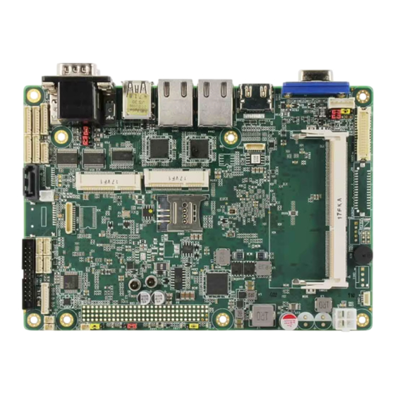
Page 21: Jumpers And Connectors
Jumpers and Connectors Component Side Component Side Chapter 2 – Hardware Information... - Page 22 Solder Side Chapter 2 – Hardware Information...
-
Page 23: Block Diagram
Block Diagram Chapter 2 – Hardware Information... -
Page 24: List Of Jumpers
List of Jumpers The board features a number of jumpers which can be configured for your application. Please refer to the table below and following sections for all jumpers which can be configured. Label Function Auto Power Button Selection PCI-104 VIO Voltage Selection CMOS RTC Setting CN17 LVDS/ eDP Backlight Voltage Selection... -
Page 25: Vi/O Voltage Selection (Cn4)
2.4.2 PCI-104 VI/O Voltage Selection (CN4) +3.3V (Default) 2.4.3 CMOS RTC Setting (CN5) Normal (Default) Clear CMOS 2.4.4 LVDS/eDP Backlight Voltage Selection (CN17) +12V +5V (Default) 2.4.5 LVDS/eDP Backlight Control Selection (CN18) VR Mode (Default) PWM Mode Chapter 2 – Hardware Information... -
Page 26: Touchscreen 4/5/8-Wire Mode Selection (Cn28)
2.4.6 Touchscreen 4/5/8-wire Mode Selection (CN28) 4/8 Wires Mode (Default) 5 Wires Mode 2.4.7 COM2 RI/+5/+12V Selection (CN34) +12V Ring (Default) 2.4.8 COM3 RI/+5/+12V Selection (CN36) +12V Ring (Default) 2.4.9 eDP Operating Voltage Selection (CN40) +3.3V (Default) Chapter 2 – Hardware Information... -
Page 27: Lvds/Edp Operating Voltage Selection (Cn41)
2.4.10 LVDS/eDP Operating Voltage Selection (CN41) +3.3V (Default) 2.4.11 eDP Backlight Control Selection (CN42) VR Mode (Default) PWM Mode 2.4.12 eDP Backlight Voltage Selection (CN43) +12V +5V (Default) Chapter 2 – Hardware Information... -
Page 28: List Of Connectors
List of Connectors This section details the connectors featured on the board, which can be configured for your application. For a list of mating connectors and cables, please see Appendix C. For Electrical Specifications of I/O Ports, please see Appendix D. Please refer to the table below for a list of all connectors on this board which can be configured. - Page 29 Label Function CN27 Mini-Card / mSATA Slot CN29 Touch Screen Connector CN30 PS/2 Keyboard Mouse Connector CN31 COM Port 6 CN32 COM Port 5 CN33 SPI Programming Port CN35 LVDS/eDP Port CN37 COM Port 4 CN38 COM Port 3 CN39 Front Panel Connector CN44 10/100/1000 Mbps Ethernet Port 1...
-
Page 30: Stereo Audio Right Channel (Cn1)
2.5.1 Stereo Audio Right Channel (CN1) Pin Name Signal Type Signal Level 2.5.2 RTC Battery Connector (CN2) Pin Name Signal Type Signal Level +3.3 V 3.3 V 2.5.3 4-Pin Power-In Connector (CN6) Pin Name Signal Type Signal Level +VIN +12V // +9V to +24V +VIN +12V // +9V to +24V Chapter 2 –... -
Page 31: Stereo Audio Left Channel (Cn7)
2.5.4 Stereo Audio Left Channel (CN7) Pin Name Signal Type Signal Level 2.5.5 2-Pin Power in Connector (CN8) Pin Name Signal Type Signal Level +VIN +12V // +9V to +24V 2.5.6 PCI-104 Connector (CN9) +5V_SB AD00 VI/O AD02 AD01 AD05 AD04 AD03 C/BE0#... - Page 32 +3.3V C/BE1# AD15 +3.3V SERR# PSON# PERR# +3.3V PME# STOP# +3.3V LOCK# +3.3V TRDY# DEVSEL# FRAME# IRDY# +3.3V AD16 +3.3V C/BE2# AD18 +3.3V AD17 AD21 AD20 AD19 +3.3V AD23 AD22 +3.3V IDSEL0 IDSEL1 IDSEL2 AD24 C/BE3# VI/O IDSEL3 AD26 AD25 AD29 AD28 AD27...
-
Page 33: Audio Connector (Cn10)
2.5.7 Audio Connector (CN10) Pin Name Signal Type Signal Level MIC_L MIC_R GND_AUDIO LINE_L_IN LINE_R_IN GND_AUDIO LEFT_OUT GND_AUDIO RIGHT_OUT +5V_AUDIO Chapter 2 – Hardware Information... -
Page 34: Lpt/ Digital I/O Connector (Cn12)
2.5.8 LPT/ Digital I/O Connector (CN12) LPT Mode: Pin Name Signal Type Signal Level STOBE# #AFD PPD0 ERR# PPD1 PINIT# PPD2 SLIN# PPD3 PPD4 PPD5 PPD6 PPD7 ACK# BUSY Chapter 2 – Hardware Information... - Page 35 Pin Name Signal Type Signal Level SLCT Digital I/O Mode: Pin Name Signal Type Signal Level GPIO15 GPIO14 GPIO0 GPIO13 GPIO1 GPIO12 GPIO2 GPIO11 GPIO3 GPIO4 GPIO5 GPIO6 GPIO7 Chapter 2 – Hardware Information...
-
Page 36: Usb 2.0 Port 2/3/4/5 (Cn13/14/15/16)
Pin Name Signal Type Signal Level GPIO10 GPIO9 GPIO8 2.5.9 USB 2.0 Port 2/3/4/5 (CN13/14/15/16) Pin Name Signal Type Signal Level +5VSB USB2_D- DIFF USB2_D+ DIFF Chapter 2 – Hardware Information... -
Page 37: Lvds/Edp Inverter / Backlight Connector (Cn19)
2.5.10 LVDS/eDP Inverter / Backlight Connector (CN19) Notes: BLK_PWR can be set to +12V or+5V by jumper CN17 (see section 2.4.4). The maximum driving current is 1.5A. BLK_CONTROL can be set to VR Mode or PWM Mode by jumper CN18 (see section 2.4.5) Pin Name Signal Type... -
Page 38: Microsd Card Connector (Cn20)
2.5.11 MicroSD Card Connector (CN20) Pin Name Signal Type Signal Level SDIO_D2 SDIO_D3 SDIO_CMD +3.3V +3.3V SDIO_CLK SDIO_D0 SDIO_D1 SDIO_CD# Chapter 2 – Hardware Information... -
Page 39: Lpc Expansion Connector (Cn21)
2.5.12 LPC Expansion Connector (CN21) Pin Name Signal Type Signal Level LAD0 +3.3V LAD1 +3.3V LAD2 +3.3V LAD3 +3.3V +3.3V +3.3V LFRAME# LRESET# +3.3V LCLK SERIRQ +3.3V Chapter 2 – Hardware Information... -
Page 40: Uim Socket (Cn22)
2.5.13 UIM Socket (CN22) Pin Name Signal Type Signal Level UIM_PWR UIM_RST UIM_CLK UIM_VPP UIM_DATA 2.5.14 +5V Output for SATA HDD (CN23) Pin Name Signal Type Signal Level Chapter 2 – Hardware Information... -
Page 41: Edp (Cn24)
2.5.15 eDP (CN24) Notes: LVDS LCD_PWR can be set to +3.3V or +5V by CN40 (see section 2.4.9). The max driving current is 2A. Pin Name Signal Type Signal Level BKL_ENABLE BKL_CONTROL LCD_PWR +3.3V/+5V eDP_DA3- DIFF eDP_DA3+ DIFF LCD_PWR +3.3V/+5V Chapter 2 –... - Page 42 Pin Name Signal Type Signal Level eDP_DA2- DIFF eDP_DA2+ DIFF eDP_DA1- DIFF eDP_DA1+ DIFF eDP_DA0- DIFF eDP_DA0+ DIFF Hot Plug Detect # eDP_AUX- DIFF eDP_AUX+ DIFF LCD_PWR +3.3V/+5V Chapter 2 – Hardware Information...
-
Page 43: Sata Port1 (Cn25)
2.5.16 SATA Port1 (CN25) Pin Name Signal Type Signal Level SATA_TX+ DIFF SATA_TX- DIFF SATA_RX- DIFF SATA_RX+ DIFF 2.5.17 MiniCard Slot (CN26) Pin Name Signal Type Signal Level PCIE_WAKE# +3.3VSB +3.3V +1.5V +1.5V PCIE_CLK_REQ# UIM_PWR UIM_DAT Chapter 2 – Hardware Information... - Page 44 Pin Name Signal Type Signal Level PCIE_REF_CLK- DIFF UIM_CLK PCIE_REF_CLK+ DIFF UIM_RST UIM_VPP W_DISABLE# +3.3V PCIE_RST# +3.3V PCIE_RX- DIFF +3.3VSB +3.3V PCIE_RX+ DIFF +1.5V +1.5V SMB_CLK +3.3V PCIE_TX- DIFF SMB_DATA +3.3V PCIE_TX+ DIFF USB_D- DIFF Chapter 2 – Hardware Information...
-
Page 45: Minicard/ Msata Slot (Cn27)
Pin Name Signal Type Signal Level USB_D+ DIFF +3.3VSB +3.3V +3.3VSB +3.3V +1.5V +1.5V +3.3VSB +3.3V 2.5.18 MiniCard/ mSATA Slot (CN27) Note: CN27 can be selected for Mini Card or mSATA by BOM change Pin Name Signal Type Signal Level PCIE_WAKE# +3.3VSB +3.3V... - Page 46 Pin Name Signal Type Signal Level +1.5V +1.5V PCIE_CLK_REQ# PCIE_REF_CLK- DIFF PCIE_REF_CLK+ DIFF W_DISABLE# +3.3V PCIE_RST# +3.3V SATA_RX+ DIFF +3.3V +3.3V SATA_RX- DIFF +1.5V +1.5V SMB_CLK +3.3V Chapter 2 – Hardware Information...
- Page 47 Pin Name Signal Type Signal Level SATA_TX- DIFF SMB_DATA +3.3V SATA_TX+ DIFF USB_D- DIFF USB_D+ DIFF +3.3V +3.3V +3.3V +3.3V +1.5V +1.5V +3.3V +3.3V Chapter 2 – Hardware Information...
-
Page 48: Touchscreen Connector (Cn29)
2.5.19 Touchscreen Connector (CN29) Note: Touchscreen mode can be set by jumper CN28 (see section 2.4.6). 8 Wires Pin Name Signal Type Signal Level TOP EXCITE BOTTOM EXCITE LEFT EXCITE RIGHT EXCITE TOP SENSE BOTTOM SENSE LEFT SENSE RIGHT SENSE Chapter 2 –... - Page 49 5 Wires 4 Wires 5 Wires UL(Y) OTTOM UR(H) LEFT LL(L) RIGHT LR(X) SENSE(S) Pin Name Signal Type Signal Level UL(Y) UR(H) LL(L) LR(X) SENSE(S) Chapter 2 – Hardware Information...
- Page 50 4 Wires Pin Name Signal Type Signal Level BOTTOM LEFT RIGHT Chapter 2 – Hardware Information...
-
Page 51: Ps/2 Keyboard Mouse Connector (Cn30)
2.5.20 PS/2 Keyboard Mouse Connector (CN30) Pin Name Signal Type Signal Level KB_ DATA KB_CLK +5VSB MS_DATA MS_CLK Chapter 2 – Hardware Information... -
Page 52: Com Port 4/5/6 (Cn31/32/37)
2.5.21 COM Port 4/5/6 (CN31/32/37) Pin Name Signal Type Signal Level ±9V ±9V ±9V Chapter 2 – Hardware Information... -
Page 53: Spi Programming Port (Cn33)
2.5.22 SPI Programming Port (CN33) Pin Name Signal Type Signal Level SPI_MISO SPI_CLK +3.3VSB +3.3V SPI_MOSI SPI_CS Chapter 2 – Hardware Information... -
Page 54: Lvds/Edp Port (Cn35)
2.5.23 LVDS/eDP Port (CN35) Notes: LVDS LCD_PWR can be set to +3.3V or +5V by jumper CN41 (see section 2.4.10) The max driving current is 2A. LVDS Settings: Pin Name Signal Type Signal Level BKL_ENABLE BKL_CONTROL LCD_PWR +3.3V/+5V LVDS_A_CLK- DIFF LVDS_A_CLK+ DIFF LCD_PWR... - Page 55 Pin Name Signal Type Signal Level LVDS_DA2- DIFF LVDS_DA2+ DIFF LVDS_DA3- DIFF LVDS_DA3+ DIFF DDC_DATA +3.3V DDC_CLK +3.3V LVDS_DB0- DIFF LVDS_DB0+ DIFF LVDS_DB1- DIFF LVDS_DB1+ DIFF LVDS_DB2- DIFF LVDS_DB2+ DIFF LVDS_DB3- DIFF LVDS_DB3+ DIFF LCD_PWR +3.3V/+5V LVDS_B_CLK- DIFF LVDS_B_CLK+ DIFF Chapter 2 –...
- Page 56 eDP Settings: Note: eDP may not work on DDI0. Pre-testing eDP is recommended Pin Name Signal Type Signal Level BKL_ENABLE BKL_CONTROL LCD_PWR +3.3V/+5V eDP_DA3- DIFF eDP_DA3+ DIFF LCD_PWR +3.3V/+5V eDP_DA2- DIFF eDP_DA2+ DIFF eDP_DA1- DIFF eDP_DA1+ DIFF eDP_DA0- DIFF eDP_DA0+ DIFF Hot Plug Detect # eDP_AUX-...
- Page 57 Pin Name Signal Type Signal Level LCD_PWR +3.3V/+5V Chapter 2 – Hardware Information...
-
Page 58: Com Port 3 (Cn38)
2.5.24 COM Port 3 (CN38) Notes: COM3 RS-232/422/485 can be set by BIOS settings. Default is RS-232. See Ch 3.4.8.3. Function for Pin 8 can be set by CN36 (See Section 2.4.8) RS-232 Settings Pin Name Signal Type Signal Level ±6V ±6V ±6V... - Page 59 RS-422 Settings RS422_TX- RS422_TX+ RS422_RX+ RS422_RX- NC/+5V/+12V Pin Name Signal Type Signal Level RS422_TX- ±5V RS422_TX+ ±5V RS422_RX+ RS422_RX- NC/+5V/+12V +5V/+12V Chapter 2 – Hardware Information...
- Page 60 RS-485 Settings RS485_D- RS485_D+ NC/+5V/+12V Pin Name Signal Type Signal Level RS485_D- ±5V RS485_D+ ±5V NC/+5V/+12V +5V/+12V Chapter 2 – Hardware Information...
-
Page 61: Front Panel Connector (Cn39)
2.5.25 Front Panel Connector (CN39) Pin Name Signal Type Signal Level PWR_BTN# FP_SPKR +3.3V +3.3V HDD_LED# +3.3V +3.3V HWRST# Chapter 2 – Hardware Information... -
Page 62: 10/100/1000 Mbps Ethernet Port 1/2 (Cn44/45)
2.5.26 10/100/1000 Mbps Ethernet Port 1/2 (CN44/45) Pin Name Signal Type Signal Level MDI0+ DIFF MDI0- DIFF MDI1+ DIFF MDI2+ DIFF MDI2- DIFF MDI1- DIFF MDI3+ DIFF MDI3- DIFF Chapter 2 – Hardware Information... -
Page 63: Edp Inverter/Backlight (Cn46)
2.5.27 eDP Inverter/Backlight (CN46) Notes: BLK_PWR can be set to +12V or +5V by CN43. (See Section 2.4.12) The max driving current is 1.5A. BLK_CONTROL can be set to VR Mode or PWM Mode by CN42. (See Section 2.4.11) Pin Name Signal Type Signal Level BKL_PWR... -
Page 64: Usb Port 0 & 1 (Cn47)
2.5.28 USB Port 0 & 1 (CN47) Note: Only Port 0 supports USB3.0. Pin Name Signal Type Signal Level +5VSB USB0_D- DIFF USB0_D+ DIFF USB0_SSRX− DIFF USB0_SSRX+ DIFF USB0_SSTX− DIFF USB0_SSTX+ DIFF +5VSB USB1_D- DIFF USB1_D+ DIFF Chapter 2 – Hardware Information... -
Page 65: Dp Port (Cn48)
2.5.29 DP Port (CN48) Pin Name Signal Type Signal Level DP_D0+ DIFF DP_D0- DIFF DP_D1+ DIFF DP_D1- DIFF DP_D2+ DIFF DP_D2- DIFF DP_D3+ DIFF DP_D3- DIFF DP_AUX+ DIFF DP_AUX- DIFF HPLG_DETECT +3.3V +3.3V Chapter 2 – Hardware Information... -
Page 66: Com Port 1 & 2 (Cn49)
2.5.30 COM Port 1 & 2 (CN49) Notes: COM2 RS-232/422/485 can be set by BIOS setting. Default is RS-232. See Ch 3.4.8.2. Function for Pin 9 can be set by jumper CN34 (see section 2.4.7). COM1 RS-232 Settings Pin Name Signal Type Signal Level ±9 V... - Page 67 COM2 RS-232 Settings Pin Name Signal Type Signal Level ±9V ±9V ±9V RI/+5V/+12V IN/PWR +5V/ +12V COM2 RS-422 Settings Pin Name Signal Type Signal Level RS422_TX- ±5 V RS422_TX+ ±5 V RS422_RX+ RS422_RX- NC/+5V/+12V +5 V/ +12 V Chapter 2 – Hardware Information...
-
Page 68: Hdmi Port (Cn50)
COM2 RS-485 Settings Pin Name Signal Type Signal Level RS485_D- ±5V RS485_D+ ±5V NC/+5V/+12V +5V/ +12V 2.5.31 HDMI Port (CN50) Pin Name Signal Type Signal Level TMDS_DAT2+ DIFF TMDS_DAT2- DIFF TMDS_DAT1+ DIFF TMDS_DAT1- DIFF TMDS_DAT0+ DIFF Chapter 2 – Hardware Information... -
Page 69: Vga Port (Cn51)
Pin Name Signal Type Signal Level TMDS_DAT0- DIFF TMDS_CLK+ DIFF TMDS_CLK- DIFF DDC_CLK DDC_DATA HPLG_DETECT 2.5.32 VGA Port (CN51) Pin Name Signal Type Signal Level GREEN BLUE RED_GND_RTN GREEN_GND_RTN BLUE_GND_RTN Chapter 2 – Hardware Information... -
Page 70: Smbus Connector (Cn52)
Pin Name Signal Type Signal Level CRT_PLUG# DDC_DATA HSYNC VSYNC DDC_CLK 2.5.33 SMBus Connector (CN52) Pin Name Signal Type Signal Level SMB_DATA SMB_CLK 2.5.34 DDR3L SODIMM (DIMM1) Standard Specifications Chapter 2 – Hardware Information... -
Page 71: Chapter 3 - Ami Bios Setup
Chapter 3 Chapter 3 - AMI BIOS Setup... -
Page 72: System Test And Initialization
System Test and Initialization The system uses certain routines to perform testing and initialization during the boot up sequence. If an error, fatal or non-fatal, is encountered, the system will output a few short beeps or an error message. The board can usually continue the boot up sequence with non-fatal errors. -
Page 73: Ami Bios Setup
AMI BIOS Setup The AMI BIOS ROM has a pre-installed Setup program that allows users to modify basic system configurations, which is stored in the battery-backed CMOS RAM and BIOS NVRAM so that the information is retained when the power is turned off. To enter BIOS Setup, press <Del>... -
Page 74: Setup Submenu: Main
Setup Submenu: Main Chapter 3 – AMI BIOS Setup... -
Page 75: Setup Submenu: Advanced
Setup Submenu: Advanced Chapter 3 – AMI BIOS Setup... -
Page 76: Cpu Configuration
3.4.1 CPU Configuration Options Summary Intel Virtualization Disabled Technology Enabled Optimal Default, Failsafe Default Enable or Disable Intel Virtualization Technology EIST Disabled Enabled Optimal Default, Failsafe Default Enable or Disable EIST Chapter 3 – AMI BIOS Setup... -
Page 77: Ide Configuration
3.4.2 IDE Configuration Options Summary SATA Mode IDE Mode AHCI Mode Optimal Default, Failsafe Default Chapter 3 – AMI BIOS Setup... -
Page 78: Usb Configuration
3.4.3 USB Configuration Options Summary Legacy USB Support Enabled Optimal Default, Failsafe Default Disabled Auto Enables BIOS Support for Legacy USB Support. When enabled, USB can be functional in legacy environment like DOS. AUTO option disables legacy support if no USB devices are connected Chapter 3 –... -
Page 79: Hardware Monitor
3.4.4 Hardware Monitor Chapter 3 – AMI BIOS Setup... -
Page 80: Dynamic Digital I/O
3.4.5 Dynamic Digital I/O Options Summary Digital GPIO [3:0] Direction Input Optimal Default, Failsafe Default Output Set GPIO as Input or Output Digital GPIO [7:4] Direction Input Optimal Default, Failsafe Default Output Set GPIO as Input or Output Output Level Optimal Default, Failsafe Default Chapter 3 –... - Page 81 Options Summary Digital GPIO [11:8] Input Optimal Default, Failsafe Default Direction Output Set GPIO as Input or Output Digital GPIO [15:12] Input Direction Output Optimal Default, Failsafe Default Set GPIO as Input or Output Output Level Optimal Default, Failsafe Default Chapter 3 –...
-
Page 82: Power Management
3.4.6 Power Management Options Summary Power Mode ATX Type Optimal Default, Failsafe Default AT Type Select power supply mode. AC Power Loss Last State Optimal Default, Failsafe Default Power On Power Off Select power state when power is re-applied after a power failure. Wake on Ring Enable Optimal Default, Failsafe Default... -
Page 83: Sd Card Configuration
3.4.7 SD Card Configuration Options Summary SCC SD Card Support Enable Optimal Default, Failsafe Default Disabled Enable/Disable SD card. SDR25 Support for SDCard Enabled Disabled Optimal Default, Failsafe Default Enable/Disable SDR25 Capability in SD Card controller DDR50 Support for SDCard Enabled Optimal Default, Failsafe Default Disabled Enable/Disable DDR50 Capability in SD Card controller... -
Page 84: Trusted Computing
3.4.8 Trusted Computing Options Summary Security Device Disable Optimal Default, Failsafe Default Support Enable Enable or Disable BIOS support for security device. Chapter 3 – AMI BIOS Setup... -
Page 85: Sio Configuration
3.4.9 SIO Configuration Chapter 3 – AMI BIOS Setup... -
Page 86: Sio Configuration: Serial Port 1 Configuration
3.4.9.1 SIO Configuration: Serial Port 1 Configuration Options Summary Use This Device Disabled Enabled Optimal Default, Failsafe Default Enable or Disable Serial Port (COM) Possible: Use Automatic Settings Optimal Default, Failsafe Default IO=3F8; IRQ=4; IO=2F8; IRQ=3; Select an optimal setting for IO device Chapter 3 –... -
Page 87: Sio Configuration: Serial Port 2 Configuration
3.4.9.2 SIO Configuration: Serial Port 2 Configuration Options Summary Use This Device Disabled Enabled Optimal Default, Failsafe Default Enable or Disable Serial Port (COM) Possible: Use Automatic Settings Optimal Default, Failsafe Default IO=2F8; IRQ=3; IO=3F8; IRQ=4; Select an optimal setting for IO device Mode: RS232 Optimal Default, Failsafe Default... -
Page 88: Sio Configuration: Serial Port 3 Configuration
3.4.9.3 SIO Configuration: Serial Port 3 Configuration Options Summary Use This Device Disabled Enabled Optimal Default, Failsafe Default Enable or Disable Serial Port (COM) Possible: Use Automatic Settings Optimal Default, Failsafe Default IO=3E8; IRQ=11; IO=2E8; IRQ=11; Select an optimal setting for IO device Mode: RS232 Optimal Default, Failsafe Default... -
Page 89: Sio Configuration: Serial Port 4 Configuration
3.4.9.4 SIO Configuration: Serial Port 4 Configuration Options Summary Use This Device Disabled Enabled Optimal Default, Failsafe Default Enable or Disable Serial Port (COM) Possible: Use Automatic Settings Optimal Default, Failsafe Default IO=2E8; IRQ=11; IO=3E8; IRQ=11; Select an optimal setting for IO device Chapter 3 –... -
Page 90: Sio Configuration: Serial Port 5 Configuration
3.4.9.5 SIO Configuration: Serial Port 5 Configuration Options Summary Use This Device Disabled Enabled Optimal Default, Failsafe Default Enable or Disable Serial Port (COM) Possible: Use Automatic Settings Optimal Default, Failsafe Default IO=2D0; IRQ=11; IO=2C0; IRQ=11; Select an optimal setting for IO device Chapter 3 –... -
Page 91: Sio Configuration: Serial Port 6 Configuration
3.4.9.6 SIO Configuration: Serial Port 6 Configuration Options Summary Use This Device Disabled Enabled Optimal Default, Failsafe Default En/Disable Serial Port (COM) Possible: Use Automatic Settings Optimal Default, Failsafe Default IO=2C0; IRQ=11; IO=2E8; IRQ=11; Select an optimal setting for IO device Mode: Disable IR1 Optimal Default, Failsafe Default... -
Page 92: Parallel Port Configuration
3.4.10 Parallel Port Configuration Options Summary Use This Device Disabled Optimal Default, Failsafe Default Enabled En/Disable Parallel Port Chapter 3 – AMI BIOS Setup... -
Page 93: Setup Submenu: Chipset
Setup submenu: Chipset Chapter 3 – AMI BIOS Setup... -
Page 94: North Bridge
3.5.1 North Bridge Chapter 3 – AMI BIOS Setup... -
Page 95: Chipset: Display Control Configuration
3.5.1.1 Chipset: Display Control Configuration Options Summary DVMT Pre-Allocated Optimal Default, Failsafe Default 128M 160M 192M 224M 256M 288M 320M 352M 384M 416M 448M 480M 512M Chapter 3 – AMI BIOS Setup... - Page 96 Options Summary DVMT Total Gfx Mem 128MB 256MB Optimal Default, Failsafe Default DVMT Total Gfx Mem 128MB 256MB Optimal Default, Failsafe Default LVDS Enable Optimal Default, Failsafe Default Disable LVDS Panel Type 640x480, 60Hz 800x480, 60Hz 800x600,60Hz 1024x600,60Hz Optimal Default, Failsafe Default 1024x768,60Hz 1280x768,60Hz 1280x1024,60Hz...
-
Page 97: South Bridge
Options Summary LVDS Backlight Control Normal Default Inverted 3.5.2 South Bridge Options Summary Audio Controller Disabled Enabled Optimal Default, Failsafe Default Chapter 3 – AMI BIOS Setup... -
Page 98: Setup Submenu: Security
Setup Submenu: Security Change User/Administrator Password You can set an Administrator Password or User Password. An Administrator Password must be set before you can set a User Password. The password will be required during boot up, or when the user enters the Setup utility. A User Password does not provide access to many of the features in the Setup utility. -
Page 99: Setup Submenu: Boot
Setup Submenu: Boot Options Summary Quiet Boot Disabled Enabled Default En/Disable showing boot logo. Option ROM Messages Force BIOS Default Keep Current Set display mode for Option ROM Launch PXE OpROM Disabled Default Enabled En/Disable Legacy Boot Option Chapter 3 – AMI BIOS Setup... -
Page 100: Bbs Priorities
3.7.1 BBS Priorities Chapter 3 – AMI BIOS Setup... -
Page 101: Setup Submenu: Save & Exit
Setup Submenu: Save & Exit Chapter 3 – AMI BIOS Setup... -
Page 102: Chapter 4 - Drivers Installation
Chapter 4 Chapter 4 – Drivers Installation... -
Page 103: Drivers Download And Installation
Drivers Download and Installation Drivers for the EPIC-BT07-A13 can be downloaded from the product page on the AAEON website by following this link: https://www.aaeon.com/en/p/embedded-single-board-computers-epic-bt07 Download the driver(s) you need and follow the steps below to install them. Step 1 – Install Chipset Drivers Open the Step 1 –... - Page 104 Step 4 – Install Intel Sideband Fabric Device Drivers (Windows 8.1/ 10 only) Open the STEP5 - Intel Sideband Fabric Device folder followed by Setup.exe Follow the instructions Drivers will be installed automatically Step 5 – Install TPM Drivers Open the STEP6 – TPM folder followed by Setup.exe Follow the instructions Drivers will be installed automatically Note for TPM Drivers: The hardware ID of MSFT0101 is for TPM2.0...
- Page 105 Step 7 – Install Touch Driver Open the STEP8 – Touch folder and select your OS Open the Setup.exe file Follow the instructions Drivers will be installed automatically Step 8 – Serial Port Drivers (Optional) For Windows 7: Change User Account Control settings to Never notify Chapter 4 –...
- Page 106 Reboot and log in as administrator Chapter 4 – Driver Installation...
- Page 107 Run patch.bat as administrator Chapter 4 – Driver Installation...
- Page 108 For Windows 8: Open the Apps Screen, right click on the Command Prompt tile and select Run as Administrator To install the driver (patch.bat), you will first have to locate the file in command prompt. To do that, first go to the directory which contains the file by entering <drive letter>: eg.
- Page 109 You are now at the folder where the file is located. Enter the patch.bat to open and install the drivers. If your file is in a subfolder, enter the cd <folder> command again to access the subfolder (screenshot below is for reference only).
- Page 110 To confirm the installation, go to Device Manager, expand the Ports (COM & LPT) tree and double click on any of the COM ports to open its properties. Go to the Driver tab, select Driver Details and click on serial.sys, you should see its provider as Windows (R) Win 7 DDK Provider.
- Page 111 For Windows 10: You will need administrator rights to install the drivers. To get it, first go to Computer Management in Control Panel and double-click on Administrator In the dialog box, uncheck the Account is disabled option to enable administrator account. Chapter 4 –...
- Page 112 Restart and sign in as the administrator (not password protect by default) Go back to the Windows 10 Serial Port drivers directory and run patch.bat as administrator. Chapter 4 – Driver Installation...
- Page 113 Step 9 – Install Atom E3800 I/O Driver Open the STEP8 –Atom E3800 I/O folder and select your OS Open the.exe file Follow the instructions Drivers will be installed automatically Chapter 4 – Driver Installation...
-
Page 114: Appendix A - I/O Information
Appendix A Appendix A – I/O Information... -
Page 115: I/O Address Map
I/O Address Map Appendix A – I/O Information... - Page 116 Appendix A – I/O Information...
-
Page 117: A.2 Memory Address Map
A.2 Memory Address Map Appendix A – I/O Information... -
Page 118: A.3 Irq Mapping Chart
A.3 IRQ Mapping Chart Appendix A – I/O Information... - Page 119 Appendix A – I/O Information...
- Page 120 Appendix A – I/O Information...
- Page 121 Appendix A – I/O Information...
- Page 122 Appendix A – I/O Information...
- Page 123 Appendix A – I/O Information...
- Page 124 Appendix A – I/O Information...
- Page 125 Appendix A – I/O Information...
- Page 126 Appendix A – I/O Information...
-
Page 127: Appendix B - Mating Connectors
Appendix B Appendix B – Mating Connectors... -
Page 128: List Of Mating Connectors And Cables
List of Mating Connectors and Cables Mating Connector Connector Available Cable P/N Function Label Cable Vendor Model no Stereo Audio PINREX 712-71-02TW01 RIGHT Channel 4-Pin Power ATX 2x2 CATCH 1121-700-04S Power Connector Cable Stereo Audio LEFT PINREX 712-71-02TW01 Channel 2-Pin Power Power DINKLE DT-126VP-S2016002P... - Page 129 Mating Connector Connector Available Cable P/N Function Label Cable Vendor Model no 2 Pins +5V Output CN23 for SATA PINREX 721-81-02TW00 1702150155 SATA Power SATA CN25 SATA Port1 PINREX 770-83-07SB39 1709070500 Cable Touch CN29 Screen PINREX 710-73-09TW01 Connector PS/2 Keyboard KB/MS CN30 PINREX...
-
Page 130: Appendix C - Electrical Specifications For I/O Ports
Appendix C Appendix C – Electrical Specifications for I/O Ports... -
Page 131: Electrical Specifications For I/O Ports
Electrical Specifications for I/O Ports Reference Signal Name Rate Output Audio I/O Port CN10 +5V/1A +5V/1A or COM Port 2 CN49 +5V/+12V +12V/1A +5V/1A or COM Port 3 CN38 +5V/+12V +12V/1A DP Port CN48 +3.3V +3.3V/1A Digital IO Port CN12 +5V/1A LVDS/eDP Inverter / +5V/1.5A or... - Page 132 Reference Signal Name Rate Output +5V/0.5A (USB 2.0) USB Ports 0 & 1 CN47 +5VSB +5V/0.9A (USB 3.0) USB 2.0 Port 2 CN13 +5VSB +5V/0.5A USB 2.0 Port 3 CN14 +5VSB +5V/0.5A USB 2.0 Port 5 CN15 +5VSB +5V/0.5A USB 2.0 Port 4 CN16 +5VSB +5V/0.5A...
Need help?
Do you have a question about the Aaeon EPIC-BT07 and is the answer not in the manual?
Questions and answers