Table of Contents
Advertisement
Quick Links
Advertisement
Table of Contents

Subscribe to Our Youtube Channel
Related Manuals for RF SOLUTIONS BLE-PB03


Summary of Contents for RF SOLUTIONS BLE-PB03
- Page 1 BLE-PB03 PB-03 User Manual Version: V1.0.0 PB-03 User Manual DS-BLE-PB03-1...
-
Page 2: Table Of Contents
BLE-PB03 Content 1. Product Overview ..................1.1. Characteristic................... 2. Main parameters..................2.1. Static electricity requirements............2.2. Electrical characteristics..............2.3. BLE RF performance................2.4. Power consumption................3. Appearance dimensions................. 4. Pin definition....................5. Schematic....................6. Antenna parameters..................6.1. Test conditions for the antenna............ -
Page 3: Product Overview
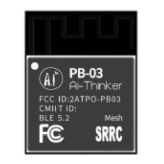
BLE-PB03 1. Product Overview PB-03 is a BLE module, the core processor chip PHY6252(SSOP24) of this module is a BLE SoC with high integration and low power consumption, which is specially designed for various applications such as IoT, mobile devices, wearable electronic devices and smart homes. -
Page 4: Characteristic
BLE-PB03 1.1. Characteristic Support BLE5.2, rate support:125Kbps, 500Kbps, 1Mbps, 2Mbps • Own 64 KB SRAM, 256KB flash, 96 KB ROM, 256bit efuse • Support UART/GPIO/ADC/PWM/I2C/SPI/PDM/DMA interface • Adopt SMD-52 package • Support multiple sleep modes, deep sleep current is less than 1uA •... -
Page 5: Static Electricity Requirements
BLE-PB03 2.1. Static electricity requirements PB-03 is an electrostatic sensitive device, and special precautions must be taken when handling it. Figure 2 ESD anti-static diagram 2.2. Electrical characteristics Table 2 Electrical characteristics table 2.3. BLE RF performance Table 3 BLE RF performance table... -
Page 6: Power Consumption
BLE-PB03 2.4. Power consumption The following power consumption data are based on a 3.3V power supply, ambient temperature of 25°C and measured using an internal regulator. All measurements were completed without the SAW filter at the antenna • interface. All emission data were measured based on the TX_Burst_Test&RX_Burst_Test •... -
Page 7: Appearance Dimensions
BLE-PB03 Appearance dimensions Figure 3 Appearance diagram pictures is for reference only, subject to physical objects) Figure 4 Module size diagram DS-BLE-PB03-1... -
Page 8: Pin Definition
BLE-PB03 4. Pin definition PB-03 has a total of 61 interfaces. As shown in below pin diagram, the pin function definition table is the interface definition. Figure 5 Schematic diagram of module pins (top view) DS-BLE-PB03-1... - Page 9 BLE-PB03 Table 6 Pin function definition table DS-BLE-PB03-1...
-
Page 10: Schematic
BLE-PB03 5. Schematic DS-BLE-PB03-1... -
Page 11: Antenna Parameters
BLE-PB03 6. Antenna parameters 6.1. Test conditions for the antenna Figure 7 Antenna test conditions DS-BLE-PB03-1... -
Page 12: Antenna S Parameter
BLE-PB03 6.2. Antenna S parameter Figure 8 Antenna S parameters 6.3. Antenna Gain and Efficiency Table 7 Antenna Gain and efficiency DS-BLE-PB03-1... -
Page 13: Antenna Field Type Diagram
BLE-PB03 6.4. Antenna field type diagram Figure 9 Antenna field type diagram DS-BLE-PB03-1... -
Page 14: Design Guidance
BLE-PB03 7. Design guidance 7.1. Module application circuit Figure 10 Application circuit diagram Note: Because the PB-03M does not have the reset pin, we can achieve the reduction by • power off, we can restore the module with a PMOS to achieve the reduction of power off. -
Page 15: Antenna Layout Requirements
BLE-PB03 7.2. Antenna layout requirements The installation position on the motherboard suggests the following 2 ways: • Scheme 1: Put the module on the edge of the motherboard, and the antenna area out of the motherboard edge. Scheme 2: Put the module on the edge of the motherboard, and empty an area along the antenna position. -
Page 16: Power Supply
BLE-PB03 7.3. Power supply Recommended 3.3V voltage, peak current over 200mA. • Power supply is recommend to use LDO; If the DC-DC is used, the ripple is • recommended to be controlled within 30mV. The DC-DC power supply circuit proposes to reserve the dynamic response •... -
Page 17: Gpio
BLE-PB03 7.4. GPIO Some IO ports are lead outside the module, if using, a proposed resistance of 10- • 100 ohms on the IO port. This suppresses the overshoot and enables smoother levels on both sides, helping for both EMI and ESD. -
Page 18: Flow Welding Curve Diagram
BLE-PB03 8. Flow welding curve diagram Figure 14 Flow welding diagram DS-BLE-PB03-1... -
Page 19: Product Related Models
BLE-PB03 9. Product related models Table 8 Product related model list DS-BLE-PB03-1... -
Page 20: Product Packaging Information
BLE-PB03 10.Product packaging information PB-03 module was packaged in a tape, 900pcs/reel. As shown in the below image: Figure 15 Package and packing diagram DS-BLE-PB03-1... - Page 21 RF Solutions Ltd shall not be liable for any loss or damage caused as a result of user’s own determination of how t o deploy or use R F Solu- tions Ltd’s products.
Need help?
Do you have a question about the BLE-PB03 and is the answer not in the manual?
Questions and answers