Table of Contents
Advertisement
e
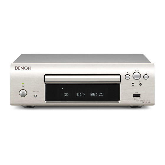
DCD-F109
• For purposes of improvement, specifications and design are subject to change without notice.
• Please use this service manual with referring to the operating instructions without fail.
• Some illustrations using in this service manual are slightly different from the actual set.
S0581-1V03DM/DG1211
SERVICE MANUAL
MODEL
COMPACT DISC PLAYER
Copyright 2012 D&M Holdings Inc. All rights reserved.
WARNING: Violators will be prosecuted to the maximum extent possible.
JP
E3
E2
P
e
D&M Holdings Inc.
Ver. 3
Please refer to the
MODIFICATION NOTICE.
E1
E1C
EA
E2R EUT
Advertisement
Table of Contents

Related Manuals for Denon DCD-F109


Summary of Contents for Denon DCD-F109
- Page 1 MODIFICATION NOTICE. SERVICE MANUAL MODEL E2R EUT DCD-F109 COMPACT DISC PLAYER • For purposes of improvement, specifications and design are subject to change without notice. • Please use this service manual with referring to the operating instructions without fail. • Some illustrations using in this service manual are slightly different from the actual set.
-
Page 2: Table Of Contents
CONTENTS ABOUT THIS MANUAL .............3 TROUBLE SHOOTING ............35 What you can do with this manual ..........3 FLOW CHART NO.1 ............35 Using Adobe Reader (Windows version) ........4 FLOW CHART NO.2 ............35 FLOW CHART NO.3 ............36 SAFETY PRECAUTIONS ............6 FLOW CHART NO.4 ............36 NOTE FOR SCHEMATIC DIAGRAM .........7 FLOW CHART NO.5 ............37 NOTE FOR PARTS LIST ............7... -
Page 3: About This Manual
ABOUT THIS MANUAL Read the following information before using the service manual. What you can do with this manual Search for a Ref. No. (phrase) Jump to the target of a schematic diagram (Ctrl+Shift+F) connector You can use the search function in Acrobat Reader to Click the Ref. -
Page 4: Using Adobe Reader (Windows Version)
Using Adobe Reader (Windows version) Add notes to this data (Sign) Magnify schematic / printed wiring board diagrams - 1 The Sign function lets you add notes to the data in this manual. (Ctrl+Space, mouse operation) Save the file once you have finished adding notes. Press Ctrl+Space on the keyboard and drag the mouse to select the area you want to view. - Page 5 Magnify schematic / printed wiring board Magnify schematic / printed wiring board diagrams - 2 diagrams - 3 (Pan & Zoom function) (Loupe Tool function) The Pan & Zoom function lets you see which part of a The Loupe Tool function lets you magnify a specific magnified diagram is being shown in a separate window.
-
Page 6: Safety Precautions
SAFETY PRECAUTIONS The following items should be checked for continued protection of the customer and the service technician. LEAKAGE CURRENT CHECK Before returning the set to the customer, be sure to carry out either (1) a leakage current check or (2) a line to chassis resistance check. -
Page 7: Note For Schematic Diagram
NOTE FOR SCHEMATIC DIAGRAM WARNING: Parts indicated by the z mark have critical characteristics. Use ONLY replacement parts recommended by the manufacturer. CAUTION: Before returning the set to the customer, be sure to carry out either (1) a leakage current check or (2) a line to chassis resistance check. If the leakage current exceeds 0.5 milliamps, or if the resistance from chassis to either side of the power cord is less than 460 kohms, the set is defective. - Page 8 WARNING AND LASER SAFETY INSTRUCTIONS WARNING WAARSCHUWING Alle IC’s en vele andere halfgeleiders zijn gevoelig All ICs and many other semi-conductors are voor elektrostatische ontladingen (ESD). susceptible to electrostatic discharges (ESD). Onzorgvuldig behandelen tijdens reparatie kan de Careless handling during repair can reduce life levensduur drastisch doen verminderen.
- Page 9 INSTRUCTIONS FOR HANDLING SEMI-CONDUCTORS AND OPTICAL UNIT Electrostatic breakdown of the semi-conductors or optical pickup may occur due to a potential difference caused by electrostatic charge during unpacking or repair work. 1. Ground for Human Body Be sure to wear a grounding band (1 MΩ) that is properly grounded to remove any static electricity that may be charged on the body.
-
Page 10: Technical Specifications
TECHNICAL SPECIFICATIONS n CD section n General • Digital output Power supply : AC 230 V, 50 Hz / 60 Hz Output Level (coaxial) : 0.5Vp-p, 75Ω Power consumption : 25 W Standby : 0.3 W DIMENSION 20.5 Ø30 Weight : 2.8kg... -
Page 11: Caution In Servicing
CAUTION IN SERVICING Initializing CD Player CD Player initialization should be performed when the μcom, peripheral parts of μcom, and CD PCB were replaced. Power operation switch (X) 1. Turn off the power pressing Power operation switch ( X ), unplug the power cord. 2. -
Page 12: Note Handling And Replacement Of The Laser Pick-Up
NOTE HANDLING AND REPLACEMENT OF THE LASER PICK-UP 1. Protection of the LD Short a part of the LD circuit by soldering. After connection to a circuit, remove the short solder. 2. Precautions when handling the laser CD mechanism • Handle the laser pick-up so that it is not exposed to dust. •... -
Page 13: Disassembly
DISASSEMBLY • Disassemble in order of the arrow in the following figure. • In the case of the re-assembling, assemble it in order of the reverse of the following flow. • In the case of the reassembling, observe "Caution concerning disassembly and assembly!". •... - Page 14 About the photos used for "descriptions of the DISASSEMBLY" section • The shooting direction of each photograph used herein is indicated on the left side of the respective photograph as "Shooting direction: ***". (*** : A,B,C,D) • Refer to the diagram below about the shooting direction of each photograph. •...
-
Page 15: Door
1. DOOR Proceeding : DOOR CABINET TOP → (1) You can slide in the arrow direction to pull out the TRAY. View from bottom (2) Detach the DOOR. PANEL LOADER... -
Page 16: Front Panel Assy
2. FRONT PANEL ASSY Proceeding : CABINET TOP DOOR FRONT PANEL ASSY → → (1) Remove the screws. View from the bottom (2) Cut the clamp bands, disconnect the connector wires and FFC Cable Remove the following, and then cut the clamp bands. (Not visible) Two screws on the left side of the transformer. -
Page 17: Cd Mechanism Assy
3. CD MECHANISM ASSY Proceeding : CABINET TOP DOOR FRONT PANEL ASSY → → CD MECHANISM ASSY → (1) Cut the clamp bands, disconnect the connector wires. Remove the screws. (2) Disconnect the connector wires. Connector wire Connector wire Shooting of photograph: C (3) Laser short-circuit in Pick-up of CD MECHANISM, then disconnect the FFC Cable. -
Page 18: Main Pcb
4. MAIN PCB Proceeding : CABINET TOP DOOR FRONT PANEL ASSY → → CD MECHANISM ASSY MAIN PCB → → Please refer to "EXPLODED VIEW" for the disassembly method of MAIN PCB. 5. POWER TRANS Proceeding : CABINET TOP POWER TRANS →... -
Page 19: Power Pcb
(2) Remove the screws. Shooting of photograph: A (3) Remove the screw. Shooting of photograph: C 7. POWER PCB Proceeding : CABINET TOP AUDIO PCB POWER PCB → → Please refer to "EXPLODED VIEW" for the disassembly method of POWER PCB. -
Page 20: Caution On Assembly
Caution on assembly (1) Caution about the ferrite core which attached to the power cord. Please check the following points. About 10mm so as not to contact, please clamp clearance. (2) Please make sure to clamp the cord and fixed it. Do not contacted the fuse or outlet even when it is pressed from above. -
Page 21: Special Mode
SPECIAL MODE Function summary 1. SERVICE MODE (1) Version No. of main μ-com Display mode (2) Version No. of USB μ-com Display mode (3) FLD check mode 2. CD TEST MODE (1) Disc loading (2) Servo check (3) Pickup movement (4) Stop (5) All servo on (6) Laser current is display... -
Page 22: Service Mode
1. SERVICE MODE (1) AC is turned on while pressing the 5 and 2 button same time on this unit.(Model name display) DCD-F109 1.1. Version No. of main μ-com Display mode (1) Press the 9 button. Ver xxxx (**** : Version number of main μ-com) 1.2. Version No. of USB μ-com Display mode (1) Press the 9 button while version No. - Page 23 2.2. Servo check (1) Press the 1 / 3 button. Execute the following steps. • 13 flashing q LD ON (with servo still stopped) LD ON w FOCUS ON (disc rotation, tracking off) If no disc loaded, retry then stop. Focus ON e CLV ON CLV ON...
- Page 24 2.3. Pickup movement (1) In the stop mode, pickup moves in REV (inwards) or FWD (outwards) direction when 8 or 9 button pressed. (2) When 8 button pressed, move to stop operation after detection that inner switch has turned on. (3) Pickup movement stops when button released.
- Page 25 2.7. Adjustment value display (1) Press the 2 button after executing the servo auto adjustment (2.5). (2) When 9 button is pressed, the adjustment values are displayed in the following order. • 13 flashing q FOCUS BALANCE FOCUS BALANCE (XX : Adjustment value) w FOCUS GAIN FOCUS GAIN (XX : Adjustment value)
- Page 26 2.8. Accumulated laser on time display (1) When the DISC/USB and 5 button is pressed while the this unit is in the stop mode (CD TEST MODE display), the accumulated laser on time is displayed. (2) The laser drive times are added and the result is displayed. (3) One count corresponds to 10 minutes.
-
Page 27: Cd Heat Run Mode
3. CD HEAT RUN MODE (1) AC is turned on. (2) Press the 5 button to open the tray. (3)Set a disc on the tray, then press the 5 button again to close the tray. (4) AC is turned off. (5) AC is turned on while pressing the 5 and 2 button same time on this unit. - Page 28 3.2. Heat run Short mode (1) Press the 1 / 3 button while name of the H.R.SHORT is displayed. H.R.SHORT (2) Count this as the 0th heat run repetition. q Play the last track only on disc. Normal display except when 1 light, 3 light. w After disc playback has finished, move pickup to innermost position and open tray.
- Page 29 3.3. Heatrun checking mode • Normal display except when 1 flashing, 3 flashing. (1) Press the 1 / 3 button while name of the H.R.CHACKING is displayed.. H.R.CHACKING (2) Count this as the 0th heat run repetition q Play the last track only on disc. XXXX (XXXX : No.
-
Page 30: Cold Start (Initialize)
q Number of heat run is display (1) Press the 9 button while the error is displayed. (2) No. heat runs is displayed for 5 seconds, the error display reappears. XXXX (XXXX : No. of heat run repetitions) w The track no. and time when the error occurred is displayed. (1) Press the 8 button while the error is displayed. -
Page 31: Special Mode Transition Diagram
Special mode transition diagram... - Page 32 Personal notes:...
-
Page 33: When The Microprocessor Is Replaced With A New One
WHEN THE MICROPROCESSOR IS REPLACED WITH A NEW ONE When the U-PRO (Microprocessor) or the Flash ROM is replaced, confirm the following. After PWB Name Ref. No. Description Remark replaced MAIN IC11 TMP92FD23AFG IC15 TMP92FD28AFG After replacing A : Mask ROM (With software). No need for write-in of software to the microprocessor. B : Flash ROM (With software). - Page 34 t When a file is not found SYSTEM VUP FileError (5) After Version UP is completed, a tray is opened and it stops in SYSTEM VUP Complete 1.2.2. USB μ-com (1) AC is turned on while pressing the 5 and 2 button same time on this unit.(Entering the Service mode) (2) While displaying model name, when 9 and the POWER button are pressed simultaneously, the tray opens.
-
Page 35: Trouble Shooting
TROUBLE SHOOTING FLOW CHART NO.1 The power cannot be turned on. Is Power LED lit? Check if there is any leak or short-circuiting rectifier circuit of SUB Power transformer, and service it if defective. (PT601,IC611,Q609-Q612,D633-D638) Is the +3.3V_NSW line voltage normal? Is the "H"... -
Page 36: Flow Chart No.3
FLOW CHART NO.3 The fluorescent display tube does not light up. Is +3.3V_D voltage supplied to Pins(37) of FLT500? Check the +3.3V_D line and service it if defective. Is the voltage of approximately +42V supplied to Pin(38) of FLT500? Check D619,D620,ZD605,ZD606,Q608 and the periphery circuit, and service it if defective. -
Page 37: Flow Chart No.5
FLOW CHART NO.5 No operation is possible from the remote control unit. Are the System Remote Connector Cables normal? Check IC608 and the periphery circuit, and service it if Is +5V voltage supplied to Pin(14) of IC606,IC607? defective. Refer to DRA-F109 TROUBLESHOOTING_Remote Are the Control Signals of JACK602,JACK603 normal? Control Check IC606,IC11 and the periphery circuit, and service it if defective. -
Page 38: Flow Chart No.8
FLOW CHART NO.8 USB PLAY don't work normally. Check the voltage of +3.3V is supplied to Pin(3) of IC21. Check the voltage of +3.3V is supplied to Pin(4) of IC21. Is VBUS(+5V) voltage supplied to Pin(1) of JACK500? Check the voltage of +5V_D is supplied to Pin(6) of IC21. Check the voltage of +5.0V is supplied to Pin(3) of IC605. -
Page 39: Measuring Method And Waveforms
MEASURING METHOD AND WAVEFORMS MEASURING POINT MAIN CD UNIT (Component side) ① RFEQO ② RFO BN81 C538 C536 C534 C541 C542 C535 C537 C533 C202 C211 R268 ⑨OPSW R606 R255 R605 CN21 R604 R715 R259 R238 R714 R713 R198 R712 R264 R241 R811 R243 R185... - Page 40 CUP12471Z CD ASSY (Foil side) ⑤TEI ③FSMONIT (IC17 : 24pin) (IC17 : 21pin) C238 C235 C239 L203 C240 C555 C236 C237 C282 C281 IC20 IL1117H-1.5 C532 C556 C288 C287 C214 C206 C215 L202 C292 R130 C227 C205 C226 R202 R133 R813 R814 C217...
-
Page 41: Waveforms
WAVEFORMS 1. DISC PLAY RF WAVEFORM(EYE-PATTERN) 2. DISC DETECTION 1.1 CD(TCD-784)Play 2.1 CD(TCD-784)DISC DETECTION ②RFO 200mV ③FSMONIT ④FOO ①RFEQO 500Mv ⑤TEI ⑥ TRO ⑦FMO ⑧DMO 2.2 CD-R(TCD-R000RM)DISC DETECT 1.2 CD-R(TCD-R000RM)Play ②RFO 200mV ③FSMONIT ④FOO ①RFEQO 500Mv ⑤TEI ⑥ TRO ⑦FMO ⑧DMO 1.3 CD-RW(TCD-W000RM)Play 2.3 CD-RW(TCD-W000RM)DISC DETECTION... - Page 42 3. TOC READ 4. FOCUS ADJUSTMENT 3.1 CD(TCD-784)TOC READ 4.1 CD(TCD-784)FOCUS ADJUSTMENT ②RFO ③FSMONIT 200mV ④FOO ⑤TEI 500Mv ⑥ TRO ⑦FMO ⑧DMO 3.2 CD-R(TCD-R000RM) (TCD-R000RM)FOCUS ADJUSTMENT ②RFO ③FSMONIT 200mV ④FOO ⑤TEI 500Mv ⑥ TRO ⑦FMO ⑧DMO 3.3 CD-RW(TCD-W000RM)TOC READ 4.3 CD-R(TCD-R000RM)FOCUS ADJUSTMENT ②RFO 1V...
-
Page 43: Block Diagram
BLOCK DIAGRAM RESET IC (ON SEMI) GATE NCP300 SPI EEPROM 4k (ST) REMOTE CONNECTOR 1 M95010W OPEN / CLOSE REMOTE CONNECTOR 2 OPEN_SW / CLOSE_SW SPIN +/- SLED +/- SYSTEM CD RST TR +/- FC +/- MOTOR IN/OUT F +/- TR +/- DRIVER CD DSP... -
Page 44: Wiring Diagram
WIRING DIAGRAM DC-DC_PCB AC_CORD 8P_WAFER 7P_WAFER FROM AUDIO_PCB FROM POWER_PCB 8P_WIRE TO DC-DC_PCB AC_OUTLET 3P_WIRE TO MAIN_PCB 2P_WAFER AUDIO_PCB BD_TO_BD 15P FROM AC_CORD TO POWER_PCB POWER_PCB 3P_WAFER FROM TRANS 7P_WIRE BD_TO_BD 15P TO DC-DC_PCB 7P_WAFER 5P_WAFER FROM AUDIO_PCB FROM FRONT_PCB FROM TRANS 2P_WAFER 11P_WIRE... -
Page 45: Printed Wiring Boards
PRINTED WIRING BOARDS MAIN CD UNIT MAIN CD UNIT (COMPONENT SIDE) (FOIL SIDE) C619 C235 C238 C621 C239 C620 L203 C240 C555 C236 C237 C282 C281 IC20 BN81 IL1117H-1.5 C532 C556 C538 C536 C534 C541 C542 C558 C288 C537 C535 C533 C214 C287... - Page 46 POWER FRONT (COMPONENT SIDE) (COMPONENT SIDE) ZD606 MTZ33B C784 ZD605 MTZ9.1B C783 JACK604 J641 ANALOG OUT BONDING JACK601 T601 DIGITAL OUT J505 J504 C719 3300/16V S504 S500 J620 JACK605 IC613 S505 C726 NJM7808FA J654 S502 S501 ZD604 CLP600 LED500 MTZ3.6B F601 J602 CP604...
- Page 47 POWER DC-DC Converter (COMPONENT SIDE) (COMPONENT SIDE) J609 C641 R652 J610 C697 C690 CP605 C655 C674 J663 R688 J624 C679 R672 R650 R670 R689 R690 J607 J627 C640 J608 J605 J606 DCD-F109_AUDIO C603 C633 CN610 BKT1 TO DC/C BD 7020-07196-000-0S POWER (FOIL SIDE) DC-DC Converter...
-
Page 48: Schematic Diagrams (1/5)
RESET IC 3V VERSION SEL CD DSP PARTS MCU UNIT C120 4700N-K-1608 C121 42PIN 43PIN MODE R243 R242 10K-1608 C122 HOST MCU PARTS R234 10K-1608 CD DSP IC12 NCP300LSN30T1 TC94A92FG R226 0-1608 R162 R225 100-1608 R224 100-1608 10K-1608 HOST MCU R223 100-1608 R291... -
Page 49: Sub Power Unit
SUB POWER UNIT JACK602 H/P-JACK(D3.5-SW) DENON BUS 1 R687 R667 L602 BD121T R691 (OUT) R683 R668 L603 BD121T R692 R669 C678 22/6.3-Z8154 C679 100N-K C680 10N-K R672 C687 100N-K C688 1N-K C689 10N-K TO CN610 D606 KDS160 D607 KDS160 C690... -
Page 50: Audio Part
100N-K GND_D C636 1N(EB)-100V C640 C638 100N-K GND_D R641 R642 R643 R644 C639 DENON BUS INT 100/50(ELNA) IC604:A NJM2068MD DENON BUS TXD C775 100N-K DENON BUS RXD DENON BUS SW2 C776 100N-K DENON BUS SW1 DENON BUS CONT2 DENON BUS CONT1... -
Page 51: Power Part
IC615 C783 TC7SH04F 33/16 CN602 CN602 R665 R664 SPDIF COAXIAL OUT GND_D GND_D L601 BD121T 100N-K C672 C677 10N-K CP604 CP604 10N-K C674 C125Z1-11 C694 C695 100N-K C673 100N-K 10N-K GND_D2 GND_D2 C692 C675 10N-K C693 +3.3V_CPU 100N-K 10N-K +3.3V_CPU +3.3V_D2 +3.3V_D2 C707... -
Page 52: Dcdf109 Display Unit
DCDF109 DISPLAY UNIT DISPLAY PARTS KEY PARTS R500 R501 R502 R503 R504 TONE TUNED AUTO ST MONO RANDOM TOTAL 1 FLD ALL SLEEP C500 100N-K R505 R506 R507 4 5 6 32 33 R508 R509 R510 R511 C501 100N-K C502 R512 CP501 CP501... -
Page 53: Exploded View
EXPLODED VIEW WARNING: Parts marked with this symbol have critical characteristics. Use ONLY replacement parts recommended by the manufacturer. 印の部分は安全を維持するために重要 な部品です。従って交換時は必ず指定の 部品を使用してください。... -
Page 54: Exploded View Of Cd Mechanism Unit
EXPLODED VIEW OF CD MECHANISM UNIT WARNING: Parts marked with this symbol have critical characteristics. Use ONLY replacement parts recommended by the manufacturer. 印の部分は安全を維持するために重要 な部品です。従って交換時は必ず指定の 部品を使用してください。... -
Page 55: Parts List Of Exploded View
PARTS LIST OF EXPLODED VIEW z Parts indicated by "nsp" on this table cannot be supplied. z P.W.B. ASS'Y indicated by "nsp" on this table cannot be supplied. When repairing the P.W.B. ASS'Y, check the board parts list and order replacement parts. -
Page 56: Parts List Of Cd Mechanism Unit
Ref. No. Part No. Part Name Remarks Q'ty New ★ 32 BRACKET,PCB A 4010215586000S ★ 33 BRACKET,CD MECHA 4010215666000S ★ 34 CLAMP CABLE 4330040343010S ★ 35 963611500600S CORD ASSY,2.5A/250V EU L068250250611S ★ 35 963611500610S CORD ASSY,7A/125V L068125070010S 963471100650S CUSHION RUBBER SPONGE 14*5*4.5t 4050214495000S SCREWS "SCREW... -
Page 57: Packing View
PACKING VIEW... -
Page 58: Parts List Of Packing & Accessories
PARTS LIST OF PACKING & ACCESSORIES z Parts indicated by "nsp" on this table cannot be supplied. z Parts indicated by the " ★ " mark are not illustrated in the exploded view. z The parts listed below are only for maintenance. Therefore they might differ from the parts used in the unit in appearances or dimensions. Note: The symbols in the column "Remarks"... -
Page 59: Semiconductors
(Schmitt I input) (data) PF1/RXD0 OPEN Non (NC) (Schmitt I input) PF2/SCLK0/CTS0/ FL tube communication line FL_CLK (Schmitt I input) (clock) DENON BUS PF3/TXD1/HSSO [TXD] [Communication lines for (Schmitt I input) writing] DENON BUS PF4/RXD1/HSSI [RXD] [Communication lines for (Schmitt I input) - Page 60 (Schmitt I input)§When resetting PN3/SCK1 E2P_CLK for E2PROM it, it becomes output latch 1. PD0/TB0OUT0/ /DB RXB (INT) DENON BUS (Schmitt I input) INT4 " P o w e r s u p p l y DVSS Power supply (GND) (GND)"...
- Page 61 IC Terminal name Terminal name Terminal function Remarks Setting P47/A7 DAC_MDI DAC1796 MDI P5x : Setting is possible by 1bit P50/A8 DAC_MCK DAC1796 MCK unit P51/A9 DXP_CS Chip selector for DXP6000 P52/A10 DXP_RST Reset for DXP6000 P53/A11 BU_CS Chip selector for BU2630 P54/A12 MCK_SEL MCLK selector...
- Page 62 IC Terminal name Terminal name Terminal function Remarks Setting DVSS Power supply(GND) Power supply (GND) PL3/AN11/ADTRG DBUS_SW1 Port only for input (Schmitt ) PL2/AN10 DBUS_SW2 Port only for input (Schmitt ) PL1/AN9 USB_FLAG IC21 NCP380(4) /FLAG Port only for input (Schmitt ) PL0/AN8 100KΩ/PD Port only for input (Schmitt )
- Page 63 TMP92CD28AFG (IC15) TMP92CD28AFG (IC15) DCD-710AE...
- Page 64 TMP92CD28AFG Block Diagram TMP92CD28AFG Block Diagram TMP92CD28AFG Terminal Function DCD-710AE/755SE Pull IC Terminal name RST INIT Port function Terminal name /RESET RESETTerminal Port only for input (Schmitt input and PU resistance) PC0/INT0 Reserved Port only for input (with Schmidt input) PC1/INT1 Non (PD) Port only for input (with Schmidt input)
- Page 65 TMP92CD28AFG Terminal Function Port Name Note Init STB. Pull U/D /RESET RESET PU/PD PC0/INT0 INT0 PC1/INT1 Not used(PD) PC2/INT2/TB1IN0/TB0IN0 Not used(PD) PC3/INT3 STREQ DVCC3B Vcc(+3.3V) Sub-CLK(NC) Sub-CLK(NC) Output control(NC) DVSS VSS(GND) DVCC1B VCC(+1.5V) RVOUT1 Internal +1.5V Regulator output RVIN Internal +1.5V Regulator output RVIN Internal +1.5V Regulator output RVOUT2...
- Page 66 Port Name Note Init STB. Pull U/D P55/A13 CONT1(Reserved for system u-com) P56/A14 CONT2(Reserved for system u-com) O(L) P57/A15 CONT3(Reserved for system u-com) P60/A16 Not used(NC) O(L) P61/A17 Not used(PD) O(L) P62/A18 P63/A19 BUCK P64/A20 BUS0 P65/A21 BUS1 P66/A22 BUS2 P67/A23 BUS3 DVSS...
- Page 67 TC94A92FG (IC17) TC94A92FG (IC17) DCD-710AE...
- Page 68 TC94A92FG Terminal Function TC94A92FG Terminal Function Default Symbol Description Remarks DSP VCO - EFM and PLCK Phase difference VCoi signal output pin. 3 state output 3AI/F (DSP VCO control voltage inputr pin.) CD-DSP-Power supply for 3.3V RF RVDD3 amplifier core and PLL circuit Connect capacitor according with se SLCo EFM slice level output pin...
- Page 69 Default Symbol Description Remarks Focus Error signal / Sub beam add signal FSMoNiT 3AI/F output pin(monitor pin/GND) RFZi 3AI/F RFRP 3AI/F Bulit-in serises R=500 Connect to VRo by 3AI/F capacitor. AVDD3 Power supply pin for 3.3 V CD analog circuits. Bulit-in serises R=3.3 k 3AI/F Bulit-in output R=3.3 k...
- Page 70 Symbol Description Default Remarks DVSS3R Grounding pin for 3.3V Muiti-Bit DAC circuit R channel audio output pin of Audio DAC. 3AI/F DVDD3R Power supply pin for 3.3V Audio DAC circuit. DVDD3L Power supply pin for 3.3V Audio DAC circuit. L channel audio output pin of Audio DAC 3AI/F DVSS3L Grounding pin for 3.3V Muiti-Bit DAC Circuit...
- Page 71 Symbol Description Default Remarks VDD3 Power Supply pin for 3.3V Digital circuit CMOS Port Schmitt input BUS0 Microprocessor I/F data input/output pin 0 3I/F Refer to [1.2 Pin Assinment Table] CMOS Port Schmitt input BUS1 Microprocessor I/F data input/output pin 1 3I/F Refer to [1.2 Pin Assinment Table] CMOS Port...
- Page 72 IP4001 (IC14)CR Pin Discriptions The IP4001CR is a monolithic integrated circuit, and suitable for 5ch motor driver which drives focus ...
- Page 73 Operation temperature –25 °C θ JA Thermal resistance 28-pin SSOP °C/W (1) Input is BPZ data. PIN ASSIGNMENTS PCM1796DBR (IC602) PCM1796 (TOP VIEW) ZEROL ZEROR AGND3L MSEL L– LRCK DATA AGND2 DGND AGND1 R– AGND3R PCM1796 www.ti.com SLES100A − DECEMBER 2003 − REVISED NOVEMBER 2006 PCM1796DBR Block Diagram FUNCTIONAL BLOCK DIAGRAM I OUT L–...
- Page 74 PCM1796 www.ti.com SLES100A − DECEMBER 2003 − REVISED NOVEMBER 2006 Terminal Functions PCM1796DBR Pin Discriptions TERMINAL DESCRIPTIONS DESCRIPTIONS NAME AGND1 – Analog ground (internal bias) AGND2 – Analog ground (internal bias) AGND3L – Analog ground (L-channel DACFF) AGND3R – Analog ground (R-channel DACFF) Bit clock input (1) Serial audio data input (1) DATA...
-
Page 75: Fl Display
2. FL DISPLAY V.F.D (16-ST-103GINK) (FLT500) PIN CONNECTION GRID ASSIGNMENT... - Page 76 GRID ASSIGNMENT...
-
Page 78: Parts List Of P.c.b. Unit
PARTS LIST OF P.C.B. UNIT z Parts indicated by "nsp" on this table cannot be supplied. z The parts listed below are only for maintenance. Therefore they might differ from the parts used in the unit in appearances or dimensions. Note: The symbols in the column "Remarks"... - Page 79 Ref. No. Part No. Part Name Remarks Q'ty C217 C,CERAMIC 0.047UF-K/16V D011473773160S C219 C,CERAMIC 0.047UF-K/16V D011473773160S C220-222 C,CERAMIC 0.1UF-K/50V D011104577160S C223 C,CERAMIC 0.01UF-K/50V D010103777160S C224 C,CERAMIC COG47PF-J/50V D010470167160S C225 C,CERAMIC X7R0.015UF-K/50V D011153777160S C226 C,CERAMIC 0.01UF-K/50V D010103777160S C227 C,CERAMIC 470PF-J/50V D010471167160S C231 C,CERAMIC 1000PF-K/50V D011102777160S...
- Page 80 Ref. No. Part No. Part Name Remarks Q'ty C671 C,CERAMIC CHIP 6800PF-K/50V-1608REEL D011682777160S C672 C,CERAMIC 0.1UF-K/50V D011104577160S C673-675 C,CERAMIC 0.01UF-K/50V D010103777160S C678 C,ELECT CHIP 22UF-MV/6.3V D050220081460S C679 C,CERAMIC 0.1UF-K/50V D011104577160S C680 C,CERAMIC 0.01UF-K/50V D010103777160S C685 C,CERAMIC 0.1UF-K/50V D011104577160S C686 C,CERAMIC 1000PF-K/50V D011102777160S C687 C,CERAMIC 0.1UF-K/50V...
-
Page 81: Front P.w.b. Unit Ass'y
FRONT P.W.B. UNIT ASS'Y Ref. No. Part No. Part Name Remarks Q'ty New SEMICONDUCTORS GROUP IC601 00D2630896909 IC,LINEAR OP,NJM2068MD-SOP8P J121206800030S IC602 00D2623362903 IC,LOGIC-D/A CONVER,PCM1796DBR J042179600010S IC603,604 00D2630896909 IC,LINEAR OP,NJM2068MD-SOP8P J121206800030S IC609 963231101220S IC,LINEAR-REGULATOR,KIA1117BPI33 J126111733110S IC610 00D2630810008 IC NJM7808FA J126780800030S IC611 00D2622977946 IC,LINEAR-REGULATOR,BA33BC0FP J12603R300040S... - Page 82 Ref. No. Part No. Part Name Remarks Q'ty New C521 C,CERAMIC 0.1UF-K/50V D011104577160S C522 C,ELECT 220UF-M/6.3V D040221081070S C523,524 C,CERAMIC 0.1UF-K/50V D011104577160S C525 C,CERAMIC 0.01UF-K/50V D010103777160S C526 C,CERAMIC 1000PF-K/50V D011102777160S C527 C,CERAMIC 0.1UF-K/50V D011104577160S C528 C,CERAMIC 0.01UF-K/50V D010103777160S C601 00D9630216304 C,FILM 0.001UF-J/100V D02010206C060S C603,604 00D2544693939...
- Page 83 Ref. No. Part No. Part Name Remarks Q'ty New C723 C,CERAMIC 0.1UF-K/50V D011104577160S C724 CER. CAP. X5R)0.33UF-Z/25V-1608REEL D011334794160S C725 C,CERAMIC 0.1UF-K/50V D011104577160S C726 00D9639005804 C,ELECT 100UF-M/25V D040101084060S C727 00D9630217002 C,ELECT 3300UF-M/16V D040332083010S C728 C,CERAMIC 0.1UF-K/50V D011104577160S C729 CER. CAP. X5R)0.33UF-Z/25V-1608REEL D011334794160S C730 C,CERAMIC 0.1UF-K/50V...
- Page 84 Ref. No. Part No. Part Name Remarks Q'ty New CP501 CN.FPC 15P L130100111510S CP601 CN.WAFER 5P 5267-05A L102526700500S CP602 CN.WAFER 7.92MM,PLUG YW396-03AV 2P L108396030010S CP603 CN.WAFER 3P 5267-03A L102526700300S CP604 CN,WAFER C125Z1-15 15P L109012511520S CP605 CN,WAFER 15P C125Z2-15 L109012521510S CP605 CN,WAFER C125Z2-15 L109012521520S CP606...
Need help?
Do you have a question about the DCD-F109 and is the answer not in the manual?
Questions and answers