Denon DCD-F101 Service Manual
Stereo cd player
Hide thumbs
Also See for DCD-F101:
- Specifications (2 pages) ,
- Operating instructions manual (52 pages) ,
- Operating instruction (89 pages)
Advertisement
Table of Contents
- 1 Laser Radiation
- 2 Front Panel
- 3 CD Test Mode
- 4 Wave-Forms of each Point
- 5 Block Diagram
- 6 Power Unit
- 7 Main Unit
- 8 Display Unit
- 9 Pin Connection
- 10 Note for Parts List
- 11 Parts List of P.w.b. Unit
- 12 Parts List of Exploded View
- 13 Exploded View of CD Mechanism Unit (Cd11Fta3N)
- 14 Parts List of CD Mechanism Unit
- 15 Packing View
- 16 Parts List of Packing & Accessories
- Download this manual
See also:
Operating Instructions
MODEL
●
For purposes of improvement, specifications and
design are subject to change without notice.
●
Please use this service manual with referring to
the operating instructions without fail.
●
Some illustrations using in this service manual are
slightly different from the actual set.
SERVICE MANUAL
DCD-F101
STEREO CD PLAYER
注 意
サービスをおこなう前に、このサービスマニュアルを
必ずお読みください。本機は、火災、感電、けがなど
に対する安全性を確保するために、さまざまな配慮を
おこなっており、また法的には「電気用品安全法」に
もとづき、所定の許可を得て製造されております。
従ってサービスをおこなう際は、これらの安全性が維
持されるよう、このサービスマニュアルに記載されて
いる注意事項を必ずお守りください。
TOKYO, JAPAN
Denon Brand Company, D&M Holdings Inc.
● 本機の仕様は性能改良のため、予告なく変更すること
があります。
● 補修用性能部品の保有期間は、製造打切後 8年です。
●
修理の際は、必ず取扱説明書を参照の上、作業を行って
ください。
● 本文中に使用しているイラストは、説明の都合上現物
と多少異なる場合があります。
For Europe model
Ver. 2
Please refer to the
MODIFICATION NOTICE.
,
X 0149V.02 DE/CDM 0603
Advertisement
Table of Contents

Related Manuals for Denon DCD-F101


Summary of Contents for Denon DCD-F101
- Page 1 Please use this service manual with referring to the operating instructions without fail. ください。 ● 本文中に使用しているイラストは、説明の都合上現物 ● Some illustrations using in this service manual are slightly different from the actual set. と多少異なる場合があります。 TOKYO, JAPAN Denon Brand Company, D&M Holdings Inc. X 0149V.02 DE/CDM 0603...
-
Page 2: Laser Radiation
DCD-F101 SAFETY PRECAUTIONS The following check should be performed for the continued protection of the customer and service technician. LEAKAGE CURRENT CHECK Before returning the unit to the customer, make sure you make either (1) a leakage current check or (2) a line to chassis resistance check. -
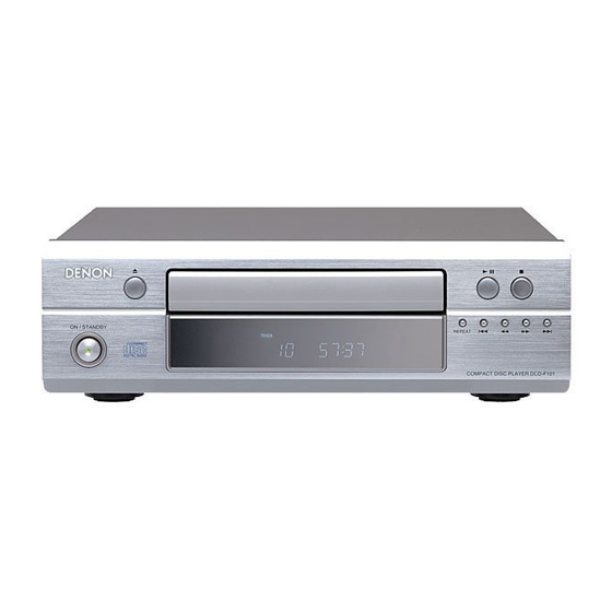
Page 3: Front Panel
DCD-F101 DISASSEMBLY (Follow the procedure below in reverse order when reassembling.) 1. Top Cover Top Cover 1) Remove 2 screws on both sides. 2) Remove 5 screws and detach the Top Cover as shown in the arrow dire ction. 2. Front Panel 1) Move the lever of the CD Mecha. - Page 4 DCD-F101 3. Display P.W.B. 1) Remove 8 screws and detach the Display P.W.B. Display P.W.B. 4. Power P.W.B. 1) Remove 2 screws and 1 screw 2) Lift the Power P.W.B., and disconnect a connector (connected with the µ-com P.W.B.). 3) Disconnect a connector (connected with the trans).
- Page 5 DCD-F101 5. CD Mecha. Unit 1) Open the Tray completely by turning the gear under the Mecha. Unit counterclockwise. 2) Remove 2 screws on the Tray. 3) Remove 2 rear screws fixing the CD Mecha. 4) Detach the CD Mecha. in the arrow direction.
-
Page 6: Cd Test Mode
DCD-F101 CD TEST MODE Setting of the test mode How to start the test mode: Turn on the power in the condition that CLSW (Test Point) and OPSW (Test Point ) are being shorted. ( “01” is indicated on the DISPLAY) To exit from the test mode, turn off the power. - Page 7 DCD-F101 How to check the test mode ( 1 ) DISC discrimination, adjustment * Insert DISC, and press the AUTO SEARCH REVERSE button. * “06 Adj” is displayed, and discrimination of DISC size 8 cm/12 cm, discrimination of DISC reflectance (CD, CD- R/CD-RW), adjustment of focus, tracking offset, and EF balance will be performed.
-
Page 8: Wave-Forms Of Each Point
DCD-F101 WAVE-FORMS OF EACH POINT When 12 cm DISC When 12 cm DISC stop start When 8 cm DISC When 8 cm DISC stop start During PAUSE When focus servo on Track search Track search (when forward) (when reverse) During PLAY... -
Page 9: Block Diagram
DCD-F101 BLOCK DIAGRAM OPT.OUT CD/RW PICK RW SW LD ON L.DIODE FOCUS MUTE FOCUS COIL Drv. COIL LA9241M LC78625E TRACKING TRACKING AC Cord OUTLET IC101 IC102 COIL COIL Drv. SLIDE MAIN Mtr. Drv. TRANS SLIDE DF & DAC PCM1735 SPINDLE... - Page 10 DCD-F101 SEMICONDUCTORS IC’s µ µ µ µ µ PD78044FGF (IC603) 64 63 62 61 60 59 58 57 56 55 54 53 52 51 50 49 48 47 46 45 44 43 42 41 P113/FIP21 P33/TI1 P112/FIP20 P34/TI1 P111/FIP19 P35/PCL...
- Page 11 Model discri. input terminal (H: Domestic, L: Overseas) INPT2 For DSP control INPT1 Disc reflection check INPT0 SCIDIN DENON bus interrupt monitor input terminal VSS Internal connection, connect to Vss directly FSEQ Serve status check input terminal...
- Page 12 DCD-F101 LC78625E (IC102) SQOUT AS DEPC /P2 CO IN AS DFIN/P1 CQCK AS DACK /P0 TS T10 TST11 DAC KO LASER DFOLO DFORO 4.2M LRCKO CONT EMPH TEST5 TE ST4 DEMO XOUT TE ST3 TEST1 THLD 9 10 11 12 13 14 15 16 17 18 19 20 21 22 23 24 RAM address 2k ´...
- Page 13 DCD-F101 LA6559 (IC103) Function Name Thermal 5CH output change terminal, logic input of Shutdown loading block Signal System VCC Signal System GND signal system power supply S-VCC S-GND S-Vcc Input Power Supply (BTL-AMP:CH1~4) (Forward/Reverse/ (LOADING) CH2 to CH4 VCC2 MUTE2...
- Page 14 DCD-F101 PCM1735E Terminal Function PCM1735E (IC301) Function Name LRCK LRCK clock input (fs) LRCK ML/IIS DATA Data input DATA MC/DM1 Bit clock input for data MD/DM0 CLKO System clock, buffer output CLKO MUTE X'tal oscillator connect or ext. clock input...
- Page 15 DCD-F101 TRANSISTORS 2SA1037K 2SC2412K 2SC3326(A/B) DTA144EK DTA Series DTC Series DTA124XK DTC114EK DTC124EK DTC144EK DTC144TK DTC114EK 10kohm /W 10kohm /W DTA144EK 47kohm /W 47kohm /W VIEW DTA124XK 22kohm /W 47kohm /W DTC124EK 22kohm /W 22kohm /W DTC144EK 47kohm /W 47kohm /W...
-
Page 16: Pin Connection
DCD-F101 FL DISPLAY 11-BT-199GNK (FL701) GRID ASSIGNMENT [11G~2G] PIN CONNECTION PIN NO. CONNECTION NOTE 1) F1,F2 ---- Filament 2) NP -------- No pin 3) NX -------- No extend pin 4) NC -------- No connection (NC pin should be electrically open on the PC board) - Page 17 DCD-F101 PRINTED WIRING BOARDS 1U-3455 CD P .W.B. UNIT COMPONENT SIDE...
- Page 18 DCD-F101 1U-3455 CD P .W.B. UNIT FOIL SIDE...
-
Page 19: Note For Parts List
DCD-F101 NOTE FOR PARTS LIST Part indicated with the mark " " are not always in stock and possibly to take a long period of time for supplying, or in some case supplying of part may be refused. When ordering of part, clearly indicate "1" and "I" (i) to avoid mis-supplying. -
Page 20: Parts List Of P.w.b. Unit
DCD-F101 PARTS LIST OF P.W.B. UNIT 1U-3455 CD P.W.B. ASS'Y Ref. No. Part No. Part Name Remarks Ref. No. Part No. Part Name Remarks SEMICONDUCTORS GROUP LD701 393 9618 007 Double Color LED SLR-9336DS-91 IC101 263 1090 005 IC LA9241M... - Page 21 DCD-F101 Ref. No. Part No. Part Name Remarks Ref. No. Part No. Part Name Remarks R160 247 2008 926 RM73B--222JT R507,508 247 2011 942 RM73B--473JT R161 247 2010 985 RM73B--273JT R509 247 2018 903 RM73B--0R0KT R162 247 2010 998 RM73B--303JT...
- Page 22 DCD-F101 Ref. No. Part No. Part Name Remarks Ref. No. Part No. Part Name Remarks CAPACITORS GROUP C176 257 0501 901 CK73B1H103KT (1608) C177 254 4524 972 CE04W1H4R7MT SMG/RE3 C101 257 0512 903 CK73F1E104ZT C178 257 0517 908 CK73B1C473KT C104-109...
- Page 23 DCD-F101 Ref. No. Part No. Part Name Remarks Ref. No. Part No. Part Name Remarks Q'ty C601 257 0512 903 CK73F1E104ZT JK301 204 8639 004 2P PIN JACK (C-GND) C602 254 4538 900 CE04W1C100MT SMG/RE3 JK401,402 204 8637 006 MINI JACK (STEREO)
- Page 24 DCD-F101 EXPLODED VIEW WARNING: Parts marked with this symbol have critical characteristics. Use ONLY replacement parts recommended by the manufacturer.
-
Page 25: Parts List Of Exploded View
18 412 4967 009 PWB BRACKET(CD) 19 415 0890 001 INSULATING SHEET 20 144 2803 204 FRONT PANEL 21 131 0156 106 DENON BADGE 22 146 2286 209 INNER PANEL(CD&DR) 23 143 1151 006 WINDOW 24 113 1934 002 KNOB 2P ASS’Y 25 113 1936 000 KNOB 5P ASS’Y... -
Page 26: Exploded View Of Cd Mechanism Unit (Cd11Fta3N)
DCD-F101 EXPLODED VIEW OF CD MECHANISM UNIT (CD11FTA3N) PARTS LIST OF CD MECHANISM UNIT Ref. No. Part No. Part Name Remarks Q'ty Ref. No. Part No. Part Name Remarks Q'ty 1 964 0009 006 Frame chassis 11 964 0010 008 Mecha lifter... -
Page 27: Packing View
DCD-F101 PACKING VIEW PARTS LIST OF PACKING & ACCESSORIES Ref. No. Part No. Part Name Remarks Q'ty Ref. No. Part No. Part Name Remarks Q'ty 201 505 0038 030 POLY COVER 207 502 1065 003 CUSHION (L) 202 511 3915 003 INST.MANUAL(E2) 208 502 1066 002 CUSHION (R) 203 515 0921 005 S.S.LIST(EX) - Page 28 DCD-F101 SCHEMATIC DIAGRAMS (1/2) 2.74 5V (Unswitched) 5V (Switched) SIGNAL LINE NOTICE WARNING: ALL RESISTANCE VALUES IN OHM. k=1,000 OHM M=1,000,000 OHM Parts marked with this symbol have critical characteristics. ALL CAPACITANCE VALUES IN MICRO FARAD. P=MICRO-MICRO FARAD Use ONLY replacement parts recommended by the manufacture.
- Page 29 DCD-F101 SCHEMATIC DIAGRAMS (2/2) SCHEMATIC DIAGRAMS (2/2) 1U-3455-4 DISPLAY UNIT...
Need help?
Do you have a question about the DCD-F101 and is the answer not in the manual?
Questions and answers