Marantz ND8006 Service Manual
Network cd player
Hide thumbs
Also See for ND8006:
- Quick start manual (17 pages) ,
- Owner's manual (161 pages) ,
- Quick start manual
Table of Contents
Advertisement
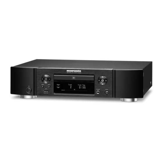
Network CD Player
ND8006
• For purposes of improvement, specifications and design are subject to change without notice.
• Please use this service manual with referring to the operating instructions without fail.
• Some illustrations using in this service manual are slightly different from the actual set.
Service Manual
Click here!
On-line service parts list
http://dmedia.dmglobal.com/Document/DocumentDetails/23921
ONLINE PARTS LIST
(P5)
WEB owner's manual
NA:
http://manuals.marantz.com/ND8006/NA/EN/index.php
EU:
http://manuals.marantz.com/ND8006/EU/EN/index.php
AP:
http://manuals.marantz.com/ND8006/AP/ZH/index.php
JP:
http://manuals.marantz.com/ND8006/JP/JA/index.php
Upload is planned for the time of a future press release.
BEFORE SERVICING THIS UNIT
ELECTRICAL
MECHANICAL
REPAIR INFORMATION
UPDATING
Please refer to the MODIFICATION NOTICE.
Confidential
Ver. 2
Advertisement
Table of Contents

Related Manuals for Marantz ND8006


Summary of Contents for Marantz ND8006
- Page 1 Service Manual Ver. 2 Network CD Player Click here! ND8006 On-line service parts list http://dmedia.dmglobal.com/Document/DocumentDetails/23921 ONLINE PARTS LIST (P5) WEB owner’s manual http://manuals.marantz.com/ND8006/NA/EN/index.php http://manuals.marantz.com/ND8006/EU/EN/index.php http://manuals.marantz.com/ND8006/AP/ZH/index.php http://manuals.marantz.com/ND8006/JP/JA/index.php Upload is planned for the time of a future press release. BEFORE SERVICING THIS UNIT...
- Page 2 BEFORE SERVICING THIS UNIT SAFETY PRECAUTIONS NOTE FOR SCHEMATIC DIAGRAM HANDLING THE SEMICONDUCTOR AND OPTICS WARNING AND LASER SAFETY INSTRUCTIONS ONLINE PARTS LIST Accessing the Parts List Searching Part Numbers or Ref. Numbers NOTE FOR PARTS LIST SERIAL NUMBER Serial Number Organization SKU Code of this Unit POST-SERVICE PRECAUTIONS Initializing this Unit...
-
Page 3: Safety Precautions
SAFETY PRECAUTIONS ◎ Make a safety check after servicing! The following items should be checked for continued protection of the customer and the service Check that all screws, parts and wires removed or disconnected when servicing have been put back technician. -
Page 4: Note For Schematic Diagram
NOTE FOR SCHEMATIC DIAGRAM WARNING AND LASER SAFETY INSTRUCTIONS WARNING: WARNING WAARSCHUWING Parts indicated by the z mark have critical characteristics. Use ONLY replacement parts recommended Alle IC’s en vele andere halfgeleiders zijn gevoelig All ICs and many other semi-conductors are voor elektrostatische ontladingen (ESD). -
Page 5: Note For Parts List
ONLINE PARTS LIST Accessing the Parts List Searching Part Numbers or Ref. Numbers (1) Access from the Service Manual You can search a Parts List for part numbers or Ref. numbers. ・ Click the URL link on the cover of the service manual. (1) Enter the part number or Ref. - Page 6 The 14-digit serial number that contains the code of the manufacturing plant and the manufacturing date. 14 digits Factory Manufactured Cumulative Year, month code code serial number The last Month 2digit of year (01 ~ 12) SKU Code of this Unit Product SKU SKU Code ND8006/U1B ND8006/N1B ND8006/N1SG ND8006/K1B ND8006/FN...
-
Page 7: Initializing This Unit
POST-SERVICE PRECAUTIONS Initializing this Unit Make sure to initialize this unit after replacing the microcomputer or any peripheral equipment, or the digital PCB. 1. Press the power operation button to turn off the power, and remove the AC plug from the socket. 2. -
Page 8: Schematic Diagrams
ELECTRICAL SCHEMATIC DIAGRAMS SCH01_uCOM SCH02_SRC, DIR, DAC-ADC SCH03_CD-DSP SCH04_X-MOS SCH05_Digital PLD SCH06_NET Module Connector SCH07_DAC, LINEOUT, HPAMP SCH08_VARIABLE OUT SCH09 STANDBY SMPS SCH10_MAIN POWER SUPPLY SCH11_DISPLAY PRINTED CIRCUIT BOARDS DIGITAL, FRONT, HP VOL, VOL BASE AUDIO, USB, P.SW POWER BLOCK DIAGRAM POWER DIAGRAM WIRING DIAGRAM SEMICONDUCTORS... - Page 9 SCHEMATIC DIAGRAMS SCH01_uCOM For reading of I2C received data P3V3_D P3V3_D P3V3_UCOM U1008 P3V3_UCO M P3V3_D SN74LV08APW P3V3_D R e g i o n i d e n t i f i c a t i o n r e s i s t o r l i s t U1008 Region N 1(EU)
- Page 10 SCH02_SRC, DIR, DAC-ADC P5V_D_SPDIF C2111 I 2C_SCL_DIR2 10uF I2C_SCL_DIR2 U2009 BIDIRECT C2106 JST2124-00-ABHN I2C_SDA_DIR2 I2C_SDA_DIR2 BIDIRECT 0 . 1 DIR_CLK R2169 DIR_CLK BIDIRECT DIR_CE DIR_CE VC C OPT OUT INPUT DIR_DIN DIR_DIN INPUT DIR_DOUT DIR_DOUT OUTPUT P3V3_D_AUDIO DIR_RESET DIR_RESET GND_D INPUT DIR2_DEMP DIR2_DEMP...
- Page 11 SCH03_CD-DSP TO A2 TO 7B To/Fro m To/From D i g i t a l P L D uCOM Sheet(1/6) S h e e t ( 5 / 6 ) CD_VREF P3V3_CD_D2 L3501 BLM21PG221 L3502 BLM21PG221 N3501 P1V5_CD_D1 P3V3_CD_D1 16FMN-BMTTR-A-TBT(LF)(SN) P1V5_CD_D2 16P-FFC-BAS P3V3_CD_D2...
- Page 12 SCH04_X-MOS D2501 D2506 OPEN OPEN USB_DP P3V3_USBB U2507 N2502 I NPUT USB_DN OPEN OPEN USBB_VBUS O UT P UT TPF86 R2514 OPEN M3-SIDE B2004 GND_D P3V3_USBB GND_D GND_D U2501 R2519 USB_DN MODE[0] USB_DN GND_D INPUT TLP185 P3V3_USB B USB_DP USB_DP MODE[1] INPUT R2515...
- Page 13 SCH05_Digital PLD R3077 OPEN PLD_SRC_MCK. PLD_SRC_MCK OUTPUT R3078 OPEN PLD_SRC_PBCK. PLD_SRC_PBCK OUTPUT R3079 OPEN TO B2 PLD_SRC_LRCK. PLD_SRC_LRCK OUTPUT R3080 OPEN PLD_SRC_DATA. PLD_SRC_DATA P3V3_D_PLD OUTPUT R3081 OPEN PLD_SRC_DBCK. PLD_SRC_DBCK OUTPUT L3002 11A121 R3082 OPEN To/Fro m PLD_SRC_DSDL. PLD_SRC_DSDL OUTPUT R3083 OPEN R3145 OPEN...
- Page 14 SCH06_NET Module Connector NET5V L4005 BLM21PG221 P5V_NET R4160 R4159 Net3.3V TPF99 NET5V_POWER U4006 C4032 Q4003 Q4004 OPEN L4003 FDC608PZ KRC404E-RTK GND_D BLM21PG221 NET_PLD_MCK. R4027 OPEN NET5V_POWER N4003 TPF98 R4028 OPEN R4085 OPEN C4035 R4150 SM2532CV-2x40-SMT-1-RT R4029 OPEN R4086 OPEN OPEN NET_FACT_RST C9014 C4036...
- Page 15 SCH07_DAC, LINEOUT, HPAMP +3.3D1 +5.25V L1006 OPEN L1011 11A121 +3.3D1 U1006 C1047 V+14A1 U1017 OUTPUT H.P_LCH OPEN 1000P C1044 U1003 R1006 TC74VHC74FT C1062 R1051 R1219 49.152MHz S1001 1CLR/ D1014 220/25 OPEN R1065 1SS302 G6K-2F-Y-TR 2CLR/ R1046 R1041 R1049 R1048 V+14A1 OUTPUT H.P_RCH Q1007...
- Page 16 SCH08_VARIABLE OUT 8U-210231-1(2/2) D1025 D1026 AUDIO UNIT Q1033 D1044 2SD2081 V+14A1 R1011 1SS302 (Audio Power BLOCK) Q1055 D1005 1(1W) Q1066 2SA1312(B) R1344 R1135 P_MUTE 11EQS10 47(1W) 2SAR293P V+14A2 OUTPUT C1085 R1186 2200/25 R1334 D1006 Q1044 11EQS10 KTA1266GR R1191 R1332 R1329 4.7K R1170 C1084...
- Page 17 SCH09 STANDBY SMPS 8U-210231-2(1/2) POWER UNIT (SMPS BLOCK) R5022 00D2061096022 OPEN AC100V_ L AC100V_N F810 0 T2AL/250V C5022 L5002 C5034 LF4ZBE273H 470P/250V FUSE_CLIP N5002 D5013 AC100V_L 2P-VHw D3SB60 T1001 R5028 H5001 H5002 1.1M CLT9Z064ZE R5029 10201010110AS 1.1M C5028 R5030 AC PLUG L5001 R5011 47/400...
- Page 18 SCH10_MAIN POWER SUPPLY 8U-210231-2(2/2) POWER UNIT +3.3V_NSW +5USBA S4002 MAIN POWER SUPPLY PWB(POWER) JSS2208A R4019 R4016 P_DOWN D4046 D4023 1SS355T Q4008 D4028 D4005 D4001 R4012 MM3Z3V6B C4031 4.7K Q4009 +6V_SMPS D4024 Q4007 KRA102S (10K-10K) D4006 C4022 R4002 OPEN 2SC4081 2.2/50 OPEN GND .
- Page 19 SCH11_DISPLAY N5006 N5008 TO N1001 TO N4007 N5008 8P-PH s 8U-210230-1 INPU RC-5_OUT FRONT CENTER PWB GNDF 2 Z5011 BUFFER(H=7mm) C5028 +3.3ST2 U5001 C5029 HM336R 0.01 +3.3ST2 C5030 Q5003 0. 1 KRA102S U5002 L5006 NJM2387DL3 +16DISP BLM21PG221 Vout Vadj B5001 C5005 CONT SRA21T3-SOLD...
-
Page 20: Printed Circuit Boards
PRINTED CIRCUIT BOARDS DIGITAL, FRONT, HP VOL, VOL BASE Lead-free Solder When soldering, use the Lead-free Solder (Sn-Ag-Cu). DIGITAL (A SIDE) DIGITAL (B SIDE) FRONT (A SIDE) FRONT (B SIDE) HP VOL (A SIDE) HP VOL (B SIDE) VOL BASE (A SIDE) - Page 21 AUDIO, USB, P.SW AUDIO (A SIDE) AUDIO (B SIDE) USB (A SIDE) USB (B SIDE) N5803 K2001 VOL CLK K2002 B2001 B1003 C2015 C2014 R2064 C1110 C1112 K1001 D2002 D2001 K1002 C1113 C1109 D5807 C2013 C2012 R2048 D5806 Q2023 C2005 C2004 C2003 C1171...
- Page 22 POWER POWER (A SIDE) POWER (B SIDE) K4001 N5001 K5001 S4002 Q5008 D5011 D5012 R5911 Q4010 Q4011 D5007 D5005 Q5007 C4021 R5910 B5004 R5010 B5009 C4029 C5006 R5009 C5005 C5033 C5004 C4035 D4045 R4020 D4037 R4018 R4022 U4006 U4008 U4002 U4001 C5032 R4006...
-
Page 23: Block Diagram
BLOCK DIAGRAM ND8006 Block Diagram R232C Flasher In RC-5 RC-5 Analog OUT Variable Digital PCB AUDIO PCB IN/OUT INT/EXT COAX OPT1 OPT2 COAX USB Type B CD Mecha UNIT GND_A GND_ CHASSIS CD Mecha GND_A GND_D GND_CHASSIS GND_A GND_A CD Moter... -
Page 24: Power Diagram
POWER DIAGRAM ND8006 Power diagram Standby Operation < 0.3W Network Control On Operation <4W Normal operation for digital power for audio power AC IN AP1150ADS33-L +6V_SMPS +3.3V_NSW P3.3VUCOM SMPS +3.3V +3.3V E2P ROM +3.3V I/O Expander SMPS_CNT +3.3V China K1B only S.Flash... -
Page 25: Wiring Diagram
WIRING DIAGRAM ND8006 WIRING DIAGRAM Wire Connector Connector only for Development (15) WiFi antenna x2 AC INLET N4002 5P-PH N4003 80P / N4004 42P N2503 11P-FFC N3002 27P-FFC N1001 27P-FFC 1.VBUS LEGO XMOS DEBUG 2.-D module 3.+D 8U-310224 4.GND 5.SHIELD... - Page 26 SEMICONDUCTORS Only major semiconductors are shown, general semiconductors etc. are omitted to list. The semiconductor which described a detailed drawing in a schematic diagram are omitted to list. 1. IC's R5F5631FDDFB (DIGITAL : U1004) Net- Normal Symbol Pin Name Description work STBY STBY...
- Page 27 Net- Net- Normal Normal Symbol Pin Name Description Symbol Pin Name Description work work STBY STBY STBY STBY Detect DC Protection (Audio B'D Power Supply Short) 112 P64 INSW CD Drive Limit SW Input 62 PC5 A_PW_SHORT (EVOL_CLK => A_PW_SHORT) 113 P63 OPSW CD Drive Opne SW Input...
-
Page 28: Terminal Function
Terminal Function Terminal Function I/O Expander (U1001, U1003, U1006), Open Drain Symbol Description Default Remarks Nor- Net- Addr. ND8006 Function Port Name Hardware PD/PU Detail of Function work Port name DSP VCO - EFM and PLCK Phase difference STBY. STBY. - Page 29 Symbol Description Default Remarks Symbol Description Default Remarks Focus Error signal / Sub beam add signal FSMoNiT 3AI/F output pin(monitor pin/GND) DVSS3R Grounding pin for 3.3V Muiti-Bit DAC circuit RFZi 3AI/F R channel audio output pin of Audio DAC. RFRP 3AI/F 3AI/F Bulit-in serises R=500...
- Page 30 BA5810FP/FM 光ディスク IC ブロックダイアグラム BA5810 (DIGITAL : U3502) Symbol Description Default Remarks VDD3 Power Supply pin for 3.3V Digital circuit CH1~ POWVCC 34 CMOS Port (CH3, CH4) MUTE BUS0 Microprocessor I/F data input/output pin 0 Schmitt input 3I/F Refer to [1.2 Pin Assinment Table] CMOS Port 7.5k −...
- Page 31 *For adjustable version only. AK4458VN 40 +105 C (Exposed pad is connected to ground) Figure 1. Typical Application Circuit 40 +85 C (Exposed pad is open) Figure 1. Typical Application Circuit 48-pin QFN (0.5mm pitch) AKD4458 Evaluation Board for AK4458 NCP380 (DIGITAL : U4003) AK4458VN (DIGITAL : U2001) Pin Configurations...
- Page 32 [AK4458] FUNCTIONAL BLOCK DIAGRAM No. Pin Name I/O Function PD State 4. Block Diagram and Functions CAD0_I2C Chip Address 0 Pin in I2C Bus serial control mode Chip Select Pin in 3-wire serial control mode LDOE TVDD VDD18 DVSS AVDD AVSS Hi-Z Audio Data Format Select in Parallel control mode.
- Page 33 PCM9211 PCM9211 (DIGITAL : U2002) www.ti.com SBAS495 – JUNE 2010 PIN CONFIGURATIONS DESCRIPTION NAME PT PACKAGE LQFP-48 TOLERANT (TOP VIEW) MS/ADR1 Software control I/F, SPI chip select / I2C slave address setting1(2) MODE Control mode setting, (see the Serial Control Mode section, ERROR/INT0 VDDRX Control Mode Pin Setting)
-
Page 34: Pin Functions
PCM9211 PCM9211 BLOCK DIAGRAM LC89091JA (DIGITAL : U2005) www.ti.com SBAS495 – JUNE 2010 BLOCK DIAGRAM FILT AUXIN 0 AUTO RXIN7 RXIN 0 RXIN0 SCKO DOUT RXIN 1 RXIN1 MAIN OUTPUT RXIN 2 RXIN2 AUXIN0 LRCK SCKO/ BCK/LRCK PORT RXIN 3 RXIN3 AUXIN1 DOUT... - Page 35 XMOS (XS1-U8A-128-FB217) (DIGITAL : U2502) Module Name Function Type Active Properties X0D14 P16A P32A — X0D15 — P16A P32A X0D16 — P16A X0D17 P16A — X1D05 X1D06 X1D07 X1D08 X1D09 X1D10 X1D11 X1D12 X1D13 X1D14 X1D15 X1D16 X1D17 X1D18 X1D19 X1D20 X1D21 X1D22...
- Page 36 ES9016K2M (AUDIO : U1019) NJU72343_J (AUDIO : U2001) DGND DVDD N.C. DGND ES9016K2M N.C. DVCC 28-QFN ADDR VCCA AVCCDAC XI (MCLK) N.C. No. Symbol Function No. Symbol Function AREF Analog reference potential DATA IC control data input Address selection CLOCK IC control clock input PIN DESCRIPTIONS InA2...
-
Page 37: Oled Display
ICE3BR4765J (POWER : U5004) 2. OLED DISPLAY MXS4035A n.c. Drain Drain Terminal Function Symbol Function MXS4035A IO Interfaces extended Blanking & Auto-restart FeedBack Current Sense/ ® 650V l CoolMOS Source Drain 650V l CoolMOS ® Drain Drain 650V l CoolMOS ®... - Page 38 3. Remote Code Table ND8006 (RC-5) Extended Code RC-5/RC-5 Ext. ND8006 must receive following codes. RC001PMND Code1: AMP (Initial) Code2: Variable These codes are not included in the RC001PMND KEY No. Key Name System Command Extension System Command Extension POWER (Network) <=...
- Page 39 MECHANICAL DISASSEMBLY Flowchart 1. TRAY PANEL 2. MECHA ASSY 3. DIGITAL PCB 4. FRONT ASSY 5. POWER PCB 6. AUDIO PCB EXPLODED VIEW OF CD MECHANISM UNIT EXPLODED VIEW PACKING VIEW...
- Page 40 DISASSEMBLY Flowchart • Remove each part following the flow below. • Reassemble the removed parts in the reverse order. • Read "SAFETY PRECAUTIONS" before reassembling the removed parts. • If wire bundles are removed or moved during adjustment or part replacement, reshape the wires after completing the work. Failure to shape the wires correctly may cause problems such as noise. •...
-
Page 41: Tray Panel
• The photographs with no shooting direction indicated were taken from the top of the unit. (1) Open the TRAY PANEL and remove the door. • Photos of ND8006 N1SG are used in this manual. View from the bottom The viewpoint of each photograph (Shooting direction : X) [View from the top] ↓Shooting direction: B↓... -
Page 42: Mecha Assy
2. MECHA ASSY 3. DIGITAL PCB Proceeding : TOP COVER → TRAY PANEL → MECHA ASSY Proceeding : TOP COVER → DIGITAL PCB (1) Remove the screws. Remove the connector. Remove the TAPE. (1) Remove the screws. Remove the connector. Remove the STYLE PIN. ↓Shooting direction: B↓... - Page 43 5. POWER PCB Proceeding : TOP COVER → DIGITAL PCB → POWER PCB (1) Remove the screws. Remove the connector. Remove the STYLE PIN. STYLE PIN x3 N4002 N4003 N4007 N4001 N5002 6. AUDIO PCB Proceeding : TOP COVER DIGITAL PCB → AUDIO PCB →...
-
Page 44: Exploded View Of Cd Mechanism Unit
EXPLODED VIEW OF CD MECHANISM UNIT http://dmedia.dmglobal.com/Document/DocumentDetails/23921 Parts List :... -
Page 45: Exploded View
EXPLODED VIEW http://dmedia.dmglobal.com/Document/DocumentDetails/23921 Parts List : ▽ ×6 ▽ ▽ ☆ ▼ ◎ ×2 ▼ ★ ×2 ◎ ☆ ▼ ▼ ★ ▽ ☆ ▼ ▼ ◎ ★ ×3 ☆ ▽ ×2 ×3 ☆ ×3 ◎ ★ ▼ ▼ ☆ ▽... -
Page 46: Packing View
PACKING VIEW http://dmedia.dmglobal.com/Document/DocumentDetails/23921 Parts List : P02-2 UK plug (UK Only) P02-1 P03-1... -
Page 47: Repair Information
REPAIR INFORMATION TROUBLE SHOOTING SPECIAL MODE 1. POWER Special mode setting button 2. OLED 1. Selecting the Mode1 for Service-related 3. No Remote Control Reception 1-1. Version Display Mode 4. Audio PCB Abnormalities and no Audio Output (Line Out, Variable Out, H/P 1-2. - Page 48 TROUBLE SHOOTING 1. POWER 1.1. The unit does not power on When the power supply is connected to an AC power inlet, does Can the device be started up and can "Protection History" from the on/standby indicator on the top of the power switch blink red Check the protection type.
- Page 49 1.3. Power Supply Voltage Abnormalities Are any of the Power PCB power supply ICs functioning abnor- mally? Check the output voltage FRONT PCB form POWER PCB Replace any defective parts or the Power PCB. If the input voltage of all the power supply ICs is 0V, proceed to Are there large deviations in the output voltage? "NO".
- Page 50 2. OLED 2.1. OLED is not lit Check if the connection is as indicated in the Turn on the power and check the waveform of Check the connection. wiring diagram and adjust the FFC wiring if the digital signal. The System uCOM is malfunctioning or latched. Has a contact failure occurred or is a connector necessary.
- Page 51 3. No Remote Control Reception Check that you are using a [RC001PMND] remote control and replace the batteries. There is a [Q5003] malfunction if a square wave Is the switch on the [REMOTE CONTROL] input is not output to the Front PCB [Q5003] collector output back panel set to [EXTERNAL]? Is a square wave output when the power is on in the same way.
- Page 52 4. Audio PCB Abnormalities and no Audio Output (Line Out, Variable Out, H/P Out) This section details items to check if the digital audio signal is being correctly input to the Audio PCB DAC IC [U1019]. Is the Master Clock waveform indicated below being input to the Audio PCB DAC IC [U1019: 7 pin] in Check if the Clock output from the crystal oscillator [U1001, U1003 and U1016] output terminals the function indicated below? corresponds with the table to the left.
- Page 53 There may be an abnormality in the differential synthesis of the last Are signals output from all of the I/V converter circuit outputs (4 Is no audio output from the line out, variable out or H/P out output stage of the I/V converter or HDAM circuits. circuits) of the last stage of DAC IC [U1019]? terminals when "Variable Out"...
- Page 54 5. Cannot Play CDs Electricity first passes through the CD DSP, motor driver IC and CD mechanism when the function is turned to CD. This section details items to check if the audio signal is being correctly input. Turn power and communication of all other functions off. Check the input signal.
- Page 55 Check the connection. Check if the connectors are connected as indicated in the wiring diagram and adjust the connections if Has a contact failure occurred or is a connector missing? necessary. POWER PCB [N4006] If this does not re-establish contact in the wiring, replace the Wire Assy unit or the circuit board which DIGITAL PCB [N3504] the wires are mounted on.
- Page 56 Check the [C2513] 100uF/6.3 + terminal voltage. Does the file type (PCM or DSD) and sampling frequency display on Is the problem the "marantz" PC driver, software settings or USB Install and set up the driver correctly as indicated in the instruction...
- Page 57 7. No Audio Output during USB File Playback (USB-A input), File Playback on a Server or Internet Radio and Bluetooth Playback Before testing circuit operation, check if the file to be played back is in a supported format and network settings are correct. When playing back an audio file or streaming, are digital audio waveforms output from the LEGO There is a malfunction in communication between the LEGO Module [N4003] and System uCOM Module [N4003]?
- Page 58 8. No Audio Output during OPT or COAX Playback Is the S/PDIF signal input to DIR [U2002]? Check for an OPT or COAX input malfunction and input buffer IC DIGITAL PCB [U2007] power supply voltage [3.3V] and input output to deter- [R2023]COAX IN, [R2039]OPT1 IN, [R2037]OPT2 IN mine the location where the S/PDIF signal is interrupted.
- Page 59 MEASURING METHOD AND WAVEFORMS 1. DIGITAL PCB test point Measuring Disc : 4822 397 30184 TCD-784 (It is recommended to use extension wires between the probe and test points.) DIGITAL PCB : test point q RFEQO Q1 LOAD+ W1 CD_PLD_LRCK w RFO Q2 LOAD- W2 CD_PLD_DATA...
- Page 60 WAVEFORMS 1. DISC PLAY RF WAVEFORM(EYE-PATTERN) 2. DISC DETECTION 3. TOC READ 4. FOCUS ADJUSTMENT 1.1 CD(TCD-784)Play 2.1 CD(TCD-784)DISC DETECTION 3.1 CD(TCD-784)TOC READ 4.1 CD(TCD-784)FOCUS ADJUSTMENT ②RFO ②RFO ③FSMONIT 200mV 200mV ③FSMONIT ④FOO ④FOO ①RFEQO ⑤TEI 500Mv ⑤TEI 500Mv ⑥ TRO ⑥...
- Page 61 9-12 OPSW CLSW_LOAD+_LOAD- 13-15 DAC input DSD BCK_DSDL_DSDR 23-25 Digital input playback PCM BCK_LRCK_DATA 26-28 Network playback PCM BCK_LRCK_DATA o OPSW Q3 DSD_BCK W3 DIR1_PLD_PBCK W6 NET_PLD_I2S0_BCK Q0 CLSW OPEN CLOSE Q4 DSDL W4 DIR1_PLD_LRCK W7 NET_PLD_I2S0_LRCK Q1 LOAD+ Q5 DSDR W5 DIR1_PLD_DATA W8 NET_PLD_I2S0_DATA Q2 LOAD-...
-
Page 62: Protection Of The Ld
NOTES ON HANDLING AND REPLACEMENT OF THE LASER PICK-UP 1. Protection of the LD Solder a part of the LD circuit to short-circuit. After connecting the circuit, remove the soldering form. Precautions when handling the laser CD mechanism 2. Precautions when handling the laser CD mechanism •... -
Page 63: Special Mode Setting Button
SPECIAL MODE Special mode setting button b No. 1: Insert the AC plug while pressing button "A", and wait for more than 3 seconds. b No. 2 - 4: Insert the AC plug while pressing buttons "A" and "B" together, and wait for more than 3 seconds. b No. - Page 64 1. Selecting the Mode1 for Service-related 1.1. Actions Selecting Each Mode. 1.2. Starting up Insert the AC plug while pressing button "POWER", and wait for more than 3 seconds. Executes an update for the entire device via DPMS. Select the desired mode using the "CURSOR f / d " button, then press the "ENTER" button to confirm. 1.3.
- Page 65 o HEOS Locale 1-1. Version Display Mode 1-1.1. Actions Version information is displayed when the device is started in this mode. 1-1.2. Starting up Q0 Ether Mac Address Insert the AC plug while pressing button "POWER", and wait for more than 3 seconds. Release button "POWER"...
-
Page 66: Protection History Display Mode
・ Display when protection has been activated 1-2. IR Control Test This function is used to check IR control operations. 1-2.1. Starting up Insert the AC plug while pressing button "POWER", and wait for more than 3 seconds. Cause : Power supply short circuit detected in the power supply board Release button "POWER"... -
Page 67: Cd Test Mode
1-5. CD Test Mode 1-5-1. Disc mounting Test the CD mechanism. Press the " 5 " button to open the tray. ※ Even if a disc is loaded, operation will not begin unless open is changed to closed. 1-5.1. Starting up Insert the AC plug while pressing button "POWER", and wait for more than 3 seconds. - Page 68 (5) READ SUB CODE (playback sound output) 1-5-5. All servo on ・ Displays the BER (Block Error Rate) for 1 second. ・ Press the "CURSOR d " button to turn on the all servos and perform auto adjustment. After auto ・...
- Page 69 1-5-7. Displaying the laser current 1-6. Heat run Mode ・ Press and hold the " 9 " button for at least 1 second while stopped(1-5-4. Stop) to turn the laser ON ・ Heat run mode is run for the selected mode. and measure and display the laser current.
- Page 70 1-6-1. Heat run normal mode 1-6-3. Heat run Chucking mode Select the "HR Normal" using the "CURSOR f / d " button, then press the "ENTER" button to confirm. Select the "H.R.Chucking" using the "CURSOR f / d " button, then press the "ENTER" or " 13 " button to ・...
-
Page 71: Error Display
1-6-4. Error display 1-7. Initialize ・If an error occurs, operations stop and the error display is displayed. Initializes all MCU and network module backup data. NOTE: If initialization is executed in LEGO Off mode, cancel LEGO off mode then reset the LEGO Net- Operation button (only for this unit) work. -
Page 72: Tray Lock Mode
2. Factory Initialization Mode 4. Tray Lock Mode Initialize backup data of the MCU. Disables the OPEN/CLOSE buttons. 5.1. Actions 2.1. Starting up Set or cancel the tray lock. 1. Press the power operation button to turn off the power, and remove the AC plug from the socket. When the tray lock is set, the "... - Page 73 5. Network Function Reset Initializes network settings. 5.1. Actions The following items are initialized. (1) Network setup (2) Friendly Name (3) Auto Update setting (4) Allow Update setting (5) Time Zone setting (6) Queue list (7) Internet Radio recently played station (8) Quick Select playback station (9) AirPlay Password (10) Bluetooth Pairing History...
- Page 74 (3) When saving of the log package fails, "USB FAILED" appears in the display for 5 seconds, regardless 6. Selecting the Mode2 for Service-related of whether the upload to the server was successful. Selecting Each Mode. 6.2. Starting up While the power is on, hold down buttons "POWER" and "ENTER" for at least 3 seconds. (1) "LEGO Log Capture Mode"...
- Page 75 UPDATING PROCEDURE AFTER REPLACING THE PCB. PROCEDURE AFTER REPLACING THE U-COM, ETC. FIRMWARE UPDATE PROCEDURE 1. Items necessary for update 2. Update preparation with a USB flash drive (U1004, U3001, NETWORK MODULE) 3. Update method when the DIGITAL PCB or network module is replaced (Using a USB flash drive U1004, U3001, NETWORK MODULE) 4.
- Page 76 PROCEDURE AFTER REPLACING THE PCB. PROCEDURE AFTER REPLACING THE U-COM, ETC. The procedure after replacing the printed circuit boards is as follows. The procedure after replacing the u-COM (microprocessor) is as follows. (1) Change the resistor for setting the region. Implement the update method when the DIGITAL PCB or network module is replaced.
-
Page 77: Firmware Update Procedure
LED installed. Internet Connection by Broadband Circuit Modem Via OTA Router Ethernet cable (CAT-5 or greater is recommended) Marantz XM Windows Driver v3.X.X for Windows10 Personal Computer Marantz XM Windows Driver v2.X.X USB-B Update for Windows8-1_8_7 ModelName_DFU_MX25L4006E_ USB cable (A type-B type) vXXX.bin... - Page 78 2. Update preparation with a USB flash drive (U1004, U3001, NETWORK MODULE) You can update the firmware by downloading the latest version with USB flash drive. 2.1. Connecting to the USB flash drive (1) Preparation ・ Windows PC ・ USB flash drive format : Prepare a USB flash drive formatted in FAT16 or FAT32. b We recommend a USB flash drive that has an LED installed.
-
Page 79: Start The Update
3. Update method when the DIGITAL PCB or network module is replaced (Using a USB flash drive U1004, U3001, NETWORK MODULE) 3.1. File structure on USB flash drive (5) USB Update starts automatically. The Standby LED lights red. DIGITAL PCB or network module is replaced onto the USB flash drive in the following structure. Display during USB update After unzipping the files, store them in the root of the same USB flash drive. - Page 80 4. Update Method for Service Region Settings (U1004, U3001, NETWORK MODULE) Copy the Service Region Settings from the USB flash drive to this unit. (5) Copy the files created on the USB flash drive. 4.1. Creating a Service Region Settings file (1) Click [Start button] - [Accessories] - [notepad] on the PC to launch the notepad.
- Page 81 5. Normal Firmware Update Method from USB Flash Drive (U1004, U3001, NETWORK MODULE) 5.1. File structure on USB flash drive (4) Insert the USB flash drive into the USB port. Copy the normal update files onto the USB flash drive in the following structure. Download firmware After unzipping the HW component USB update files for the target model and LEGO USB update files, in USB flash drive.
-
Page 82: Network Connection
6. Normal Firmware Update Method from OTA (U1004, U3001, NETWORK MODULE) 6.2. Check and update the firmware Download the latest firmware from our website and update the firmware. 6.1. Network Connection Check if there is a firmware update available. It is also possible to check approximately how long the (1) System Requirements update will take. - Page 83 7. About the error codes (U1004, U3001, NETWORK MODULE) See the table below for details on error codes and solutions when updating the firmware. Device ID table Error codes are displayed in 4 digits, : DeviceID, : ErrorCode). YYXX Device ID ( YY ) Device Name Display General...
- Page 84 (3) Move the dedicated driver to the installed folder. (If the installation location of the dedicated driver has not been changed, it is stored in ←ーー(7) "C:\Program Files\Marantz\Marantz_USB_Driver". ) (4) Rename the binary file for USB update as shown below. ModelName_DFU_MX25L4006E.bin (Ex.) ND8006_DFU_MX25L4006E.bin (Do not include a hyphen in the model name.)
- Page 85 Copyright © 2017 D&M Holdings Inc. All Rights Reserved.
Need help?
Do you have a question about the ND8006 and is the answer not in the manual?
Questions and answers
Здравствуйте. Почему в Marantz ND8006 в левом канале меньше высоких чем в правом? Спасибо.