Advertisement
Quick Links
User's Guide
Isolated DC/DC Converters ICs
Built-in Automotive Switching MOSFET
Isolated Flyback Converter ICs
BD7F205EFJ-C Evaluation Board
BD7F205EFJ-EVK-001
Overview
This evaluation board outputs an isolated 6.2 V, 16.5 V and 6.2 V voltage from an input of 8 V to 32 V, and can output a maximum
output power 6 W.
BD7F205EFJ-C is an isolated flyback converter that does not require a photocoupler.
Feedback circuit by the transformer's tertiary winding or photocouplers becomes unnecessary, contributing to reduction of set
parts.
It also has a number of built-in protection functions that enable the design of isolated power supply applications for high reliability.
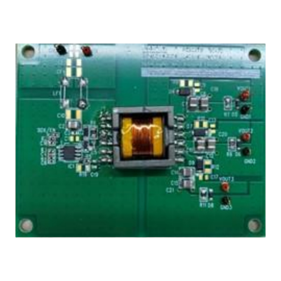
Figure 1. BD7F205EFJ-EVK-001
© 2022 ROHM Co., Ltd.
65UG028E Rev.001
1/25
2022.7
Advertisement

Subscribe to Our Youtube Channel
Related Manuals for Rohm BD7F205EFJ-C


Summary of Contents for Rohm BD7F205EFJ-C
- Page 1 This evaluation board outputs an isolated 6.2 V, 16.5 V and 6.2 V voltage from an input of 8 V to 32 V, and can output a maximum output power 6 W. BD7F205EFJ-C is an isolated flyback converter that does not require a photocoupler. Feedback circuit by the transformer’s tertiary winding or photocouplers becomes unnecessary, contributing to reduction of set parts.
- Page 2 Output current 1 OUT1 Output current 2 OUT2 Output current 3 OUT3 Maximum output power Standby power = 0 A V = 12 V INSTBY Power Supply Efficiency η = 2 W © 2022 ROHM Co., Ltd. 65UG028E Rev.001 2/25 2022.7...
- Page 3 (7) Turn on the output of the DC power supply. (8) Check that the DC voltmeter display is at the set voltage. (9) Activates the load. Figure 2. Connection Diagram © 2022 ROHM Co., Ltd. 65UG028E Rev.001 3/25 2022.7...
- Page 4 Operation starts when the VIN pin voltage exceeds UVLO detect voltage of 3.4 V (Typ) and SDXEN pin Enable pin voltage of 2.0 V (Typ). The circuit diagram of the demonstration board is shown in the figure below, and the parts list is shown on page 12. Figure 3. Circuit diagram © 2022 ROHM Co., Ltd. 65UG028E Rev.001 4/25 2022.7...
- Page 5 Shutdown/Enable control pin L_COMP Load current compensation value setting pin Output voltage setting pin Output voltage setting pin N.C. No Connect Switching output pin Power input terminal EXP-PAD Rear heat dissipation pin © 2022 ROHM Co., Ltd. 65UG028E Rev.001 5/25 2022.7...
- Page 6 80.0 VIN=32V 75.0 70.0 65.0 VIN=8V VIN=12V 60.0 VIN=18V VIN=32V 55.0 50.0 IOUT[A] IOUT1[A] Figure 7. Output Voltage3 vs Output Current1 Figure 8. Efficiency vs Output Current1 IOUT2=30mA, IOUT3=50mA IOUT2=30mA, IOUT3=50mA © 2022 ROHM Co., Ltd. 65UG028E Rev.001 6/25 2022.7...
- Page 7 80.0 VIN=32V 75.0 70.0 65.0 VIN=8V VIN=12V 60.0 VIN=18V VIN=32V 55.0 50.0 IOUT[A] IOUT1[A] Figure 11. Output Voltage3 vs Output Current1 Figure 12. Efficiency vs Output Current1 IOUT2=100mA, IOUT3=300mA IOUT2=100mA, IOUT3=300mA © 2022 ROHM Co., Ltd. 65UG028E Rev.001 7/25 2022.7...
- Page 8 Figure 13. Output Voltage1 vs Input Voltage IOUT1=100mA, IOUT2=100mA, IOUT3=300mA IOUT1=100mA, IOUT2=100mA, IOUT3=300mA VOUT3 Freq VIN[V] VIN[V] Figure 15. Output Voltage3 vs Input Voltage Figure 16. Frequency vs Input Voltage IOUT1=100mA, IOUT2=100mA, IOUT3=300mA IOUT1=100mA, IOUT2=100mA, IOUT3=300mA © 2022 ROHM Co., Ltd. 65UG028E Rev.001 8/25 2022.7...
- Page 9 OUT3 Figure 21. Output voltage ripple Waveform Figure 22. Output voltage ripple Waveform VIN = 12 V / IO1,2,3=0.1, 0.05, 0.1 A VIN = 12 V / IO1,2,3=0.3, 0.1, 0.3 A © 2022 ROHM Co., Ltd. 65UG028E Rev.001 9/25 2022.7...
- Page 10 500us/div 10ms/div (10V/div) (10V/div) (10V/div) (20V/div) (20V/div) (20V/div) (2A/div) (2A/div) (20V/div) (2A/div) Figure 27. VOUT Short Waveform Figure 28. VOUT Short Waveform (ZOOM) Vin = 15 V Vin = 15 V © 2022 ROHM Co., Ltd. 65UG028E Rev.001 10/25 2022.7...
- Page 11 In this case, when Ta = 125 °C, Tj = 146 °C, and Tj = 150 °C is not reached, so it can be judged that there is no problem in the whole temperature range. © 2022 ROHM Co., Ltd. 65UG028E Rev.001 11/25 2022.7...
- Page 12 User's Guide Circuit diagrams (Condition) V = 8 V to 32 V, V = 16.5 V, 0.2 A Figure 32. BD7F205EFJ-EVK-001 Schematic Bill of Materials *Parts are subject to change without notice. © 2022 ROHM Co., Ltd. 65UG028E Rev.001 12/25 2022.7...
- Page 13 BD7F105EFJ-EVK-001 User's Guide Transformer specifications Manufacturer : Sumida Electric Co., Ltd. https://job.mynavi.jp/conts/n/sp/23/54430_23sumida/ Product name: CEFD2010-00399-T381R ◼ External Dimensions ◼ Recommended Land ■ Terminal connection diagram © 2022 ROHM Co., Ltd. 65UG028E Rev.001 13/25 2022.7...
- Page 14 BD7F105EFJ-EVK-001 User's Guide Transformer Specifications-continued ■ Winding wire and linear/linear type ■ ELECTRICAL CHARACTERISTICS © 2022 ROHM Co., Ltd. 65UG028E Rev.001 14/25 2022.7...
- Page 15 + 0.5 6.2�� + 0.6�� For this reason, there is no problem in this design. of this designer is 0.44 and 0.70 or less, so it is judged without any problem. © 2022 ROHM Co., Ltd. 65UG028E Rev.001 15/25 2022.7...
- Page 16 �� : Constant representing the depth of the current continuous mode (When designing, use k = 0.25 as a guide.) Ipeak Primary current Ippk Secondary current Ispk time Figure 34. SW waveform : Primary transformer peak current �� ������ : Primary transformer bottom current �� ���� © 2022 ROHM Co., Ltd. 65UG028E Rev.001 16/25 2022.7...
- Page 17 = �� × ( �� �� �� �� �� = 21���� × (0.92) = 18���� �� From the above, we will proceed with the design as Lp:18μH, Ls:21μH in this design. © 2022 ROHM Co., Ltd. 65UG028E Rev.001 17/25 2022.7...
- Page 18 �� ���� �� �� �� ���� ���� ���� : FB pin inrush current �� ���� : FB terminal voltage �� ���� : External resistor between FB and SW pins �� ���� © 2022 ROHM Co., Ltd. 65UG028E Rev.001 18/25 2022.7...
- Page 19 Also, when the transformer is not coupled, the number of turns of N is shifted, which causes the output voltage to decrease. Therefore, finally adjust the output voltage by checking the actual device. © 2022 ROHM Co., Ltd. 65UG028E Rev.001 19/25 2022.7...
- Page 20 4. Input Capacitor Use a ceramic capacitor for the input capacitor and place it as close to the IC as possible. Capacitance of the capacitor should be 10 μF or more. © 2022 ROHM Co., Ltd. 65UG028E Rev.001 20/25 2022.7...
- Page 21 Therefore, it should be set lower enough than this R . Adjust this resistance value in the actual evaluation. When selecting a resistor, pay attention to the rated power of the resistor. © 2022 ROHM Co., Ltd. 65UG028E Rev.001 21/25...
- Page 22 �� //�� ������/���� : Target operations start VIN voltage �� ����_������������ : Enable volt1 �� ����1 : Partial pressure resistance between R and R inside the ICs �� //�� SDX/EN ������/���� © 2022 ROHM Co., Ltd. 65UG028E Rev.001 22/25 2022.7...
- Page 23 × �� × �� [µA] �������������� ��_�������� ��_�������� ����(������) Resistor connected to the L_COMP pin �� ��_�������� Average current flowing through the SW pin �� ����(������) Fixed value inside the IC L_COMP © 2022 ROHM Co., Ltd. 65UG028E Rev.001 23/25 2022.7...
- Page 24 Be sure to check the output voltage characteristics in the application evaluation and adjust the L_COMP terminal resistor as necessary. When compensation is not performed, short the L_COMP pin to GND. © 2022 ROHM Co., Ltd. 65UG028E Rev.001 24/25 2022.7...
- Page 25 BD7F105EFJ-EVK-001 User's Guide Revision history Date Plate Content of change 1st.Aug.2022 © 2022 ROHM Co., Ltd. 65UG028E Rev.001 25/25 2022.7...
- Page 26 Products. ROHM does not grant you, explicitly or implicitly, any license to use or exercise intellectual property or other rights held by ROHM or any other parties. ROHM shall have no responsibility whatsoever for any dispute arising out of the use of such technical information.
Need help?
Do you have a question about the BD7F205EFJ-C and is the answer not in the manual?
Questions and answers