Z3 Technology HE4K-DCK-10 Hardware Specification
4k h.265 & h.264 video encoder system
Hide thumbs
Also See for HE4K-DCK-10:
- User instructions (76 pages) ,
- Connection instructions (3 pages) ,
- Instructions manual (14 pages)
Table of Contents
Advertisement
Quick Links
Hardware Specification
4K H.265 & H.264 Video Encoder System
HE4K-DCK-10
Model Name:
DOC-USR-0100-01
Manual Version 1.00.00
July 20, 2016
Before attempting to connect or operate this product, please read these instructions carefully and save this manual for future use.
Copyright © 2016 Z3 Technology, LLC. All rights reserved.
This document contains proprietary and confidential information of Z3 Technology, LLC ("Z3"). This document may not be used, reproduced,
disclosed, or disseminated to anyone without the prior written approval of an authorized representative of Z3.
Z3 Technology, LLC incorporates HDMI® technology. The terms of HDMI and HDMI High-Definition Multimedia Interface, and
the HDMI Logo are trademarks or registered trademarks of HDMI Licensing LLC in the United States and other countries.
Sony is a trademark of Sony Corporation. All product or service names mentioned herein are the trademarks of their respective owners.
Advertisement
Table of Contents

Subscribe to Our Youtube Channel
Related Manuals for Z3 Technology HE4K-DCK-10


Summary of Contents for Z3 Technology HE4K-DCK-10
- Page 1 Copyright © 2016 Z3 Technology, LLC. All rights reserved. This document contains proprietary and confidential information of Z3 Technology, LLC ("Z3"). This document may not be used, reproduced, disclosed, or disseminated to anyone without the prior written approval of an authorized representative of Z3.
- Page 2 HE4K-DCK-10 HARDWARE SPECIFICATION CONFIDENTIAL DOC-USR-0100-01 Revision History Version Date Change Note Author 1.00.00 07/20/2016 Original Document ____________________________________________________________________________________ Z3 Technology, LLC ♦ 100 N. 8th St. STE 250 ♦ Lincoln, NE 68508-1369 USA ♦ +1.402.323.0702...
-
Page 3: Table Of Contents
HARDWARE FEATURES ....................13 7.1 Interface Front End PCB .................... 13 7.2 Main Encoder PCB ....................19 7.3 I/O Jack and PoE PCB ....................24 ____________________________________________________________________________________ Z3 Technology, LLC ♦ 100 N. 8th St. STE 250 ♦ Lincoln, NE 68508-1369 USA ♦ +1.402.323.0702... - Page 4 Figure 5: Interface Front End PCB Hardware Layout ..............13 Figure 6: Layout of the I/O Jack and PoE PCB Production Version ..........24 ____________________________________________________________________________________ Z3 Technology, LLC ♦ 100 N. 8th St. STE 250 ♦ Lincoln, NE 68508-1369 USA ♦ +1.402.323.0702...
- Page 5 Table 16 Main Encoder PCB and I/O Jack PCB Mating ..............24 Table 17 I/O Jack and PoE PCB Connectors ................25 ____________________________________________________________________________________ Z3 Technology, LLC ♦ 100 N. 8th St. STE 250 ♦ Lincoln, NE 68508-1369 USA ♦ +1.402.323.0702...
-
Page 6: General Description
DOC-USR-0100-01 GENERAL DESCRIPTION The HE4K-DCK-10 is an H.265/HEVC, H.264 and MJPEG video encoder designed to be a companion to the Sony FCB-ER8300 4K block camera. It is capable of accepting 4K UHD video from the camera at 30 frames per second and producing IP streams that can be sent on a standard Ethernet cable. -
Page 7: Features
Web-based user interface for configuration Low Power Optional chassis for block camera and encoder assembly available* * Contact Z3 Technology for more information. ____________________________________________________________________________________ Z3 Technology, LLC ♦ 100 N. 8th St. STE 250 ♦ Lincoln, NE 68508-1369 USA ♦ +1.402.323.0702... -
Page 8: Physical
Sony FCB-ER8300 camera block. Figure 2: HE4K-DCK-10 Physical Block Diagram (Chassis & Camera Not Included) ____________________________________________________________________________________ Z3 Technology, LLC ♦ 100 N. 8th St. STE 250 ♦ Lincoln, NE 68508-1369 USA ♦ +1.402.323.0702... -
Page 9: Figure 3: He4K-Dck-10 Block Diagram
HE4K-DCK-10 HARDWARE SPECIFICATION CONFIDENTIAL DOC-USR-0100-01 Figure 3 shows a block diagram of the HE4K-DCK-10 system. Figure 3: HE4K-DCK-10 Block Diagram ____________________________________________________________________________________ Z3 Technology, LLC ♦ 100 N. 8th St. STE 250 ♦ Lincoln, NE 68508-1369 USA ♦ +1.402.323.0702... -
Page 10: Thermal Considerations
Table 1 Temperature Critical Components When designing the thermal dissipation for the HE4K-DCK-10 it is important to consider the thermal behavior of all parts of the system, including the PCBs, enclosure, camera block, etc. While the majority of the power dissipation comes from the components listed in the table above, other parts such as the DDR chip, power IC’s and inductors also contribute some power to the system and cause... -
Page 11: Connecting The He4K-Dck-10 To A Sony Fcb-Er8300 Camera
Z3 Technology provides the correct cable as part of the HE4K-DCK-RPS. Please ONLY USE THE CABLE PROVIDED BY Z3 TECHNOLOGY to connect the Sony FCB-ER8300 to the I/F Front End PCB of the HE4K-DCK- The correct cable is the “straight thru”, with pin 1 connecting to pin 1. The figure below shows the straight cable. -
Page 12: Specifications
0 °C 50 °C Open air, unobstructed air flow Storage Temperature -20 °C 80 °C 20% to 70% RH, non-condensing Table 2 Specifications ____________________________________________________________________________________ Z3 Technology, LLC ♦ 100 N. 8th St. STE 250 ♦ Lincoln, NE 68508-1369 USA ♦ +1.402.323.0702... -
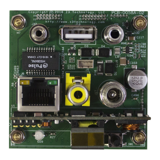
Page 13: Hardware Features
CONFIDENTIAL DOC-USR-0100-01 HARDWARE FEATURES The following section describes the I/O jacks and controls of the three board HE4K-DCK-10 camera dock video encoder system. 7.1 Interface Front End PCB The Interface Front End PCB converts the video format provided by the FCB-ER8300 or a Micro-HDMI jack to LVDS as required by the encoder board. -
Page 14: Table 3 Ife Pcb J1/Er8300 Pin Out
This connector provides a direct connection with the Sony FCB-ER8300 block camera. Make sure to use the KEL ribbon cable provided or approved by Z3 Technology. Risk of permanent damage to the camera or encoder exists if a non-approved cable is used. -
Page 15: Table 4 Ife Pcb J2 Pin Out
Connector J4, located on the bottom side of the PCB, provides all the connectivity between the IFE board and the encoder board. Even numbered pins 2 to 22 provide access to the FPG for configuration and control. ____________________________________________________________________________________ Z3 Technology, LLC ♦ 100 N. 8th St. STE 250 ♦ Lincoln, NE 68508-1369 USA ♦ +1.402.323.0702... - Page 16 +12V from Encoder PCB MIPI1_D2M +12V from Encoder PCB MIPI2_D3P MIPI2_D3M MIPI2_D1P UART_TXD (to camera RXD) MIPI2_D1M UART_RXD (from camera TXD) MIPI2_CKP I2S_LRCLK ____________________________________________________________________________________ Z3 Technology, LLC ♦ 100 N. 8th St. STE 250 ♦ Lincoln, NE 68508-1369 USA ♦ +1.402.323.0702...
-
Page 17: Table 6 Ife Pcb J4 Pin Out
DEB_CK, FPGA pin K4 DEB_D16, FPGA pin E2 DEB_D15, FPGA pin F3 DEB_D14, FPGA pin F1 DEB_D13, FPGA pin G2 DEB_D12, FPGA pin G1 ____________________________________________________________________________________ Z3 Technology, LLC ♦ 100 N. 8th St. STE 250 ♦ Lincoln, NE 68508-1369 USA ♦ +1.402.323.0702... -
Page 18: Table 8 Ife Pcb J6 Pin Out
DEB_D4, FPGA pin J3 DEB_D3, FPGA pin L1 DEB_D2, FPGA pin K3 DEB_D1, FPGA pin L2 Table 8 IFE PCB J6 Pin Out ____________________________________________________________________________________ Z3 Technology, LLC ♦ 100 N. 8th St. STE 250 ♦ Lincoln, NE 68508-1369 USA ♦ +1.402.323.0702... -
Page 19: 7.2 Main Encoder Pcb
SENSOR0_CLK_1V8 / GPIO1_4 SENSOR0_RSTN_1V8 / GPIO1_5 MIPI0_D0M MIPI0_D0P SENSOR0_HS_1V8 / GPIO1_6 SENSOR0_VS_1V8 / GPIO1_7 MIPI0_CKM MIPI0_CKP MIPI0_D2M MIPI0_D2P +1.8V Power +1.8V Power MIPI1_D3P MIPI1_D3P ____________________________________________________________________________________ Z3 Technology, LLC ♦ 100 N. 8th St. STE 250 ♦ Lincoln, NE 68508-1369 USA ♦ +1.402.323.0702... -
Page 20: Table 10 Main Encoder Pcb J7 Pin Out
J22 on the I/O Jack PCB. The pin assignments are below. The initial prototype board set uses a 12x1 connector, while future versions will use a 2x8 connector. ____________________________________________________________________________________ Z3 Technology, LLC ♦ 100 N. 8th St. STE 250 ♦ Lincoln, NE 68508-1369 USA ♦ +1.402.323.0702... -
Page 21: Table 11 Main Encoder Pcb J23 Pin Out On Initial Prototype
RS232_RX MDI_2+ MDI_2- LED1_LINK / PHY_AD1 MDI_3+ LED0_ACTIV / PHY_AD0 MDI_3- Table 12 Main Encoder PCB J23 Pin Out on Production Version ____________________________________________________________________________________ Z3 Technology, LLC ♦ 100 N. 8th St. STE 250 ♦ Lincoln, NE 68508-1369 USA ♦ +1.402.323.0702... -
Page 22: Table 13 Main Encoder Pcb J25 Pin Out
WPS / GPIO3_1 UART1_CTSN USB_PWREN / GPIO7_5 ALARM_OUT / GPIO6_2 USB_DP ALARM_IN / GPIO5_7 USB_DM Table 14 Main Encoder PCB J26 Pin Out ____________________________________________________________________________________ Z3 Technology, LLC ♦ 100 N. 8th St. STE 250 ♦ Lincoln, NE 68508-1369 USA ♦ +1.402.323.0702... -
Page 23: Table 15 Main Encoder Pcb J30 Pin Out
J30 mates with J31 in the I/O Jacks PCB. Pin Signal MIC_BIAS output MIC_IN_P input MIC_IN_N input AUD_OUT_L output Table 15 Main Encoder PCB J30 Pin Out ____________________________________________________________________________________ Z3 Technology, LLC ♦ 100 N. 8th St. STE 250 ♦ Lincoln, NE 68508-1369 USA ♦ +1.402.323.0702... -
Page 24: 7.3 I/O Jack And Poe Pcb
Power +12V to Main Encoder; +3.3V from Main Encoder Analog audio input and output Table 16 Main Encoder PCB and I/O Jack PCB Mating ____________________________________________________________________________________ Z3 Technology, LLC ♦ 100 N. 8th St. STE 250 ♦ Lincoln, NE 68508-1369 USA ♦ +1.402.323.0702... -
Page 25: Table 17 I/O Jack And Poe Pcb Connectors
The tact switch can drives the GPIO0_3 pin, ball W17 of the CPU. This signal can be used by the software to implement special functionality such as a 1-key recovery mechanism or other user- defined functions. ____________________________________________________________________________________ Z3 Technology, LLC ♦ 100 N. 8th St. STE 250 ♦ Lincoln, NE 68508-1369 USA ♦ +1.402.323.0702...
Need help?
Do you have a question about the HE4K-DCK-10 and is the answer not in the manual?
Questions and answers