Advertisement
Quick Links
NB6L14MNG Evaluation Board User's Manual
NB6L14MNGEVB
Introduction
onsemi has developed the QFN16EVB evaluation board
for its high-performance devices packaged in the 16-pin
QFN. This evaluation board was designed to provide
a flexible and convenient platform to quickly evaluate,
characterize and verify the operation of various onsemi
products. Many QFN16EVBs are dedicated with a device
already
installed,
and
www.onsemi.com at the specific device web page.
This evaluation board manual contains:
•
Information on 16-lead QFN Evaluation Board
•
Assembly Instructions
•
Appropriate Lab Setup
•
Bill of Materials
This user's manual provides detailed information on
board contents, layout and its use. It should be used in
conjunction with an appropriate onsemi device datasheet
located at www.onsemi.com. The datasheet contains the
technical device specifications.
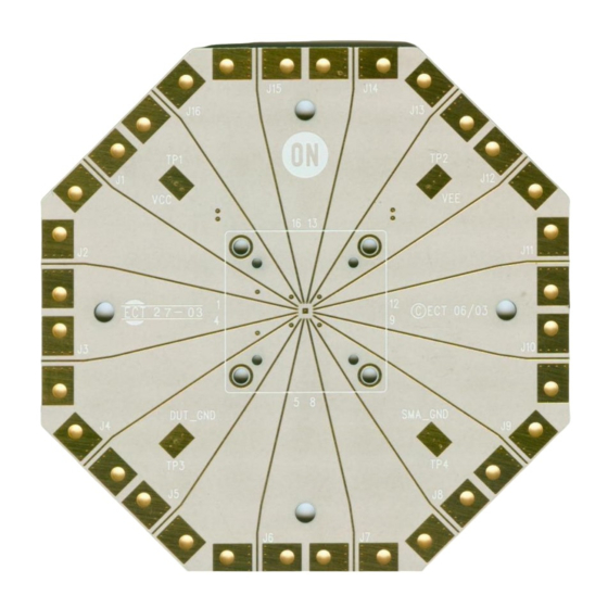
Top View
© Semiconductor Components Industries, LLC, 2013
October, 2021 − Rev. 1
can
be
ordered
from
Figure 1. Top and Bottom View of the 16 QFN Evaluation Board
EVAL BOARD USER'S MANUAL
Board Layout
The QFN16 Evaluation Board provides a high bandwidth,
50 W
controlled
impedance
implemented in four layers. The first layer or primary trace
layer is 0.008" thick Rogers RO4003 material, and is
designed to have equal electrical length on all signal traces
from the device under test (DUT) pins to the SMA
connectors. The second layer is the 1.0 oz copper ground
plane and is primarily dedicated for the SMA connector
ground plane. FR4 dielectric material is placed between the
second and third layers and between third and fourth layers.
The third layer is also 1.0 oz copper plane. A portion of this
layer is designated for the device V
planes. The fourth layer is the secondary trace layer.
1
www.onsemi.com
environment
and DUTGND power
CC
Bottom View
Publication Order Number:
EVBUM2183/D
and
is
Advertisement

Related Manuals for onsemi NB6L14MNG


Summary of Contents for onsemi NB6L14MNG
- Page 1 0.008″ thick Rogers RO4003 material, and is characterize and verify the operation of various onsemi designed to have equal electrical length on all signal traces products. Many QFN16EVBs are dedicated with a device...
-
Page 2: Silkscreen (Top Side)
LAYER 2 (GROUND PLANE P1) 1 OZ 0.062 ± 0.007 FR−4 0.020 in LAYER 3 (GROUND, VCC & VEE, PLANE P2) 1 OZ FR−4 0.025 in LAYER 4 (BOTTOM SIDE) 1 OZ Figure 4. Evaluation Board Layout, 4 Layer www.onsemi.com... - Page 3 If a device already installed, and can be ordered from internal resistors are provided, the VT pins should be wired onsemi.com at the specific device web page. to SMAGND. (More information on termination is provided Connecting Power and Ground in AND8020).
- Page 4 QFN16EVB, but it is not provided on the board, since there are several user dependent LVDS output measurement techniques. For LVDS lab setup and test, a single supply is typically used, ie. V = 3.3 V and DUTGND = 0 V. www.onsemi.com...
- Page 5 = Exposed Pad and must be tied to DUTGND/V CONFIGURATIONS VEE/DUTGND SMAGND DUTGND/V 13 14 15 16 ExPad Exposed Pad SMAGND Install 0.1 mF Decoupling Bottom View Capacitors here and at Top View package pins Figure 6. Power Supply Configuration for Device NB6L14M www.onsemi.com...
- Page 6 Supply Convertor “Spilt” Power Supply − − = 0 V SMAGND = 0 V DUTGND DUTGND DUTGND = −2.5 V or −3.3 V SMAGND +2.5 V Offset / “Split” Power Supply Configuration Figure 8. “Split” or Dual Power Supply Connections www.onsemi.com...
- Page 7 0603 0.1 mF ±10% 0603C104KAT2A Chip Resistor Panasonic* ERJ−2RKF49R9X http://www.panasonic.com 0402 50 W ±1% Precision Thick Film Chip Resistor Evaluation Board onsemi QFN 16 Evaluation Board QFN16EVB http://www.onsemi.com Device Samples onsemi QFN 16 Package Device NB6L14MMNG http://www.onsemi.com *Components are available through most distributors, i.e.
- Page 8 NB6L14MNGEVB Top Layer Second Layer (SMA_GND Plane) Figure 9. Gerber Files www.onsemi.com...
- Page 9 NB6L14MNGEVB Third Layer (DUT_GND Trace) Bottom Layer Figure 10. Gerber Files www.onsemi.com...
- Page 10 LIMITATIONS OF LIABILITY: onsemi shall not be liable for any special, consequential, incidental, indirect or punitive damages, including, but not limited to the costs of requalification, delay, loss of profits or goodwill, arising out of or in connection with the board, even if onsemi is advised of the possibility of such damages. In no event shall onsemi’s aggregate liability from any obligation arising out of or in connection with the board, under any theory of liability, exceed the purchase price paid for the board, if any.