Advertisement
Quick Links
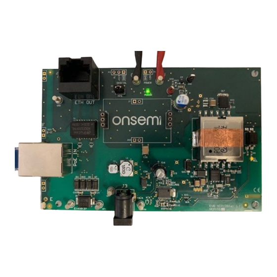
NCP1081 Evaluation Board
User's Manual
PoE−PD Interface & Flyback Controller
Board
NCP1081REF12VC4GEVB
General
The NCP1081REF12VC4GEVB board allows easy
implementation and evaluation of a Power−over−Ethernet
powered equipment that is able to operate with an assigned
power level up to 25.5 W. The evaluation board is based on
PoE Powered Device controller NCP1081 (U2) with
integrated PoE PD interface controller and Flyback DC/DC
controller. The Flyback converter on this NCP1081 based
reference design generates a 12 V output voltage that is
isolated from the Ethernet link conductors.
Figure 1. Operational NCP1081REF12VC4GEVB
showing Basic Interconnections
The NCP1081REF12VC4GEVB board is designed as a
PoE splitter: having a PoE−enabled Ethernet port (labeled
"PoE IN") as input and generating an isolated 12 V supply
while passing through the data to another Ethernet port
(labeled "ETH OUT").
© Semiconductor Components Industries, LLC, 2022
November, 2022 − Rev. 0
EVAL BOARD USER'S MANUAL
Quick Start Guide
Step 1: Make sure the jumper is mounted on header P3
(labeled "MPS").
Step 2: Insert the Ethernet cable (cf. blue cable in the picture
on the left) coming from the PSE in the Ethernet connector
J2 labeled "PoE IN".
Step 3: Observe the status LEDs.
If the PSE powers up the system, the green POWER−ON
LED (labeled "PWRON") should be ON.
The status of the yellow LED (labeled "NCL") depends on
the PSE being used.
Step 4: Optionally connect the turret terminals that are
labeled "GND" and "12V" to a DC electronic load (cf. black
and red clips in the picture on the left). The DC electronic
load behind the NCP1081 EVB should be operational over
a 11 V to 13 V voltage range.
1
www.onsemi.com
Publication Order Number:
EVBUM2849/D
Advertisement

Related Manuals for onsemi NCP1081


Summary of Contents for onsemi NCP1081
- Page 1 “GND” and “12V” to a DC electronic load (cf. black and red clips in the picture on the left). The DC electronic load behind the NCP1081 EVB should be operational over a 11 V to 13 V voltage range.
- Page 2 Class or power level is preferred, resistor R26 NCP1081REF12VC4GEVB remains powered. This load labeled “CLASS” should be changed. See the NCP1081 resistor R15 is enabled when a jumper is placed on header datasheet for the nominal resistance values.
- Page 3 Figure 2. Output Current vs. PoE Input Voltage – Full Input Power Load (Class 4) Figure 3. Output Current vs. PoE Input Voltage – Full Input Power Load (Class 3) Figure 4. PoE Input Current vs PoE Input Voltage – No Output Load except R15 www.onsemi.com...
- Page 4 NCP1081REF12VC4GEVB Figure 5. Efficiency vs. Output Current Figure 6. Efficiency vs. Output Current − Zoom In www.onsemi.com...
- Page 5 NCP1081REF12VC4GEVB Figure 7. Efficiency vs. Output Current − from (VPP,RTN) to (12V,GND) www.onsemi.com...
- Page 6 NCP1081REF12VC4GEVB Figure 8. 12 V Output Ripple and Noise Figure 9. V Primary Mosfet Q2 (V = 57 V) DrainSource Figure 10. V Secondary Diode D17 (V = 57 V) CathodeAnode www.onsemi.com...
- Page 7 NCP1081REF12VC4GEVB Figure 11. Thermal Image − Top Figure 12. Thermal Image − Bottom www.onsemi.com...
- Page 8 NCP1081REF12VC4GEVB Figure 13. Emission Test DUT: NCP1081REF12VGEVB with 7.3 W Load www.onsemi.com...
- Page 9 Table 3. CONDUCTED EMISSION − FINAL RESULT CAV Frequency (MHz) CAverage (dBmV) Limit (dBmV) Margin (dB) Corr. (dB) 7.503000 58.25 64.00 5.76 8.038500 59.12 64.00 4.88 8.844000 59.30 64.00 4.70 9.379500 60.29 64.00 3.71 9.915000 57.94 64.00 6.06 10.047750 58.08 64.00 5.92 www.onsemi.com...
- Page 10 (cm) (deg) (dB/m) 31.160000 28.15 40.00 11.85 1000.0 120.000 98.0 173.0 −9.9 31.180000 26.45 40.00 13.55 1000.0 120.000 122.0 253.0 −9.9 34.360000 27.29 40.00 12.71 1000.0 120.000 103.0 138.0 −11.8 34.900000 29.86 40.00 10.14 1000.0 120.000 98.0 309.0 −12.1 www.onsemi.com...
- Page 11 NCP1081REF12VC4GEVB Figure 16. Schematic Diagram NCP1081REF12VC4GEVB www.onsemi.com...
-
Page 12: Additional Information
LIMITATIONS OF LIABILITY: onsemi shall not be liable for any special, consequential, incidental, indirect or punitive damages, including, but not limited to the costs of requalification, delay, loss of profits or goodwill, arising out of or in connection with the board, even if onsemi is advised of the possibility of such damages. In no event shall onsemi’s aggregate liability from any obligation arising out of or in connection with the board, under any theory of liability, exceed the purchase price paid for the board, if any.
Need help?
Do you have a question about the NCP1081 and is the answer not in the manual?
Questions and answers