Table of Contents
Advertisement
Quick Links
NB7NPQ1102MCMUGEVB Evaluation Board User's
Manual
NB7NPQ1102MCMUGEVB
Introduction
The NB7NPQ1102MCMUGEVB evaluation board was
developed to provide a convenient platform to quickly
verify the operation of the NB7NPQ1102M redriver in a
USB type−C system environment.
This evaluation board manual contains:
•
Information on the NB7NPQ1102M Evaluation Board
•
Board Schematics
•
Board Features
•
Accommodates the Functional Evaluation of the
NB7NPQ1102M
•
Acts as a Reference Design that Can Easily be
Modified for Active Cables, UFP (Upstream Facing
Port), DFP (Downstream Facing Port), and DRP (Dual
Role Port) Applications
•
Type−C Plug and Receptacle to Easily Place in the
Existing System Environment
•
On Board Control Pins for Adjusting Settings without
Compromising Form Factor
•
Two NB7NPQ1102M Devices to Facilitate USB
Type−C Connections without using a Multiplexor
Part Description
The NB7NPQ1102M is a 3.3 V dual channel, high gain,
redriver for USB 3.1 Gen 1 and USB 3.1 Gen 2 applications
that supports both 5 Gbps and 10 Gbps data rates. Signal
integrity degrades from PCB traces, transmission cables,
and inter−symbol interference (ISI). The NB7NPQ1102M
compensates for these losses by engaging varying levels of
equalization at the input receiver, and flat gain amplification
on the output transmitter. The Flat Gain and Equalization are
controlled by four level control pins. Each channel has a set
of independent control pins to make signal optimization
possible.
After power up, periodic check of TX output is made for
the receiver connection. When the receiver is detected, the
RX termination becomes enabled and the device is set to
perform the redriver function. Note that both the channels
are independent of each other. The flexibility of this part
allows it to fit into many system applications
The NB7NPQ1102M comes in a small 3 x 3 mm UQFN16
package and is specified to operate across the entire
industrial temperature range of –40°C to 85°C.
© Semiconductor Components Industries, LLC, 2022
February, 2022 − Rev. 0
EVAL BOARD USER'S MANUAL
This manual should be used in conjunction with the device
datasheet which contains full technical details on the device
specifications and operation.
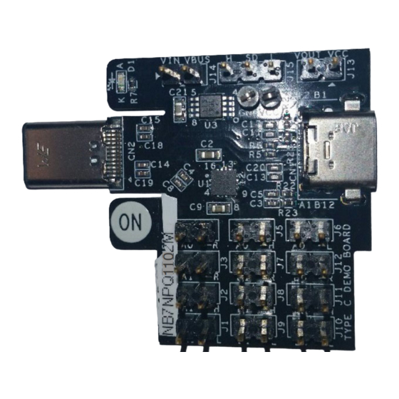
Figure 1. Kit Contents
1
www.onsemi.com
Publication Order Number:
EVBUM2655/D
Advertisement
Table of Contents

Subscribe to Our Youtube Channel
Related Manuals for onsemi NB7NPQ1102MCMUGEVB


Summary of Contents for onsemi NB7NPQ1102MCMUGEVB
- Page 1 NB7NPQ1102MCMUGEVB Evaluation Board User's Manual NB7NPQ1102MCMUGEVB Introduction The NB7NPQ1102MCMUGEVB evaluation board was This manual should be used in conjunction with the device developed to provide a convenient platform to quickly datasheet which contains full technical details on the device verify the operation of the NB7NPQ1102M redriver in a specifications and operation.
- Page 2 NB7NPQ1102MCMUGEVB BOARD MAP AND FUNCTIONAL SUMMARY Jumper J15: This Jumper Jumper J13: This Jumper J14: This pulls Enable Pin to Jumper connects the Jumper connects the different Voltage levels. 3.3V LDO Output to 5V USB Bus to the This Pin should be kept the two VCC of the input of 3.3V LDO...
- Page 3 Figure 3. NB7NPQ1102M Evaluation Board − Connecting to an External Power Supply Select Power Source useful if you cannot easily tell whether the downstream The NB7NPQ1102MCMUGEVB has the flexibility to be facing port has acknowledged a super speed (+) connection powered through USB’s VBUS, or an external power with the inserted loss, or if it stepped down to high speed data supply.
- Page 4 NB7NPQ1102MCMUGEVB VBUS GND Via VCC Clip GND Clip Enable Output Input 3.3V Figure 4. Power Source Selection Table 1. SELECTING A POWER SOURCE USB VBUS Place jumper on J14 and a Jumper on J13 External Supply Open J14 and connect positive lead of external supply to VCC clip and apply 3.3 V. Ensure that GND clip is connected to ground and that current limit is set to 300 mA.
- Page 5 NB7NPQ1102MCMUGEVB COMPLETE BOARD SCHEMATICS NB7NPQ1102M NB7NPQ1102M Figure 5. NB7NPQ1102M USB Type−C Evaluation Board Schematics www.onsemi.com...
- Page 6 NB7NPQ1102MCMUGEVB BILL OF MATERIAL Table 2. BILL OF MATERIALS Description Schematic Reference Manufacturer Manufacturer Part Number 3.3 V Dual Channel USB3.1 U1, U2 onsemi NB7NPQ1102MMUTXG High Gain Linear Re−driver Header, 0.100” J1; J2; J3; J4; J5; J6; J7; J8; J9;...
- Page 7 LIMITATIONS OF LIABILITY: onsemi shall not be liable for any special, consequential, incidental, indirect or punitive damages, including, but not limited to the costs of requalification, delay, loss of profits or goodwill, arising out of or in connection with the board, even if onsemi is advised of the possibility of such damages. In no event shall onsemi’s aggregate liability from any obligation arising out of or in connection with the board, under any theory of liability, exceed the purchase price paid for the board, if any.
Need help?
Do you have a question about the NB7NPQ1102MCMUGEVB and is the answer not in the manual?
Questions and answers