Table of Contents
Advertisement
Quick Links
Notice to End Users
This UserÕs Guide & Technical Reference is for assisting system
manufacturers and end users in setting up and installing the
mainboard.
Every effort has been made to ensure that the information in this
manual is accurate. Soltek Computer Inc. is not responsible for
printing or clerical errors. Information in this document is subject
to change without notice and does not represent a commitment on
the part of Soltek Computer Inc.
No part of this manual may be reproduced, transmitted, translated
into any language in any form or by any means, electronic or
mechanical, including photocopying and recording, for any purpose
without the express written permission of Soltek Computer Inc.
Companies and products mentioned in this manual are for
identification purposes only. Product names appearing in this
manual may or may not be registered trademarks or copyrights of
their respective companies.
S
C
I
.
OLTEK
OMPUTER
NC
PROVIDES THIS MANUAL
WITHOUT WARRANTY OF ANY KIND
INCLUDING BUT NOT LIMITED TO THE IMPLIED WARRANTIES OR
CONDITIONS OF MERCHANTABILITY OR FITNESS FOR A
. I
PARTICULAR PURPOSE
N NO EVENT SHALL
I
.
NC
BE LIABLE FOR ANY LOSS OR PROFITS
,
OF USE OR DATA
INTERRUPTION OF BUSINESS
,
,
SPECIAL
INCIDENTAL
OR CONSEQUENTIAL DAMAGES OF ANY
,
S
C
KIND
EVEN IF
OLTEK
OMPUTER
POSSIBILITY OF SUCH DAMAGES ARISING FROM ANY DEFECT OR
ERROR IN THIS MANUAL OR PRODUCT
© Copyright 1997 Soltek Computer Inc. All right reserved
For more information, please visit http://www.soltek.com.tw
Edition: January 1997
Version: 2.0
SL-54A2/A5 SERIAL
Ò
Ó
AS IS
,
,
EITHER EXPRESS OR IMPLIED
S
C
OLTEK
OMPUTER
,
,
LOSS OF BUSINESS
LOSS
,
,
OR FOR INDIRECT
I
.
NC
HAS BEEN ADVISED OF THE
.
i
Advertisement
Table of Contents

Related Manuals for SOLTEK SL-54A2


Summary of Contents for SOLTEK SL-54A2
- Page 1 Every effort has been made to ensure that the information in this manual is accurate. Soltek Computer Inc. is not responsible for printing or clerical errors. Information in this document is subject to change without notice and does not represent a commitment on the part of Soltek Computer Inc.
-
Page 3: Table Of Contents
Contents Chapter 1: Introduction --------------------------------------- 1 Features ------------------------------------------------------------------------- 1 CPU ------------------------------------------------------------------------ 1 Chipset -------------------------------------------------------------------- 1 L2 Cache ------------------------------------------------------------------ 1 Main Memory ----------------------------------------------------------- 1 BIOS ------------------------------------------------------------------------ 2 Giga I/O Function ------------------------------------------------------ 2 Other Functions --------------------------------------------------------- 2 Mainboard Setting for Pentium MMX-166----------------------------- 3 Chapter 2: Hardware Setup ---------------------------------- 4 INTEL Pentium MMX CPUs Settings ----------------------------------- 4 Intel Pentium MMXÐ166/200/233 (Red Caps) ------------------ 4... - Page 4 CPU 2.0X Clock Setting (Red Caps) -------------------------------- 8 Intel Pentium Ð 120/133 CPUs --------------------------------- 8 CPU 2.5X Clock Setting (Red Caps) -------------------------------- 9 Intel Pentium Ð 150/166 CPUs --------------------------------- 9 CPU 3.0X Clock Setting (Red Caps) -------------------------------- 9 Intel Pentium Ð 180/200 CPUs --------------------------------- 9 Cyrix 6x86 CPUs ----------------------------------------------------------- 10 CPU 2.0X Clock Setting (Red Caps) ------------------------------ 10 Cyrix 6x86 Ð...
- Page 5 IDE1/IDE2: Primary/Secondary IDE Connectors----------- 20 Power Connector ----------------------------------------------------- 21 IDE LED Activity Light: (J1 pin1Ð4)------------------------------ 22 Infrared Port Module Connector (J1 pin6Ð10) ----------------- 22 J1 pin12, 13: Reserved ----------------------------------------------- 22 SMI Switch (J1 pin14, 15)-------------------------------------------- 22 Speaker Connector (J2 pin1Ð4) ------------------------------------ 22 Reset Switch (J2 pin5, 6)--------------------------------------------- 22 Power LED and Keylock Switch (J2 pin8Ð12)------------------ 22 Turbo LED (J2 pin14, 15)-------------------------------------------- 23...
-
Page 7: Chapter 1: Introduction
Chapter 1 Introduction Features 1. Supports Intel Pentium P54C/MMX (P55C) CPUs at 75 ~ 233 MHz 2. Supports Cyrix 6x86(L) CPUs at PR120 + ~ PR166 + MHz (PR200 + MHz is optional) 3. Supports AMD K5, K6 CPUs at PR75 ~ PR233 4. -
Page 8: Bios
BIOS 1. AWARD Plug and Play BIOS 2. Supports Advanced Power Management Function 3. Flash Memory for easy upgrade Giga I/O Function 1. Integrated USB (Universal Serial Bus) controller with two USB ports. 2. Supports 2 IDE channels with 4IDE devices (including 120MB IDE floppy) 3. -
Page 9: Mainboard Setting For Pentium Mmx-166
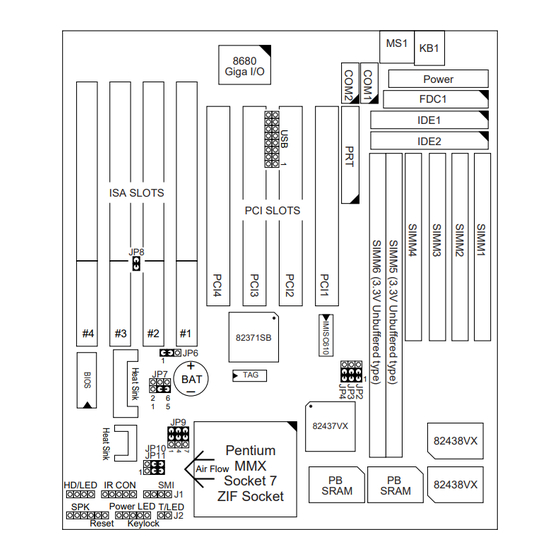
Mainboard Setting for Pentium MMX-166 The settings of the following figure is for the Pentium MMX- 166 with the 256K cache. To get the best cooling effect, make sure that the airflow from the CPU fan is facing the heatsink. (MMX is dual voltage CPU, do not use this setting if CPU is not MMX or 6x86L.) 8680... -
Page 10: Chapter 2: Hardware Setup
Chapter 2 Hardware Setup INTEL Pentium MMX CPUs Settings Intel Pentium MMX–166/200/233 JP10 JP11 Pentium Pentium MMX–166/66 Pentium MMX–200/66 Pentium MMX–233/66 JP10 JP10 JP10 JP11 JP11 JP11 Figure 2Ð1. CPU Type Configuration Note: INTEL Pentium MMX (P55C) is a dual voltage CPU. JP7 and JP9 must be set correctly (refer to page 12). -
Page 11: Amd K6 Cpu Settings
AMD K6 CPU Settings AMD K6 – PR166/200/233 JP10 JP11 AMD K6–PR166/66 AMD K6–PR200/66 AMD K6–PR233/66 JP10 JP10 JP10 JP11 JP11 JP11 Figure 2Ð2. CPU Type Configuration Note: AMD K6 is a dual voltage CPU. JP7 and JP9 must be set correctly (refer to page 12). -
Page 12: Cyrix M2 Settings (Pending)
Cyrix M2 Settings (Pending) Cyrix M2 – PR166/200/233 JP10 JP11 Cyrix Pending Pending Pending Figure 2Ð3. CPU Type Configuration (Pending) Note: Cyrix M2 is a dual voltage CPU. JP7 and JP9 must be set correctly (refer to page 12). Check with your CPU supplier for CPU voltage specification. -
Page 13: Cyrix 6X86L Cpus Setting (Red Caps)
Cyrix 6x86L CPUs Setting Cyrix 6x86L – PR120 + /PR133 + /PR150 + /PR166 + /PR200 + CPUs Cyrix 6x86L – PR120 + /50 Cyrix 6x86L – PR133 + /55 Cyrix 6x86L – PR150 + /60 Pentium – 120/60 JP10 JP11 Cyrix 6x86L –... -
Page 14: Intel Pentium Cpus
Intel Pentium CPUs CPU 1.5X Clock Setting (Red Caps) Intel Pentium – 75/90/100 CPUs Pentium – 75/50 Pentium – 90/60 JP10 JP11 Pentium Pentium – 100/66 Figure 2Ð5. CPU Type Configuration CPU 2.0X Clock Setting (Red Caps) Intel Pentium – 120/133 CPUs Pentium –... -
Page 15: Cpu 2.5X Clock Setting (Red Caps)
CPU 2.5X Clock Setting (Red Caps) Intel Pentium – 150/166 CPUs Pentium – 150/60 Pentium – 166/66 Pentium JP10 JP11 Figure 2Ð7. CPU Type Configuration CPU 3.0X Clock Setting (Red Caps) Intel Pentium – 180/200 CPUs Pentium – 180/60 Pentium – 200/66 Pentium JP10 JP11... -
Page 16: Cyrix 6X86 Cpus
Cyrix 6x86 CPUs CPU 2.0X Clock Setting (Red Caps) Cyrix 6x86 – PR120 + /PR133 + /PR150 + /PR166 + /PR200 + CPUs Cyrix 6x86– PR120 + /50 Cyrix 6x86 – PR133 + /55 Cyrix 6x86 – PR150 + /60 Pentium –... -
Page 17: Amd Cpus
AMD CPUs AMD K5 – PR75/PR90/PR100/PR120/PR133 CPUs (Red Caps) K5 – PR75/50 K5–PR90/60 (ID=0x50) K5–PR120/60 (ID=0x51) JP10 AMD K5 JP11 K5–PR100/66 (ID=0x50) 1.5x clock K5–PR133/66 (ID=0x51) Figure 2Ð10. CPU Type Configuration AMD K5 – PR150/PR166 CPUs (Red Caps) K5 – PR150/60 K5 –... -
Page 18: Cpu Voltage Setting
CPU Voltage Setting Single Voltage Settings (Green Caps) For Intel Pentium P54C Family, Cyrix 6x86 Family, AMD K5 (PR75 ~ PR166) Family 3.38V CPU Pentium 3.52V CPU Dual Voltage Settings (Green Caps) For Intel Pentium MMX (P55C) Family, Cyrix 6x86L/M2 Family, AMD K6 Family = 3.38V = 2.8V... -
Page 19: System Memory Configuration
System Memory Configuration This 82430VX motherboard supports 72-pin SIMMs of 4MB, 8MB, 16MB, or 32MB to form a memory size between 8MB to 128MB. Follow the chart below to install the memory modules. Bank 0 Bank 1 SIMM 3 & 4 or 6 SIMM 1 &... -
Page 20: Jumper Settings
Jumper Settings JP10, JP11: Bus Ratio Select Set these jumpers according to your CPU clock. JP10 Ratio JP11 1.5X (default) 2.5X Notice that the color of the cap is RED. – JP10 JP11 JP10 JP11... -
Page 21: Jp6: Clear Cmos Data
JP6: Clear CMOS Data Clear the CMOS memory by shorting this jumper momentarily; then remove the cap to retain new settings. COMS Data Clear Data Retain Data (default) – Hardware Installation 15... -
Page 22: Jp8: Isa Clock Select
JP8: ISA Clock Select This jumper sets the ISA clock of different CPUs. ISA Clock PCI Clock/3 Open (for Bus Clock = 50 MHz CPU) PCI Clock/4 Close (default) (for Bus clock = 60/66 MHz CPU) – Note: 1. ISA clock is controlled when the BIOS finishes chipset initial. -
Page 23: Jp2, Jp3, Jp4: External Bus Frequency Select
JP2, JP3, JP4: External Bus Frequency Select These 3 jumpers tells the clock generator what frequency to send to the CPU. Set these jumpers as shown, according to the CPUÕs internal clock speed. Settings Settings 50MHz 66MHz (default) 55MHz 75MHz 60MHz Notice that the color of the cap is RED. -
Page 24: Connectors
Connectors KB1: Keyboard Connector A 5-pin female DIN keyboard connector is located at the upper right corner of the motherboard. Plug the keyboard jack direct to this connector. MS1: PS/2 Mouse Connector Attach PS/2 mouse cable to this 6-pin connector. Keyboard Connector PS/2 Mouse Connector... -
Page 25: Prt: Parallel Port
PRT: Parallel Port The system board provides a 2x13-pin parallel port connector, PRT. Attach parallel port cable to this connector. COM1 /COM2: Serial Port Connectors The system board has two 2x5-pin serial port connectors, COM1 and COM2. Attach COM1/COM2 cables to these connectors. -
Page 26: Fdc: Floppy Drive Connector
FDC: Floppy Drive Connector The system board has a 2x17-pin floppy drive connector, FDC. Connect one end of a floppy drive cable to this connector and the other end to a floppy drive. IDE1/IDE2: Primary/Secondary IDE Connectors The system board has a 32-bit Enhanced PCI IDE Controller that provides for two HDD connectors, IDE1 (primary) and IDE2 (secondary). -
Page 27: Power Connector
Power Connector The power connector has two 6-pin male header connectors. Plug the dual connectors from the power directly onto the board connector while making sure the black leads are in the center. Power Connector – Hardware Installation 21... -
Page 28: Ide Led Activity Light: (J1 Pin1Ð4)
IDE LED Activity Light: (J1 pin1–4) This connector connects to the hard disk activity indicator light on the case. Infrared Port Module Connector (J1 pin6–10) The system board provides a 5-pin infrared connectorÑIR1 as an optional module for wireless transmitting and receiving. -
Page 29: Turbo Led (J2 Pin14, 15)
Turbo LED (J2 pin14, 15) Connect the caseÕs turbo LED to this connector. – HD/LED IR CON HD/LED IR CON Power LED T/LED Power LED T/LED Reset Keylock Reset Keylock HD/LED IR CON 9 10 12 13 14 15 9 10 11 12 14 15 Power Turbo... -
Page 30: Usb1: Usb Connector
USB1: USB Connector This jumper connects to the USB cable to provide USB device. – D0– D1–... -
Page 31: J1 Switch Signal Summary
J1 Switch Signal Summary Signal Description HDD LED Connector HDD LED Signal HDD LED Signal N.C. No Connection Infrared Transmit Signal Infrared Connector Infrared Receive Signal (low speed) Infrared Receive Signal (high speed) N.C. No Connection N.C. No Connection SMI Signal Hardware Installation 25... -
Page 32: J2 Switch Signal Summary
J2 Switch Signal Summary Signal Description Speaker Signal Speaker Connector No Connection Ground Reset Switch Reset Signal Ground N.C. No Connection Power LED Connector No Connection Ground Keylock Connector Keylock Signal N.C. No Connection Turbo LED Connector Turbo LED Connector Ground Power Connector Description... -
Page 33: Chapter 3: Award Bios Setup
Chapter 3 Award BIOS Setup This 82430VX motherboard comes with the AWARD BIOS from AWARD Software Inc. Enter the Award BIOS programÕs Main Menu as follows: 1. Turn on or reboot the system. After a series of diagnostic checks, the following message will appear: PRESS <DEL>... -
Page 34: Standard Cmos Setup
3. Using one of the arrows on your keyboard to select an option and press <Enter>. Modify the system parameters to reflect the options installed in the system. 4. You may return to the Main Menu anytime by press <ESC> . 5. - Page 35 A short description of screen options follows: Date (mm:dd:yy) Set the current date and time. Time (hh:mm:ss) This field records the specifications Primary (Secondary) for all non-SCSI hard disk drives Master/Slave installed in your system. Refer to the respective documentation on how to install the drivers.
-
Page 36: Bios Features Setup
BIOS Features Setup BIOS Features Setup allows you to improve your system performance or set up some system features according to your preference. Run the BIOS Features Setup as follows: 1. Choose ÒBIOS FEATURES SETUPÓ from the Main Menu and a screen with a list of options appears. ROM PCI/ISA BIOS BIOS FEATURES SETUP AWARD SOFTWARE, INC. - Page 37 A short description of screen options follows: CPU Internal Choose Enabled (default) or Cache Disabled. This option allows you to enable or disable the CPUÕs internal cache. External Cache Choose Enabled (default) or Disabled. This option allows you to enable or disable the external cache memory.
- Page 38 Gate A20 Option Choose Normal or Fast (default). This option allows the RAM to access the memory above 1MB by using the fast gate A20 line. Typematic Rate Choose Enabled or Disabled Setting (default). Enable this option to adjust the keystroke repeat rate. Typematic Rate Range between 6 (default) and 30 (Chars/Sec)
-
Page 39: Chipset Features Setup
Chipset Features Setup Chipset Features Setup changes the values of the chipset registers. These registers control the system options. Run the Chipset Features Setup as follows: 1. Choose ÒCHIPSET FEATURES SETUPÓ from the Main Menu and a screen with a list of options appears. ROM PCI/ISA BIOS CHIPSET FEATURES SETUP AWARD SOFTWARE, INC. - Page 40 DRAM RAS# Use the default setting. This option allows you to determine the number Precharge Time of the CPU clocks allocated for the RAS to accumulate/charge it before the DRAM is refreshed. DRAM R/W Use the default setting. This sets the Leadoff Timing point of time that the CPU is allowed to read and write to DRAM...
- Page 41 ISA Bus Clock Default is PCICLK/4. The best value is as close to 8MHz as possible. System BIOS Choose Enabled or Disabled Cacheable (default). When Enabled, the access to the system BIOS ROM addressed at F0000H-FFFFFH is cached. Video BIOS Choose Enabled or Disabled Cacheable (default).
-
Page 42: Power Management Setup
Chipset NA# Enabled (default) : Enable CPU pipeline function. Asserted Disabled: Disable CPU pipeline function. 3. Press <ESC> and follow the screen instructions to save or disregard your settings. Power Management Setup Power Management Setup sets the systemÕs power saving functions. - Page 43 A short description of screen options follows: Power Choose Max. Saving, User Define, Management Disabled (default), or Min Saving. Choose Yes or No (default). You PM Control by need to choose Yes when the operating system has the APM functions, choose No otherwise. Video Off Method Choose Blank , DPMS, or V/H Sync+Blank (default).
-
Page 44: Pnp/Pci Configuration Setup
HDD power Down Time is adjustable from 1 to 15 minutes. When the set time has elapsed, the BIOS sends a command to the HDD to power down, which turns off the motor. IRQx (Wake-Up Set these IRQs individually. Event) Activity detected from any enabled IRQ channel (ON) will wake up the system. - Page 45 A short description of screen options follows: Resources Choose Manual (default) or Auto. Controlled By The BIOS checks the IRQ/DMA channel number on the ISA and PCI card manually if chose Manual and the IRQ/DMA channel number will be checked automatically if choose Auto.
-
Page 46: Load Setup Defaults
Used MEM Choose 8K, 16K, 32K, or 64K. Length* With the above two functions, users can define where the used memory address is located and its corresponding length of the legacy area. BIOS will skip the UMB area which is used by the legacy device to avoid memory space conflict. -
Page 47: Integrated Peripherals
Integrated Peripherals Integrated Peripherals option changes the values of the chipset registers. These registers control system options in the computer. 1. Choose ÒINTEGRATED PERIPHERALSÓ from the Main Menu and a screen with a list of options appears. ROM PCI/ISA BIOS INTEGRATED PERIPHERALS AWARD SOFTWARE, INC. - Page 48 IDE Primary Choose Auto (default) or Mode 0~4. The BIOS will detect the HDD Mode Master/Slave PIO IDE Secondary type automatically when you Master/Slave PIO choose Auto. You need to set to a lower mode than Auto when your hard disk becomes unstable. On-Chip Primary/ Enabled (default): Turn on the Secondary PCI IDE...
- Page 49 Onboard Serial Choose Auto (default), 3F8/IRQ4 , 2F8/IRQ3, 3E8/IRQ4, 2E8/IRQ3, or Port 2 Disabled. UR2 Mode Choose Standard (default), IrDA1.0, ASKIR, MIR 0.57M, MIR 1.15M, or FIR. UR2 Duplex Choose Half (default), or Full. Mode* Half: DoesnÕt transmit and receive activities at the same time.
-
Page 50: Supervisor/User Password
Supervisor/User Password These two options allows you to set your system passwords. Normally, supervisor has a higher right to change the CMOS setup option than the user. The way to set up the passwords for both Supervisor and User are as follow: 1. -
Page 51: Ide Hdd Auto Detection
IDE HDD Auto Detection IDE HDD Auto Detection detects the parameters of an IDE hard disk drive and automatically enters them to the Standard CMOS Setup screen. The screen will ask you to select a specific hard disk for Primary Master after you select this option. If you accept a hard disk detected by the BIOS, you can enter ÒYÓ...
Need help?
Do you have a question about the SL-54A2 and is the answer not in the manual?
Questions and answers