Table of Contents
Advertisement
Quick Links
Notice to End Users
This UserÕs Guide & Technical Reference is for assisting system
manufacturers and end users in setting up and installing the
mainboard.
Every effort has been made to ensure that the information in this
manual is accurate. Soltek Computer Inc. is not responsible for
printing or clerical errors. Information in this document is subject
to change without notice and does not represent a commitment on
the part of Soltek Computer Inc.
No part of this manual may be reproduced, transmitted, translated
into any language in any form or by any means, electronic or
mechanical, including photocopying and recording, for any purpose
without the express written permission of Soltek Computer Inc.
Companies and products mentioned in this manual are for
identification purposes only. Product names appearing in this
manual may or may not be registered trademarks or copyrights of
their respective companies.
S
C
I
.
OLTEK
OMPUTER
NC
PROVIDES THIS MANUAL
WITHOUT WARRANTY OF ANY KIND
INCLUDING BUT NOT LIMITED TO THE IMPLIED WARRANTIES OR
CONDITIONS OF MERCHANTABILITY OR FITNESS FOR A
. I
PARTICULAR PURPOSE
N NO EVENT SHALL
I
.
NC
BE LIABLE FOR ANY LOSS OR PROFITS
,
OF USE OR DATA
INTERRUPTION OF BUSINESS
,
,
SPECIAL
INCIDENTAL
OR CONSEQUENTIAL DAMAGES OF ANY
,
S
C
KIND
EVEN IF
OLTEK
OMPUTER
POSSIBILITY OF SUCH DAMAGES ARISING FROM ANY DEFECT OR
ERROR IN THIS MANUAL OR PRODUCT
© Copyright 1998 Soltek Computer Inc. All right reserved
Web site: http://www.soltek.com.tw
email:
support@mail.soltek.com.tw
Edition: January 1998
Version: 1.0
SL–55B5 SERIAL
ii
Ò
Ó
AS IS
,
,
EITHER EXPRESS OR IMPLIED
S
C
OLTEK
OMPUTER
,
,
LOSS OF BUSINESS
LOSS
,
,
OR FOR INDIRECT
I
.
NC
HAS BEEN ADVISED OF THE
.
Advertisement
Table of Contents

Related Manuals for SOLTEK SL-55B5


Summary of Contents for SOLTEK SL-55B5
- Page 1 Every effort has been made to ensure that the information in this manual is accurate. Soltek Computer Inc. is not responsible for printing or clerical errors. Information in this document is subject to change without notice and does not represent a commitment on the part of Soltek Computer Inc.
- Page 2 Contents iii...
-
Page 3: Table Of Contents
Contents Chapter 1: Introduction --------------------------------------- 1 Features ------------------------------------------------------------------------- 1 CPU ------------------------------------------------------------------------ 1 Chipset -------------------------------------------------------------------- 1 L2 Cache ------------------------------------------------------------------ 1 Main Memory ----------------------------------------------------------- 1 BIOS ------------------------------------------------------------------------ 3 I/O Function ------------------------------------------------------------- 3 Other Functions --------------------------------------------------------- 3 Mainboard Setting for Pentium MMX-166----------------------------- 4 Chapter 2: Hardware Setup ---------------------------------- 5 CPU VCORE Voltage Setting---------------------------------------------- 5 JP1: CPU VCore Voltage Setting ----------------------------------- 5... - Page 4 Infrared Port Module Connector (J1 pin6Ð10) ----------------- 14 J1 pin12, 13: ATX Power Button ---------------------------------- 14 J1 pin14, 15: Reserved ----------------------------------------------- 14 Speaker Connector (J2 pin1Ð4) ------------------------------------ 15 Reset Switch (J2 pin5, 6)--------------------------------------------- 15 Power LED and Keylock Switch (J2 pin8Ð12)------------------ 15 Turbo LED (J2 pin14, 15)-------------------------------------------- 16 J1 Switch Signal Summary ----------------------------------------- 17 J2 Switch Signal Summary ----------------------------------------- 18...
-
Page 6: Chapter 1: Introduction
Chapter 1 Introduction Features 1. Supports Intel Pentium P54C/MMX (P55C) CPUs at 90 ~ 233 MHz; 2. Supports Cyrix 6x86(L) CPUs at PR133 + ~ PR200 + MHz and 6x86MX (M2) CPUs at PR166 + ~ PR266 +; 3. Supports AMD K5: PR90 ~ PR200 and AMD K6: 166 ~ 366;... -
Page 7: Bios
3. Supports 2pcs 72pin SIMM sockets and 3 pcs of 168pin DIMM sockets (3.3V unbuffered type). BIOS 1. AWARD Plug and Play BIOS; 2. Supports Advanced Power Management Function; 3. Flash Memory for easy upgrade. I/O Function 1. Integrated USB (Universal Serial Bus) controller with two USB ports;... -
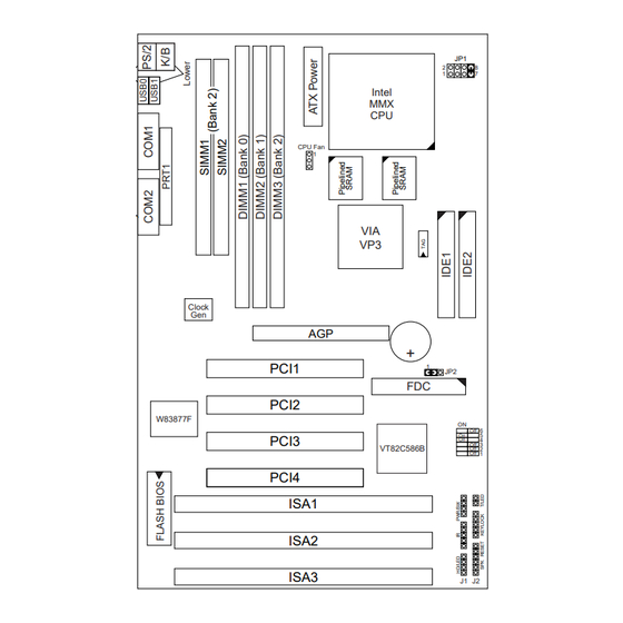
Page 8: Mainboard Setting For Pentium Mmx-166
Mainboard Setting for Pentium MMX-166 The default settings of the following figure is for the INTEL Pentium MMX-166 with the 512K (or 256K) cache. Intel CPU Fan Clock PCI1 PCI2 W83877F PCI3 VT82C586B PCI4 ISA1 ISA2 ISA3 J1 J2 Figure 1–1. SL–55B5 Motherboard Layout Introduction 3... -
Page 9: Chapter 2: Hardware Setup
Chapter 2 Hardware Setup CPU V Voltage Setting CORE JP1: CPU V Voltage Setting Core Core Core Core Core JP13 Voltage Voltage Voltage Voltage 3.2V* 2.8V 2.0V 2.4V K6Ð233 MMX, 6x86L (or higher) 3.3V 2.9V 2.1V* 2.5V IDT C6 K6Ð166/200 6x86MX (M2) 2.2V 2.6V... -
Page 10: Agp Driver For Win95 Installation
Note: 1. Refer to the table above to choose the correct voltage for the CPU everytime that you install a CPU. 2. Make sure that your JP1 is matched with the CPU voltage, otherwise will damage the CPU or make the system unstable. 3. -
Page 11: Intel Pentium Mmxð166/200/233 Cpus
Follow the below procedure to check if the AGP driver is capable to activate: 1. Activate ÒControl Panel,Ó 2. Click ÒDirectX,Ó 3. Click ÒDirectDraw,Ó and 4. Check if there are some values in ÒBitÓ and ÒOverlays.Ó If there are some values, the AGP is able to activate. Intel Pentium MMX–166/200/233 CPUs Intel (2.8V) -
Page 12: Amd K6 Cpu Settings
AMD K6 CPU Settings AMD K6 – 166/200/233 CPUs (2.9V) (3.2V) K6–166 K6–200 K6–233 1 2 3 4 5 6 1 2 3 4 5 6 1 2 3 4 5 6 Figure 2–2. CPU Type Configuration Note: 1. K6–166 and K6–200 are 2.9V CPUs. 2. -
Page 13: Amd K6 Ð 266/300/333/366 Cpus
AMD K6 – 266/300/333/366 CPUs (2.2V) K6–266 K6–300 K6–333 K6–366 1 2 3 4 5 6 1 2 3 4 5 6 1 2 3 4 5 6 1 2 3 4 5 6 Figure 2–3. CPU Type Configuration Note: K6–266 and higher CPUs are set at 2.2V normally. -
Page 14: Cyrix 6X86Mx (M2) Ð Pr150/166/200/233/266 Cpus
Cyrix 6x86MX (M2) – PR150/166/200/233/266 CPUs Cyrix 6x86MX (2.9V) 6x86MX–PR150 6x86MX–PR166 6x86MX–PR200 6x86MX–PR233 6x86MX–PR266 (66MHz x 2.0) (60MHz x 2.5) (66MHz x 2.5) (66MHz x 3.0) (75MHz x 3.0) 1 2 3 4 5 6 1 2 3 4 5 6 1 2 3 4 5 6 1 2 3 4 5 6 1 2 3 4 5 6... -
Page 15: Cyrix 6X86(L) Ð Pr133+/Pr150+/Pr166+/Pr200+ Cpus
Cyrix 6x86(L) – PR133 + /PR150 + /PR166 + /PR200 + CPUs 6x86 6x86L (3.5V) (2.8V) Cyrix 6x86L 6x86(L)–PR133 + 6x86(L)–PR150 + 6x86(L)–PR166 + 6x86(L)–PR200 + 1 2 3 4 5 6 1 2 3 4 5 6 1 2 3 4 5 6 1 2 3 4 5 6 Figure 2–5. -
Page 16: Intel Pentium/Amd K5 Ð 133/166/200 Cpus
Intel Pentium/AMD K5 – 133/166/200 CPUs Pentium (3.5V) Pentium–166 Pentium–200 Pentium–133 K5–PR166 K5–PR200 K5–PR133 1 2 3 4 5 6 1 2 3 4 5 6 1 2 3 4 5 6 Figure 2–6. CPU Type Configuration IDT C6 – 200/233/266 (3.3V) C6–200 C6–233... -
Page 17: System Memory Configuration
System Memory Configuration This Apollo VP3 motherboard supports 72-pin SIMMs and 168pin DIMMs (3.3V unbuffered type) of 4MB, 8MB, 16MB, or 32MB to form a memory size between 4MB to 1GB (total of 6 rows are supported). The Apollo VP3 chipset supports ÒTable FreeÓ configuration so that DRAM module can be installed at any capacity. -
Page 18: Sw1: 1~3: Cpu Clock Setting
SW1: 1~3: CPU Clock Setting SW1: 4~6: Bus Ratio Select Set the SW1 jumper according to your CPU Bus Ratio and CPU Clock. SW1: 1~3 55MHz 60MHz 66MHz 75MHz CPU Clock Setting 1.5x or SW1: 4~6 2.0x 2.5x 3.0x 3.5x CPU Bus Ratio Setting 4.0x... -
Page 19: Speaker Connector (J2 Pin1Ð4)
Speaker Connector (J2 pin1–4) The speaker connector is a 4-pin connector for connecting the system and the speaker. (See the following drawing for jumper position.) Reset Switch (J2 pin5, 6) The system board has a 2-pin connector for rebooting your computer without having to turn off your power switch. -
Page 20: Turbo Led (J2 Pin14, 15)
Turbo LED (J2 pin14, 15) Connect the caseÕs turbo LED to this connector. Power HD/LED Button RESET KEYLOCK T/LED Power Button HD/LED RESET KEYLOCK T/LED Power Button HD/LED IR CON 9 10 12 13 14 15 9 10 11 12 14 15 Power Turbo... -
Page 21: J1 Switch Signal Summary
COM1/2 (Top View) MS1 Top View N.C. N.C. Mouse Data RING Mouse Clock N.C. J1 Switch Signal Summary Signal Description HDD LED Connector HDD LED Signal HDD LED Signal N.C. No Connection Infrared Transmit Signal Infrared Connector Infrared Receive Signal (low speed) Infrared Receive Signal (high speed) -
Page 22: J2 Switch Signal Summary
J2 Switch Signal Summary Signal Description Speaker Signal Speaker Connector No Connection Ground Reset Switch Reset Signal Ground N.C. No Connection Power LED Connector No Connection Ground Keylock Connector Keylock Signal N.C. No Connection Turbo LED Connector Turbo LED Connector Ground Hardware Installation 17... -
Page 23: Chapter 3: Bios Setup
Chapter 3 Award BIOS Setup This VIA VP3 motherboard comes with the AWARD BIOS from AWARD Software Inc. Enter the Award BIOS programÕs Main Menu as follows: 1. Turn on or reboot the system. After a series of diagnostic checks, the following message will appear: PRESS <DEL>... -
Page 24: Standard Cmos Setup
3. Using one of the arrows on your keyboard to select an option and press <Enter>. Modify the system parameters to reflect the options installed in the system. 4. You may return to the Main Menu anytime by press <ESC> . 5. - Page 25 A short description of screen options follows: Date (mm:dd:yy) Set the current date and time. Time (hh:mm:ss) This field records the specifications Primary (Secondary) for all non-SCSI hard disk drives Master/Slave installed in your system. Refer to the respective documentation on how to install the drivers.
-
Page 26: Bios Features Setup
BIOS Features Setup BIOS Features Setup allows you to improve your system performance or set up some system features according to your preference. Run the BIOS Features Setup as follows: 1. Choose ÒBIOS FEATURES SETUPÓ from the Main Menu and a screen with a list of options appears. ROM PCI/ISA BIOS BIOS FEATURES SETUP AWARD SOFTWARE, INC. - Page 27 A short description of screen options follows: Virus Warning Enabled: Activates automatically when the system boots up causing a warning message to appear if there is anything attempts to access the boot sector or hard disk partition table. Disabled: No warning message will appear when there is something attempts to access the boot sector or...
- Page 28 Boot Sequence Default is ÒA, C, SCSIÓ. This option determines which drive to look for first for an operating system. Swap Floppy Drive Choose Enabled or Disabled (default). This option swaps floppy drive assignments when it is enabled. Boot Up Floppy Enabled: During POST, BIOS Seek checks the track number of the...
-
Page 29: Chipset Features Setup
Security Option Choose System or Setup (default). This option is to prevent unauthorized system boot-up or use of BIOS Setup. IDE Second Enabled: (default) Reserved IRQ15 Channel Control for secondary IDE device. Disabled: Release IRQ15 for other devices. PCI/VGA palette Choose Enabled or Disabled Snoop (default). - Page 30 ROM PCI/ISA BIOS CHIPSET FEATURES SETUP AWARD SOFTWARE, INC. Auto Detect DIMM/PCI Clk : Enabled Bank 0/1 DRAM Timing : Normal Spread Spectrum : Disabled Bank 2/3 DRAM Timing : Normal Bank 4/5 DRAM Timing : Normal SDRAM Cycle Length DRAM Read Pipeline : Enabled Sustained 3T Write...
- Page 31 Choose Enabled or Disabled Video BIOS (default). When Enabled, the access Cacheable to the VGA BIOS ROM addressed at C0000H-C7FFFH is cached. Choose Enabled or Disabled System BIOS (default). When Enabled, the access Cacheable to the system BIOS ROM addressed at F0000H-FFFFFH is cached.
- Page 32 Choose Enabled or Disabled AGP-2X Mode (default). Enabled: Turn on AGP 2X mode (133MHz). Disabled: Turn off AGP 2X mode. This function must match AGP2X function. Check AGP cardÕs spec before turn on it. Choose Enabled (default) or Auto Detect Disabled.
-
Page 33: Power Management Setup
Power Management Setup Power Management Setup sets the systemÕs power saving functions. 1. Choose ÒPOWER MANAGEMENT SETUPÓ from the Main Menu and a screen with a list of options appears. ROM PCI/ISA BIOS POWER MANAGEMENT SETUP AWARD SOFTWARE, INC. Primary INTR : ON Power Management : Disabled... - Page 34 Video Off Method Choose Blank , DPMS, or V/H Sync+Blank (default). You can chose either DPMS or V/H Sync+Blank when the monitor has the Green function. You need to choose Blank when the monitor does not have the Green function. Note: Some VGA cards don’t allow V/H Sync to be turned...
-
Page 35: Pnp/Pci Configuration Setup
HDD & FDD Use the default setting. DMA/Master Use the default setting. Modem Ring Enabled: Wake up the system Resume from ring signal. Disabled: (default) Ring signal can not wake up the system. RTC Alarm Enabled: Wake up the system at Resume specified time (user must define the time.) - Page 36 ROM PCI/ISA BIOS PNP/PCI CONFIGURATION AWARD SOFTWARE, INC. PNP OS Installed : No CPU to PCI Write Buffer : Enabled Resources Controlled By : Manual PCI Dynamic Bursting : Enabled Reset Configuration Data : Disabled PCI Master 0 WS Write : Enabled ACPI I/O Device Node : Disabled...
- Page 37 Reset Choose Enabled or Disabled (default). Disabled means to retain Configuration Data PnP configuration data in BIOS and Enabled means to reset PnP configuration data in BIOS. ACPI I/O Device Choose Disabled (default) or Node Enabled. Enabled is only used when the ACPI device is installed on to the system.
-
Page 38: Load Setup Defaults
Load Setup Defaults Load Setup Defaults option loads the default system values to the system configuration fields. If the CMOS is corrupted the defaults are loaded automatically. Choose this option and the following message appears: “Load Setup Defaults (Y/N)? N” To use the Setup defaults, change the prompt to ÒYÓ... - Page 39 A short description of screen options follows: OnChip IDE Enabled (default): Turn on the First/Second onboard IDE function. Channel Disabled: Turn off the onboard IDE function. IDE Prefetch Mode Use the default setting. IDE HDD Block Choose Enabled (default) or Mode Disabled.
- Page 40 Onboard UART1 Choose Auto (default), 3F8/IRQ4, 2F8/IRQ3, 3E8/IRQ4, 2E8/IRQ3, or Disabled. Do not set port 1 & 2 to the same value except for Disabled. Onboard Serial Choose Auto (default), 3F8/IRQ4 , UART2 2F8/IRQ3, 3E8/IRQ4, 2E8/IRQ3, or Disabled. UART2 Mode Choose Standard (default), HPSIR, or ASKIR.
-
Page 41: Supervisor/User Password
ECP Mode Use Choose DMA3 (default) or DMA1. Most sound cards use DMA1. Check with your sound card configuration to make sure that there is no conflict with this function. *: This option will not be displayed unless the EPP/ECP function is selected.. -
Page 42: Ide Hdd Auto Detection
4. Enter exact the same password you just typed again to confirm the password and press <Enter>. 5. Move the cursor to Save & Exit Setup to save the password. 6. If you need to delete the password you entered before, choose the Supervisor Password and press <Enter>. -
Page 43: Save & Exit Setup
Save & Exit Setup Save & Exit Setup allows you to save all modifications you have specified into the CMOS memory. Highlight this option on the Main Menu and the following message appears: SAVE to CMOS and EXIT (Y/N)? Y Press <Enter>...
Need help?
Do you have a question about the SL-55B5 and is the answer not in the manual?
Questions and answers