HP Compaq dc7100 DT Technical Reference Manual
Business desktop computers
Hide thumbs
Also See for Compaq dc7100 DT:
- Reference manual (290 pages) ,
- Hardware reference manual (70 pages) ,
- Getting started manual (46 pages)
Table of Contents
Advertisement
Quick Links
Technical Reference Guide
HP Compaq dc71xx and dx61xx Series
Business Desktop Computers
Document Part Number: 361834-002
January 2005
This document provides information on the design, architecture, function,
and capabilities of the HP Compaq dc71xx and dx61xx Series Business
Desktop Computers. This information may be used by engineers,
technicians, administrators, or anyone needing detailed information on
the products covered.
Advertisement
Table of Contents

Related Manuals for HP Compaq dc7100 DT


Summary of Contents for HP Compaq dc7100 DT
- Page 1 Document Part Number: 361834-002 January 2005 This document provides information on the design, architecture, function, and capabilities of the HP Compaq dc71xx and dx61xx Series Business Desktop Computers. This information may be used by engineers, technicians, administrators, or anyone needing detailed information on...
- Page 2 Adobe, Acrobat, and Acrobat Reader are trademarks or registered trademarks of Adobe Systems Incorporated. The only warranties for HP products and services are set forth in the express warranty statements accompanying such products and services. Nothing herein should be construed as constituting an additional warranty. HP shall not be liable for technical or editorial errors or omissions contained herein.
-
Page 3: Table Of Contents
1 Introduction 1.1 About this Guide ............. 1–1 1.1.1 Online Viewing . - Page 4 Contents 3.2.2 Processor Upgrading ........... . . 1–4 3.3 Memory Subsystem .
- Page 5 5.5.4 Parallel Interface Programming ..........1–15 5.5.5 Parallel Interface Connector .
- Page 6 Contents 8 BIOS ROM 8.1 Introduction ..............1–1 8.2 ROM Flashing .
-
Page 7: Introduction
About this Guide This guide provides technical information about HP Compaq dx71xx and dc61xx series personal computers that feature the Intel Pentium 4 processor and the Intel 915G chipset. This document describes in detail the system's design and operation for programmers, engineers, technicians, and system administrators, as well as end-users wanting detailed information. -
Page 8: Model Numbering Convention
Introduction Model Numbering Convention The model numbering convention or HP systems is as follows: 361834-002 Technical Reference Guide... -
Page 9: Serial Number
Serial Number The unit's serial number is located on a sticker placed on the exterior cabinet. The serial number is also written into firmware and may be read with HP Diagnostics or Insight Manager utilities. Notational Conventions The notational guidelines used in this guide are described in the following subsections. -
Page 10: Common Acronyms And Abbreviations
Introduction Common Acronyms and Abbreviations Table 1-1 lists the acronyms and abbreviations used in this guide. Acronym or Abbreviation ACPI ADD or ADD2 APIC ASIC ATAPI AVGA BIOS bps or b/s CD-ROM Table 1-1 Acronyms and Abbreviations Description ampere alternating current Advanced Configuration and Power Interface analog-to-digital Analog-to-digital converter... - Page 11 Display Data Channel Double data rate (memory) dual inline memory module Deutche IndustriNorm (connector type) dual inline package direct memory access Desktop management interface dots per inch dynamic random access memory data request Digital video interface Double word (32 bits)
- Page 12 Introduction Acronym or Abbreviation ESCD ExCA FIFO GMCH GPIO GPOC GART IEEE IrDA Table 1-1 Acronyms and Abbreviations Description Extended System Configuration Data (format) Environmental Variable (data) Exchangeable Card Architecture first in/first out flag (register) frequency modulation fast page mode (RAM type) Floating point unit (numeric or math coprocessor) Frames per second Foot/feet...
- Page 13 Acronym or Abbreviation Kb/KB Kb/s LSb/LSB MPEG MSb/MSB NiMH NRZI NTSC NVRAM PATA Technical Reference Guide Table 1-1 Acronyms and Abbreviations Description kilobits/kilobytes (x 1024 bits/x 1024 bytes) kilobits per second kilogram kilohertz kilovolt pound local area network liquid crystal display light-emitting diode Low pin count large scale integration...
- Page 14 Introduction Acronym or Abbreviation PCI-E PCMCIA POST PROM rcvr RDRAM SATA SCSI SDRAM SDVO SECAM SGRAM Table 1-1 Acronyms and Abbreviations Description Personal computer Printed circuit assembly peripheral component interconnect PCI Express pulse code modulation Personal Computer Memory Card International Association PCI express graphics Power factor correction personal identification number...
- Page 15 Acronym or Abbreviation SIMD SIMM SMART SMRAM SPDIF SRAM SVGA TAFI UART UDMA us/µs Technical Reference Guide Table 1-1 Acronyms and Abbreviations Description Single instruction multiple data single in-line memory module Self Monitor Analysis Report Technology system management interrupt system management mode system management RAM serial presence detect Sony/Philips Digital Interface (IEC-958 specification)
- Page 16 Introduction Acronym or Abbreviation VESA VLSI VRAM WRAM 1-10 Table 1-1 Acronyms and Abbreviations Description Volts direct current Video Electronic Standards Association video graphics adapter very large scale integration Video RAM watt Wake-On-LAN Windows RAM zero flag zero insertion force (socket) 361834-002 Technical Reference Guide...
-
Page 17: System Overview
Introduction The HP Compaq dc71xx and dx61xx Series Business Desktop Computers (Figure 2-1) deliver an outstanding combination of manageability, serviceability, and compatibility for enterprise environments. Based on the Intel Pentium 4 processor with the Intel 915G Chipset, these systems emphasize performance along with industry compatibility. These models feature architectures incorporating the PCI bus. -
Page 18: Features And Options
System Overview 2.2 Features And Options This section describes the standard features. 2.2.1 Standard Features The following standard features are included on all series inless otherwise indicated: ■ Intel Pentium 4 processor in LGA775 (Socket T) package ■ Integrated graphics controller ■... - Page 19 Table 2-1 shows the differences in features between the different PC series based on form factor: Series System Board Type Serial and parallel ports Memory: # of sockets Maximum memory Memory type Drive bays: Externally accessible Internal PCI Express slots: x16 graphics PCI 2.3 slots MultiBay...
-
Page 20: Mechanical Design
2.3 Mechanical Design This guide covers six form factors: ■ Ultra Slim Desktop (USDT)—Very slim design that can be used in a tradition desktop (horizontal) orientation or as a small tower mounted in the supplied tower stand. ■ Small Form Factor (SFF)—A small-footprint desktop requiring minimal desk space. -
Page 21: Cabinet Layouts
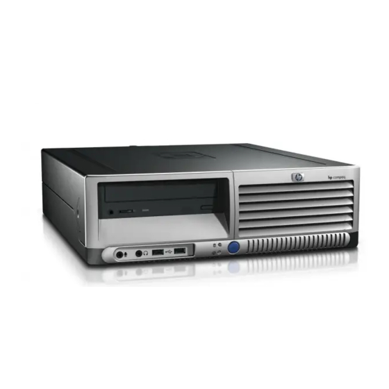
2.3.1 Cabinet Layouts Front Views Figure 2-2 shows the front panel components of the Ultra Slim Desktop (USDT) format factor. Item Description MultiBay device bay MultiBay device eject lever Microphone audio In jack Headphone audio Out jack Figure 2-2. HP Compaq dc7100 USDT Front View... - Page 22 Diskette drive media door CD-ROM drive acitvity LED Diskette drive eject button CD-ROM media tray CD-ROM drive open/close button Figure 2-3. HP Compaq dc7100 SFF Front View Item Decription Microphone audio In jack Headphone audio Out jack USB ports 7, 8...
- Page 23 Micorphone audio In jack Headphone audio Out jack USB ports 7, 8 hard drive activity LED Power LED Power button Figure 2-4. HP Compaq dx6100 ST Front View Technical Reference Guide Item Decription Diskette drive activity LED Diskette media door...
- Page 24 CD-ROM drive CD-ROM drive activity LED Diskette drive media door Diskette drive activity LED Diskette drive eject button USB ports 7, 8 Figure 2-5. HP Compaq dx6100 MT Front View Item Decription CD-ROM drive open/close button Power button Power LED...
- Page 25 CD-ROM drive CD-ROM drive activity LED Diskette drive media door Diskette drive activity LED Diskette drive eject button Hard drive activity LED Figure 2-6. HP Compaq dc7100 CMT Front View Technical Reference Guide Item Decription CD-ROM drive open/close button Power button...
- Page 26 NIC (LAN) connector (RJ-45) VGA monitor connector (DB-15) AC input connector USB ports 1, 2 USB ports 3 - 6 Figure 2-7. HP Compaq dc7100 USDT, Rear View 2-10 Item Description Mouse connector (PS/2) Keyboard connector (PS/2) Line audio In...
- Page 27 USB ports 3 - 6 Parallel port (DB-25) Serial port (DB-9) AC input connector USB ports 1, 2 Figure 2-8. HP Compaq dc7100 SFF, Rear Views Technical Reference Guide SFF chassis without card cage SFF Chassis with card cage Item Description...
- Page 28 Parallel port (DB-25) USB ports 3 - 6 NIC (LAN) connector (RJ-45) Serial port (DB-9) Headphone / Speaker audio Out Figure 2-9. HP Compaq dc7100 ST, Rear Views 2-12 ST chassis with card cage Item Description Line audio In Keyboard connector (PS/2)
- Page 29 VGA monitor connector (B-15) Microphone In jack USB ports 5, 6 NOTE: [1] Switch not present on SKUs that feature auto-ranging power supply. Figure 2-10. HP Compaq dx6100 MT, Rear View Technical Reference Guide Item Description Mouse connector (PS/2) Parallel port connctor (DB-25)
- Page 30 USB ports 5, 6 Microphone audio In VGA monitor connector (DB-15) Serial port connector (DB-9) Keyboard connector (PS/2)) AC line connector Figure 2-11. HP Compaq dc7100 CMT, Rear View 2-14 Item Description Mouse connector (PS/2) Parallel port connector (DB-25) USB ports 1-4...
-
Page 31: Chassis Layouts
UIltra Slim Desktop Chassis The Ultra Slim Desktop (USDT) chassis used for the HP Compaq dc7100 models uses a compact, space-saving form factor. Item Figure 2-12. - Page 32 Small Form Factor / Slim Tower Chassis The chassis layouts for the Small Form Factor (SFF) used for the HP Compaq dc7100 models and the Slim Tower (ST) used for the HP Comapq dx6100 models are shown in Figure 2-13. Features include: ■...
-
Page 33: Microtower Chassis
Microtower Chassis Figure 2-14 shows the layout for the Microtower (MT) chassis used for the HP Compaq dx6100 models. Features include: ■ Externally accessible drive bay assembly. ■ Easy access to expansion slots and all socketed system board components. Item... - Page 34 System Overview Convertible Minitower Figure 2-15 shows the layout for the Convertible Minitower (CMT) chassis in the minitower configuration used for HP Compaq dc7100 models. Features include: ■ Externally accessible drive bay assembly may be configured for minitower (vertical) or desktop (horizontal) position.
-
Page 35: Board Layouts
2.3.3 Board Layouts Figures 2-16 through 2-18 show the system and expansion boards for these systems. NOTE: See USDT rear chassis illustrations for externally accessible I/O connectors. Item Description Hood sense header Battery Parallel port option header Serial port A header Password clear jumper header SATA #0 header PCI 2.3 slot... - Page 36 System Overview Item Description Serial port B header Battery SATA #1 header SATA #0 header Password jumper PCI Express x1 slot PCI Express x16 graphics/reversed-layout SDVO slot PCI 2.3 slots Power supply (VccP) connector Processor socket Chassis fan, primary connector Chassis fan, secondary conenctor Power button, power LED, HD LED header NOTE:...
- Page 37 PCI Expansion Board [1] Item Description PCI 2.3 slots Battery PCI Express x1 slot PCI Express x16 graphics/normal-layout SDVO slot Chassis fan header Power supply (VccP) connector Serial port B header [2] Processor socket Processor fan connector DIMM sockets (4) MultiBay conector [2] Diskette drive connector Parallel ATA connector...
-
Page 38: System Architecture
System Overview 2.4 System Architecture The systems covered in this guide feature an architecture based on the Intel Pentium 4 processor and the Intel 915G chipset (Figure 2-11). These systems allow processor upgrading with the Intel Pentium 4 family and offer flexibility in expansion capabilities. All systems covered in this guide include the following key components: ■... - Page 39 Monitor PCI Express x16 slot (PEG)[1] SATA Hard Drive MultiBay Device CD-ROM AC97 Audio Subsystem Note: [1] SFF, ST, MT, and CMT form factors only. [2] 82915GV for USDT form factor 82915G for SFF. ST. MT, and CMT form factors Figure 2-19 System Architecture, Block diagram Technical Reference Guide Pentium 4...
-
Page 40: Intel Pentium 4 Processor
System Overview 2.4.1 Intel Pentium 4 Processor The models covered in this guide feature the Intel Pentium 4 processor with Hyper-Threading technology. This processor is backward-compatible with software written for the Pentium III, Pentium II, Pentium MMX, Pentium Pro, Pentium, and x86 microprocessors. The processor architecture includes a floating-point unit, 32-KB first and 1-MB secondary caches, and enhanced performance for multimedia applications through the use of multimedia extension (MMX) instructions. -
Page 41: Chipset
PCI 2.3 bus I/F PCI Express x1 LPC bus I/F SMBus I/F IDE I/F with SATA and PATA support AC ’97 controller RTC/CMOS IRQ controller Power management logic USB 1.1/2.0 controllers supporting eight (8) ports Loaded with HP/Compaq BIOS 361834-002 System Overview 2-25... -
Page 42: Support Components
System Overview 2.4.3 Support Components Input/output functions not provided by the chipset are handled by other support components. Some of these components also provide “housekeeping” and various other functions as well. Table 2-4 shows the functions provided by the support components. Support Component Functions Component Name LPC47B397 I/O Controller... -
Page 43: Mass Storage
2.4.5 Mass Storage All models support at least two mass storage devices, with one being externally accessible for removable media. These systems provide one, two, or four SATA interfaces and one PATA interface. These systems may be preconfigured or upgraded with a 40-, 80-, or 160-GB SATA hard drive and one removable media drive such as a CD-ROM drive. -
Page 44: Graphics Subsystem
System Overview 2.4.9 Graphics Subsystem These systems use the 82915G or 82915GV GMCH component that integrates an Intel graphics controller that can drive an external VGA monitor. The integrated graphics controller (IGC) features a 333-MHz core processor and a 400-MHz RAMDAC. The controller implements Dynamic Video Memory Technology (DVMT 3.0) for video memory. -
Page 45: Specifications
2.5 Specifications This section includes the environmental, electrical, and physical specifications for the systems covered in this guide. Where provided, metric statistics are given in parenthesis. Specifications are subject to change without notice. Environmental Specifications (Factory Configuration) Parameter Ambient Air Temperature Shock (w/o damage) Vibration Humidity... - Page 46 [1] System weight may vary depending on installed drives/peripherals. [2] Without MultiBay device installed. [3] Minitower configuration. For desktop configuration, swap Height and Width dimensions. [4] Applicable To unit in desktop orientation only and assumes reasonable type of load such as a monitor. 2-30...
- Page 47 Diskette Drive Specifications Parameter Media Type Height Bytes per Sector Sectors per Track: High Density Low Density Tracks per Side: High Density Low Density Read/Write Heads Average Access Time: Track-to-Track (high/low) Average (high/low) Settling Time Latency Average Technical Reference Guide Table 2-9 Measurement 3.5 in 1.44 MB/720 KB diskette...
-
Page 48: Optical Drive Specifications
System Overview Parameter Interface Type Media Type (reading) Media Type (writing) Transfer Rate (Reads) Transfer Rate (Writes): Capacity: Mode 1, 12 cm Mode 2, 12 cm 8 cm Center Hole Diameter Disc Diameter Disc Thickness Track Pitch Laser Beam Divergence Output Power Type Wave Length... - Page 49 Parameter Drive Size Interface Transfer Rate Drive Protection System Support? Typical Seek Time (w/settling) Single Track Average Full Stroke Disk Format (logical blocks) Rotation Speed Drive Fault Prediction Technical Reference Guide Table 2-11 Hard Drive Specifications 40 GB 80 GB 3.5 in 3.5 in SATA...
- Page 50 System Overview 2-34 361834-002 Technical Reference Guide...
-
Page 51: Processor/Memory Subsystem
Introduction This chapter describes the processor/memory subsystem. These systems feature the Intel Pentium 4 processor and the 915G chipset (Figure 3-1). The dx6100 and dc7100 models support PC2700 or PC3200 DDR memory and come standard with PC3200 DIMMs installed. The dx6120 models support PC2-4300 DDR2 DIMMs only. -
Page 52: Pentium 4 Processor
Processor/Memory Subsystem 3.2 Pentium 4 Processor These systems each feature an Intel Pentium 4 processor in a FC-LGA775 package mounted with a passive heat sink in a zero-insertion force socket. The mounting socket allows the processor to be easily changed for servicing and/or upgrading. 3.2.1 Processor Overview The Intel Pentium 4 processor represents the latest generation of Intel's IA32-class of processors. -
Page 53: Processor Upgrading
Figure 3-2 illustrates the internal architecture of the Intel Pentium 4 processor. Branch Prediction Rapid Exe. Eng. Core speed Pentium Type P4 560 P4 550 P4 540 P4 530 P4 520 Figure 3-2. Pentium 4 Processor Internal Architecture The Intel Pentium 4 increases processing speed by using higher clock speeds with hyper-pipelined technology, therefore handling significantly more instructions at a time. -
Page 54: Memory Subsystem
The SPD format supported by these systems complies with the JEDEC specification for 128-byte EEPROMs. This system also provides support for 256-byte EEPROMs to include additional HP-added features such as part number and serial number. The SPD format as supported in this system (SPD rev. 1) is shown in Table 3-1. - Page 55 Table 3-1 shows suggested memory configurations for these systems. NOTE: Table 3-1 does not list all possible configurations. Balanced-capacity, dual-channel loading yields best performance. Channel A Socket 1 Socket 2 [1] 128-MB 128-MB 128-MB 128-MB 256-MB 256-MB 512-MB 512-MB 1-GB 1-GB 1-GB 1-GB...
- Page 56 [8] Field specified as optional by JEDEC but required by this system. [9] HP usage. This system requires that the DIMM EEPROM have this space available for reads/writes. [10] Serial # in ASCII format (MSB is 133). Intended as backup identifier in case vender data is invalid.
- Page 57 Figure 3-3 shows the system memory map. Main Memory Area Compatibilty Area ✎ All locations in memory are cacheable. Base memory is always mapped to DRAM. The next 128 KB fixed memory area can, through the north bridge, be mapped to DRAM or to PCI space. Graphics RAM area is mapped to PCI or AGP locations.
- Page 58 Processor/Memory Subsystem 361834-002 Technical Reference Guide...
-
Page 59: Pci Bus Overview
Introduction This chapter covers subjects dealing with basic system architecture and covers the following topics: ■ PCI bus overview (4.2), page 4-1 ■ System resources (4.3), page 4-11 ■ Real-time clock and configuration memory (4.4), page 4-19 ■ System management (4.5), page 4-21 ■... -
Page 60: Pci Bus Transactions
System Support 82915G/GV [1] GMCH Memory Cntlr Function PCI Bus 0 Host-DMI Bridge DMI Link PCI 2.3 PCI Exp. Bridge Port 1 Function Function Notes: [1] USDT form factor; 82915GV; SFF, ST, MT, and CMT form factors, 82915G [2] SFF. ST, MT, and CMT form factors only. Figure 4-1. - Page 61 Configuration Cycles Devices on the PCI bus must comply with PCI protocol that allows configuration of that device by software. In this system, configuration mechanism #1 (as described in the PCI Local Bus specification Rev. 2.3) is employed. This method uses two 32-bit registers for initiating a configuration cycle for accessing the configuration space of a PCI device.
- Page 62 System Support Table 4-1 shows the standard configuration of device numbers and IDSEL connections for components and slots residing on a PCI 2.3 bus. PCI Component 82915G GMCH: Host/DMI Bridge Host/PCI Expr. Bridge Integrated Graphics Cntlr. PCI Express x16 graphics slot [1] 82801EB ICH6 PCI Bridge LPC Bridge...
-
Page 63: Pci Bus Master Arbitration
The register index (CF8h, bits <7..2>) identifies the 32-bit location within the configuration space of the PCI device to be accessed. All PCI devices can contain up to 256 bytes of configuration data (Figure 4-3), of which the first 64 bytes comprise the configuration space header. -
Page 64: Pci Express Bus Operation
System Support PCI Bus Mastering Devices Device PCI Connector Slot 1 PCI Connector Slot 2 PCI Connector Slot 3 PCI Connector Slot 4 NOTE: [1]SFF, ST, MT, and CMT form factors only. [2] CMT form factor with PCI expansion board PCI bus arbitration is based on a round-robin scheme that complies with the fairness algorithm specified by the PCI specification. - Page 65 Link Layer The link layer provides data integrity by adding a sequence information prefix and a CRC suffix to the packet created by the transaction layer. Flow-control methods ensure that a packet will only be transferred if the receiving device is ready to accomodate it. A corrupted packet will be automatically re-sent.
-
Page 66: Option Rom Mapping
System Support For a PCI Express x16 transfer, a lane will be re-used every17th byte of a transfer. The mux-demux process provided by the physical layer is transparent to the other layers and to software/drivers. The SFF, ST, MT MT, and CMT forma factors provide two PCI Express slots: a PCI Express x16 (16-lane) slot specifically designed for a graphics controller, and a general purpose PCI Express x1 (1-lane) slot. -
Page 67: Pci Connector
4.2.6 PCI Connectors PCI 2.3 Connector Figure 4-5. PCI 2.3 Bus Connector (32-Bit, 5.0-volt Type) B Signal A Signal -12 VDC TRST- +12 VDC +5 VDC +5 VDC +5 VDC INTA- INTB- INTC- INTD- +5 VDC PRSNT1- Reserved RSVD +5 VDC PRSNT2- Reserved RSVD... -
Page 68: Pci Express Connectors
System Support PCI Express Connectors x1 Connector x16 Connector Figure 4-6. PCI Express Bus Connectors B Signal A Signal +12 VDC PRSNT1# +12 VDC +12 VDC RSVD +12 VDC SMCLK +5 VDC +5 VDC JTAG2 JTAG4 +3.3 VDC JTAG5 JTAG1 +3.3 VDC 3.3 Vaux +3.3 VDC... -
Page 69: System Resources
4.3 System Resources This section describes the availability and basic control of major subsystems, otherwise known as resource allocation or simply “system resources.” System resources are provided on a priority basis through hardware interrupts and DMA requests and grants. 4.3.1 Interrupts The microprocessor uses two types of hardware interrupts;... - Page 70 System Support 8259 Mode The 8259 mode handles interrupts IRQ0-IRQ15 in the legacy (AT-system) method using 8259-equivalent logic. Table 4-7 lists the standard source configuration for maskable interrupts and their priorities in 8259 mode. If more than one interrupt is pending, the highest priority (lowest number) is processed first.
-
Page 71: Apic Mode
APIC Mode The Advanced Programmable Interrupt Controller (APIC) mode provides enhanced interrupt processing with the following advantages: ■ Eliminates the processor's interrupt acknowledge cycle by using a separate (APIC) bus ■ Programmable interrupt priority ■ Additional interrupts (total of 24) The APIC mode accommodates eight PCI interrupt signals (INTA-..INTH-) for use by PCI devices. -
Page 72: Non-Maskable Interrupts
System Support Maskable Interrupt processing is controlled and monitored through standard AT-type I/O-mapped registers. These registers are listed in Table 4-8. Maskable Interrupt Control Registers I/O Port Register 020h Base Address, Int. Cntlr. 1 021h Initialization Command Word 2-4, Int. Cntlr. 1 0A0h Base Address, Int. - Page 73 The NMI Status Register at I/O port 061h contains NMI source and status data as follows: NMI Status Register 61h Function NMI Status: 0 = No NMI from system board parity error. 1 = NMI requested, read only IOCHK- NMI: 0 = No NMI from IOCHK- 1 = IOCHK- is active (low), NMI requested, read only Interval Timer 1, Counter 2 (Speaker) Status...
-
Page 74: Direct Memory Access
System Support 4.3.2 Direct Memory Access Direct Memory Access (DMA) is a method by which a device accesses system memory without involving the microprocessor. Although the DMA method has been traditionally used to transfer blocks of data to or from an ISA I/O device, PCI devices may also use DMA operation as well. The DMA method reduces the amount of CPU interactions with memory, freeing the CPU for other processing tasks. - Page 75 DMA Page Registers The DMA page register contains the eight most significant bits of the 24-bit address and works in conjunction with the DMA controllers to define the complete (24-bit) address for the DMA channels. Table 4-10 lists the page register port addresses. DMA Page Register Addresses DMA Channel Controller 1 (byte transfers)
- Page 76 System Support The remaining address lines are in an undefined state during the refresh cycle. The refresh operations are driven by a 69.799-KHz clock generated by Interval Timer 1, Counter 1. The refresh rate is 128 refresh cycles in 2.038 ms. DMA Controller Registers Table 4-11 lists the DMA Controller Registers and their I/O port addresses.
-
Page 77: Real-Time Clock And Configuration Memory
4.4 Real-Time Clock and Configuration Memory The Real-time clock (RTC) and configuration memory (also referred to as “CMOS”) functions are provided by the 82801 component and is MC146818-compatible. As shown in the following figure, the 82801 ICH6 component provides 256 bytes of battery-backed RAM divided into two 128-byte configuration memory areas. -
Page 78: Cmos Archive And Restore
System Support 4.4.2 CMOS Archive and Restore During the boot sequence the BIOS saves a copy of NVRAM (CMOS contents, password(s) and other system variables) in a portion of the flash ROM. Should the system become un-usable, the last good copy of NVRAM data can be restored with the Power Button Override function. This function is invoked with the following procedure: 1. -
Page 79: Standard Cmos Locations
4.4.3 Standard CMOS Locations Table 4-12 describes standard configuration memory locations 0Ah-3Fh. These locations are accessible through using OUT/IN assembly language instructions using port 70/71h or BIOS function INT15, AX=E823h. Location Function 00-0Dh Real-time clock Diagnostic status System reset code Diskette drive type Reserved Hard drive type... -
Page 80: Setup Password
System Support Power-On / Setup Password These systems include a power-on and setup passwords, which may be enabled or disabled (cleared) through a jumper on the system board. The jumper controls a GPIO input to the 82801 ICH6 that is checked during POST. The password is stored in configuration memory (CMOS) and if enabled and then forgotten by the user will require that either the password be cleared (preferable solution and described below) or the entire CMOS be cleared (refer to section 4.4.1). -
Page 81: Power Management
Level 0—Cover removal indication is essentially disabled at this level. During POST, status bit is cleared and no other action is taken by BIOS. Level 1—During POST the message “The computer's cover has been removed since the last system start up” is displayed and time stamp in CMOS is updated. Level 2—During POST the “The computer's cover has been removed since the last system start up”... -
Page 82: System Status
System Support 4.5.3 System Status These systems provide a visual indication of system boot and ROM flash status through the keyboard LEDs and operational status using bi-colored power and hard drive activity LEDs as indicated in Tables 4-13 and 4-14 respectively. ✎... -
Page 83: Thermal Sensing And Cooling
4.5.4 Thermal Sensing and Cooling All systems feature a variable-speed fan mounted as part of the processor heatsink assembly. All systems also provide or support an auxiliary chassis fan. All fans are controlled through temperature sensing logic on the system board and/or in the power supply. There are some electrical differences between form factors and between some models, although the overall functionally is the same. -
Page 84: Register Map And Miscellaneous Functions
System Support 4.6 Register Map and Miscellaneous Functions This section contains the system I/O map and information on general-purpose functions of the ICH6 and I/O controller. 4.6.1 System I/O Map Table 4-15 lists the fixed addresses of the input/output (I/O) ports. I/O Port Function 0000..001Fh... -
Page 85: Lpc47B397 I/O Controller Functions
4.6.2 LPC47B397 I/O Controller Functions The LPC47B397 I/O controller contains various functions such as the keyboard/mouse interfaces, diskette interface, serial interfaces, and parallel interface. While the control of these interfaces uses standard AT-type I/O addressing (as described in chapter 5) the configuration of these functions uses indexed ports unique to the LPC47B397. - Page 86 System Support The configuration registers are accessed through I/O registers 2Eh (index) and 2Fh (data) after the configuration phase has been activated by writing 55h to I/O port 2Eh. The desired interface (logical device) is initiated by firmware selecting logical device number of the 47B347 using the following sequence: 1.
-
Page 87: Input/Output Interfaces
Introduction This chapter describes the standard (i.e., system board) interfaces that provide input and output (I/O) porting of data and specifically discusses interfaces that are controlled through I/O-mapped registers. The following I/O interfaces are covered in this chapter: ■ PATA/SATA interface (5.2), page 5-1 ■... - Page 88 Input/Output Interfaces IDE Configuration Registers The IDE controller is configured as a PCI device with bus mastering capability. The PCI configuration registers for the IDE controller function (PCI device #31, function #1) are listed in Table 5-1. PCI Conf. Address Register 00-01h Vender ID...
- Page 89 IDE Bus Master Control Registers The IDE interface can perform PCI bus master operations using the registers listed in Table 5-2. These registers occupy 16 bytes of variable I/O space set by software and indicated by PCI configuration register 20h in the previous table. IDE Bus Master Control Registers Address Size...
- Page 90 Input/Output Interfaces Signal Description RESET- Reset Ground Data Bit <7> Data Bit <8> Data Bit <6> Data Bit <9> Data Bit <5> DD10 Data Bit <10> Data Bit <4> DD11 Data Bit <11> Data Bit <3> DD12 Data Bit <12> Data Bit <2>...
-
Page 91: Enhanced Ide/Sata Interfaces
SATA Interfaces These systems provide one, two, or four serial ATA (SATA) interfaces that can provide certain advantages over legacy EIDE (PATA) interface including: ■ Higher transfer rates: up to 1.5 Gb/s (150 MB/s) ■ Reduced wiring (smaller cable assemblies) The SATA interface duplicates most of the functionality of the EIDE interface through a register interface that is equivalent to that of the legacy IDE host adapter. -
Page 92: Sata Connector
Input/Output Interfaces SATA Bus Master Control Registers The SATA interface can perform PCI bus master operations using the registers listed in Table 5-5. These registers occupy 16 bytes of variable I/O space set by software and indicated by PCI configuration register 20h in the previous table. As indicated, these registers are virtually a copy of those used by EIDE operations discussed in the EIDE section. -
Page 93: Diskette Drive Interface
5.3 Diskette Drive Interface The diskette drive interface in these systems support one diskette drive connected to a standard 34-pin diskette drive connector. Selected models come standard with a 3.5-inch 1.44-MB diskette drive installed as drive A. The diskette drive interface function is integrated into the LPC47B397 super I/O component. The internal logic of the I/O controller is software-compatible with standard 82077-type logic. - Page 94 Input/Output Interfaces Diskette Drive Interface Configuration Registers Index Address 60-61h DMA Channel Select For detailed configuration register information refer to the SMSC data sheet for the LPC47B397 I/O component. Table 5-7. Function Activate Base Address Interrupt Select DD Mode DD Option DD Type DD 0 DD 1...
- Page 95 Diskette Drive Interface Control The BIOS function INT 13 provides basic control of the diskette drive interface. The diskette drive interface can be controlled by software through the LPC47B397's I/O-mapped registers listed in Table 5-8. The diskette drive controller of the LPC47B397 operates in the PC/AT mode in these systems.
- Page 96 Input/Output Interfaces Primary Second. Address Address Register 3F4h 374h 3F5h 375h 3F6h 376h 3F7h 377h NOTE: The most recently written data rate value to either DRSR or CCR will be in effect. 5-10 Table 5-8. (Continued) Diskette Drive Interface Control Registers Main Status Register (MSR): <7>...
-
Page 97: Diskette Drive Connector
5.3.2 Diskette Drive Connector This system uses a standard 34-pin connector (refer to Figure 5-3 and Table 5-9 for the pinout) for diskette drives. Drive power is supplied through a separate connector. Figure 5-3. 34-Pin Diskette Drive Connector. Signal Description Ground LOW DEN- Low density select... -
Page 98: Serial Interface
Input/Output Interfaces 5.4 Serial Interface Systems covered in this guide may include one RS-232-C type serial interface to transmit and receive asynchronous serial data with external devices. Some systems may allow the installation of a second serial interface through an adapter that consists of a PCI bracket and a cable that attaches to header P52 on the system board. - Page 99 The serial interface configuration registers are listed in the following table: Serial Interface Configuration Registers Index Address Serial Interface Control The BIOS function INT 14 provides basic control of the serial interface. The serial interface can be directly controlled by software through the I/O-mapped registers listed in Table 5-12. COM1 COM2 Addr.
-
Page 100: Parallel Interface
Input/Output Interfaces 5.5 Parallel Interface Systems covered in this guide may include a parallel interface for connection to a peripheral device with a compatible interface, the most common being a printer. The parallel interface function is integrated into the LPC47B397 I/O controller component and provides bi-directional 8-bit parallel data transfers with a peripheral device. -
Page 101: Extended Capabilities Port Mode
5.5.3 Extended Capabilities Port Mode The Extended Capabilities Port (ECP) mode, like EPP, also uses a hardware protocol-based design that supports transfers up to 2 MB/s. Automatic generation of addresses and strobes as well as Run Length Encoding (RLE) decompression is supported by ECP mode. The ECP mode includes a bi-directional FIFO buffer that can be accessed by the CPU using DMA or programmed I/O. - Page 102 Input/Output Interfaces Parallel Interface Control The BIOS function INT 17 provides simplified control of the parallel interface. Basic functions such as initialization, character printing, and printer status are provide by subfunctions of INT 17. The parallel interface is controllable by software through a set of I/O mapped registers. The number and type of registers available depends on the mode used (SPP, EPP, or ECP).
-
Page 103: Parallel Interface Connector
5.5.5 Parallel Interface Connector Figure 5-5 and Table 5-15 show the connector and pinout of the parallel interface connector. Note that some signals are redefined depending on the port's operational mode. Figure 5-5. Parallel Interface Connector (Female DB-25 as viewed from rear of chassis) Signal Function STB-... -
Page 104: Keyboard/Pointing Device Interface
Input/Output Interfaces 5.6 Keyboard/Pointing Device Interface The keyboard/pointing device interface function is provided by the LPC47B397 I/O controller component, which integrates 8042-compatible keyboard controller logic (hereafter referred to as simply the “8042”) to communicate with the keyboard and pointing device using bi-directional serial data transfers. - Page 105 Table 5-16 lists and describes commands that can be issued by the 8042 to the keyboard. Command Set/Reset Status Indicators Echo Invalid Command Select Alternate Scan Codes Read ID Set Typematic Rate/Display Enable Default Disable Set Default Set Keys—Typematic Technical Reference Guide Table 5-16.
-
Page 106: Pointing Device Interface Operating
Input/Output Interfaces Command Set Keys—Make/Brake Set Keys—Make Set Keys— Typematic/Make/Brake Set Type Key—Typematic Set Type Key—Make/Brake Set Type Key—Make Resend Reset Note: [1] Used in Mode 3 only. 5.6.2 Pointing Device Interface Operating The pointing device (typically a mouse) connects to a 6-pin DIN-type connector that is identical to the keyboard connector both physically and electrically. - Page 107 The keyboard interface configuration registers are listed in the following table: Keyboard Interface Configuration Registers Index Address Function Activate Primary Interrupt Select Secondary Interrupt Select Reset and A20 Select 8042 Control The BIOS function INT 16 is typically used for controlling interaction with the keyboard. Sub-functions of INT 16 conduct the basic routines of handling keyboard data (i.e., translating the keyboard's scan codes into ASCII codes).
- Page 108 Input/Output Interfaces I/O Port 64h I/O port 64h is used for reading the status register and for writing commands. A read of 64h by the CPU will yield the status byte defined as follows: Function 7..4 General Purpose Flags. CMD/DATA Flag (reflects the state of A2 during a CPU write). 0 = Data 1 = Command General Purpose Flag.
- Page 109 Value Command Description Test the clock and data lines of the pointing device interface and place test results in the output buffer. 00h = No error detected 01h = Clock line stuck low 02h = Clock line stuck high 03h = Data line stuck low 04h = Data line stuck high Initialization.
-
Page 110: Keyboard/Pointing Device Interface Connector
Input/Output Interfaces 5.6.4 Keyboard/Pointing Device Interface Connector The legacy-light model provides separate PS/2 connectors for the keyboard and pointing device. Both connectors are identical both physically and electrically. Figure 5-7 and Table 5-19 show the connector and pinout of the keyboard/pointing device interface connectors. Figure 5-7. -
Page 111: Universal Serial Bus Interface
5.7 Universal Serial Bus Interface The Universal Serial Bus (USB) interface provides asynchronous/isochronous data transfers with compatible peripherals such as keyboards, printers, or modems. This high-speed interface supports hot-plugging of compatible devices, making possible system configuration changes without powering down or even rebooting systems. As shown in Figure 5-8, the USB interface is provided by the 82801 component. -
Page 112: Usb Data Formats
Input/Output Interfaces 5.7.1 USB Data Formats The USB I/F uses non-return-to-zero inverted (NRZI) encoding for data transmissions, in which a 1 is represented by no change (between bit times) in signal level and a 0 is represented by a change in signal level. Bit stuffing is employed prior to NRZ1 encoding so that in the event a string of 1's is transmitted (normally resulting in a steady signal level) a 0 is inserted after every six consecutive 1's to ensure adequate signal transitions in the data stream. -
Page 113: Usb Programming
5.7.2 USB Programming Programming the USB interface consists of configuration, which typically occurs during POST, and control, which occurs at runtime. USB Configuration Each USB controller functions as a PCI device within the 82801 component and is configured using PCI Configuration Registers as listed in Table 5-20. NOTE: PCI Config. -
Page 114: Usb Connector
Input/Output Interfaces USB Control The USB is controlled through I/O registers as listed in table 5-21. I/O Address Register 00, 01h Command 02, 03h Status 04, 05h Interupt Enable 06, 07 Frame Number 08, 0B Frame List Base Address Start of Frame Modify 10, 11h Port 1 Status/Control 12, 13h... -
Page 115: Usb Cable Data
5.7.4 USB Cable Data The recommended cable length between the host and the USB device should be no longer than sixteen feet for full-channel (12 MB/s) operation, depending on cable specification (see following table). Conductor Size 20 AWG 22 AWG 24 AWG 26 AWG 28 AWG... -
Page 116: Audio Subsystem
CD Audio (R) Audio Bias Mic In Figure 5-11. Audio Subsystem Functional Block Diagram 5-30 PC Beep Audio AC97 Link Bus Mono Audio 7056 Spkr Mute Audio Codec HP Out Audio (L/R) 361834-002 Internal Speaker Headphones/ Line Out Technical Reference Guide... -
Page 117: Ac97 Audio Controller
5.8.1 AC97 Audio Controller The AC97 Audio Controller is a PCI device that is integrated into the 82801 ICH component and supports the following functions: ■ Read/write access to audio codec registers ■ 16-bit stereo PCM output @ up to 48 KHz sampling ■... -
Page 118: Audio Codec
Mic In Line In (L) Line In (R) CD In (L) CD In (R) SPDIF HP Out L Analog Output HP Out R Circuits Figure 5-13. AD1981B Audio Codec Functional Block Diagram All inputs and outputs are two-channel stereo except for the microphone input, which is inputted as a single-channel but mixed internally onto both left and right channels. -
Page 119: Audio Programming
5.8.4 Audio Programming Audio subsystem programming consists configuration, typically accomplished during POST, and control, which occurs during runtime. Audio Configuration The audio subsystem is configured according to PCI protocol through the AC97 audio controller function of the 82801 ICH. Table 5-24 lists the PCI configuration registers of the audio subsystem. - Page 120 Input/Output Interfaces Audio Control The audio subsystem is controlled through a set of indexed registers that physically reside in the audio codec . The register addresses are decoded by the audio controller and forwarded to the audio codec over the AC97 Link Bus previously described. The audio codec's control registers (Table 5-25) are mapped into 64 kilobytes of variable I/O space.
-
Page 121: Audio Specifications
Mic Input A/D (PC record) Line input Mic input D/A (PC playback) Max. Power Output (with 10% THD): Small Form Factor Slim Desktop/Configurable Minitower Input Gain Attenuation Range Master Volume Range Frequency Response: Codec Speaker (Small Form Factor) Technical Reference Guide Table 5-26. -
Page 122: Network Interface Controller
Input/Output Interfaces 5.9 Network Interface Controller These systems provide 10/100/1000 Mbps network support through a Broadcom BCM5751 network interface controller (NIC), a PHY component, and a RJ-45 jack with integral status LEDs. The 82562-equivalent controller integrated into the 82801 ICH component is not used (disabled) in these systems. -
Page 123: Wake-On-Lan Support
5.9.1 Wake-On-LAN Support The NIC supports the Wired-for-Management (WfM) standard of Wake-On-LAN (WOL) that allows the system to be booted up from a powered-down or low-power condition upon the detection of special packets received over a network. The NIC receives 3.3 VDC auxiliary power while the system unit is powered down in order to process special packets. -
Page 124: Nic Programming
The Broadcom BCM5782 is configured as a PCI device and controlled through registers mapped in variable I/O space. The BIOS for the BCM5782 is contained within the HP/Compaq BIOS in system ROM. Refer to Broadcom documentation for details regarding BCM5782 register programming. -
Page 125: Nic Specifications
5.9.6 NIC Specifications Parameter Modes Supported Standards Compliance OS Driver Support Boot ROM Support F12 BIOS Support Bus Inteface Power Management Support Technical Reference Guide Table 5-27. NIC Specifications 10BASE-T half duplex @ 10 Mb/s 10Base-T full duplex @ 20 Mb/s 100BASE-TX half duplex @ 100 Mb/s 100Base-TX full duplex @ 200 Mb/s 1000BASE-T half duplex @ 1 Gb/s... - Page 126 Input/Output Interfaces 5-40 361834-002 Technical Reference Guide...
-
Page 127: Integrated Graphics Subsystem
Integrated Graphics Subsystem Introduction This chapter describes graphics subsystem that is integrated into the 82915G/GV GMCH component. This graphics subsystem employs the use of system memory to provide efficient, economical 2D and 3D performance. The SFF, ST, MT, and CMT form factors may be upgraded by installing a graphics card into the PCI Express x16 or the PCI 2.3 slot. -
Page 128: Functional Description
Integrated Graphics Subsystem 6.2 Functional Description The Intel 915G/GV GMCH component includes an integrated graphics controller (IGC). (Figure 6-1). The IGC can directly drive an external, analog multi-scan monitor at resolutions up to and including 2048 x 1536 pixels. The IGC includes a memory management feature that allocates portions of system memory for use as the frame buffer and for storing textures and 3D effects. - Page 129 The graphics controller integrated into the 82915G/GV GMCH component includes 2D and 3D accelerator engines working with a deeply-pipelined pre-processor. Hardware cursor and overlay generators are also included as well as a legacy VGA processor core. The IGC supports three display devices: ■...
-
Page 130: Video Memory Allocation Reporting
Integrated Graphics Subsystem 6.2.1 Video Memory Allocation Reporting The IGC does not have local memory at its disposal but instead uses a portion of system memory allocated for frame buffering and texturing. The total memory allocation is determined by the amount of system memory installed in a system. -
Page 131: Display Modes
Depending on accessory, upgrading through the PCI Express x16 slot can provide digital monitor support and/or dual-monitor support allowing display-cloning or extended desktop functionality. Software drivers may need to be downloaded for specific cards. ✎ Two SDVO channels are provided by the IGC for supporting two digital displays. Existing option cards and drivers support one CRT and digital display. -
Page 132: Vga Monitor Connector
Integrated Graphics Subsystem 6.5 VGA Monitor Connector These systems includes a standard VGA connector (Figure 6-3) for attaching an analog monitor: Figure 6 3. VGA Monitor Connector, (Female DB-15, as viewed from rear). Signal Description Red Analog Blue Analog Green Analog Not Connected Ground R GND... -
Page 133: Power And Signal Distribution
Introduction This chapter describes the power supply and method of general power and signal distribution. Topics covered in this chapter include: ■ Power supply assembly/control (7.2), page 7-1 ■ Power distribution (7.3), page 7-8 ■ Signal distribution (7.4), page 7-13 Power Supply Assembly/Control These systems feature a power supply assembly that is controlled through programmable logic (Figure 7-1). -
Page 134: Power Supply Assembly
Power and Signal Distribution 7.2.1 Power Supply Assembly These systems feature power supplies with power factor-correction logic. Four power supplies are used: a 200-watt power supply for the USDT unit, a 240-watt power supply for the SFF and ST units, a 300-watt power supply for the MT unit, and a 340-watt power supply for the CMT unit. - Page 135 300-Watt (MT) Power Supply Assembly Specifications Input Line Voltage: 115 VAC Setting 230 VAC Setting Line Frequency Constant Input (AC) Current +3.3 VDC Output +5 VDC Output +5 AUX Output +12 VDC Output +12 VDC Output (Vcpu) --12 VDC Output NOTES: Total continuous power should not exceed 300 watts.
-
Page 136: Power Control
Power and Signal Distribution 7.2.2 Power Control The power supply assembly is controlled digitally by the PS On signal (Figure 7-1). When PS On is asserted, the Power Supply Assembly is activated and all voltage outputs are produced. When PS On is de-asserted, the Power Supply Assembly is off and no voltages (except +5 AUX) are generated. -
Page 137: Power Management
Power LED Indications A dual-color LED located on the front panel (bezel) is used to indicate system power status. The front panel (bezel) power LED provides a visual indication of key system conditions listed as follows: Power LED Steady green Blinks green @ 0.5 Hz Blinks red 2 times @ 1 Hz [1] Blinks red 3 times @ 1 Hz [1]... - Page 138 Power and Signal Distribution The wake up sequence for each event occurs as follows: Wake-On-LAN The network interface controller (NIC) can be configured for detection of a “Magic Packet” and wake the system up from sleep mode through the assertion of the PME- signal on the PCI bus. Refer to Chapter 5, “Network Support”...
-
Page 139: Power Management
7.2.3 Power Management These systems include power management functions designed to conserve energy. These functions are provided by a combination of hardware, firmware (BIOS) and software. The system provides the following power management features: ■ ACPI v1.0b compliant (ACPI modes C1, C2, S1, and S3, ) ■... -
Page 140: Power Distribution
The power supply assembly includes a multi-connector cable assembly that routes +3.3 VDC, +5 VDC, +5 VDC STB, +12 VC, and -12 VDC to the system board as well as to the individual drive assemblies. Figure 7-2 shows the power supply cabling for the Ultra Slim Desktop form factor. Power Supply... - Page 141 Figure 7-3 shows the power supply cabling for the SFF/ST systems. Power Supply 349318 Conn Pin 1 Pin 2 P1 [1] +5 sns P4, 5 +3.3 Connectors not shown to scale. All + and - values are VDC. RTN = Return (signal ground) sns = sense GND = Power ground RS = Remote sense...
- Page 142 Power and Signal Distribution Figure 7-4 shows the power supply cabling for the microtower systems. Power Supply 366307 Conn Pin 1 Pin 2 +3.3RS +3.3 P1 [1] +3.3 P2-6 P9, 10 +3.3 NOTES: Connectors not shown to scale. All + and - values are VDC. RTN = Return (signal ground) GND = Power ground RS = Remote sense...
- Page 143 Figure 7-4 shows the power supply cabling for the convertible minitower systems. Power Supply 349774 Conn Pin 1 Pin 2 +3.3 +3.3 P1 [1] P4, 5, +3.3 9, 10 P6, 7, NOTES: Connectors not shown to scale. All + and - values are VDC. RTN = Return (signal ground) GND = Power ground RS = Remote sense...
-
Page 144: Low Voltage Production/Distribution
Power and Signal Distribution 7.3.2 Low Voltage Production/Distribution Auxiliary voltages less than 5 volts and all voltages less than 3.3 volts are produced through regulator circuitry (Figure 7-6) on the system board. Power Supply Power Supply Power Supply Power Supply Processor Figure 7-6. -
Page 145: Signal Distribution
Hard Drive IDE I/F., Diskette I/F., MultiBay CD Audio Daughter Board Keyboard Kybd data Mouse Mouse data Mic In, HP Out Audio Front Panel USB 6,7 Tx/Rx I/O Module 361834-002 Power and Signal Distribution HD LED CD, DVD, or Diskette Drive... - Page 146 Supply PS On, POK Assembly Diskette Diskette I/F IDE I/F SATA Hard Drive CD-ROM IDE I/F Keyboard Kybd data Mouse Mouse data Mic In, HP Out Audio Front Panel USB 6,7 Tx/Rx I/O Module 361834-002 HD LED Technical Reference Guide...
- Page 147 Diskette Diskette I/F IDE I/F Hard Drive CD-ROM IDE I/F. Keyboard Kybd data Mouse data Mic In, HP Out Audio USB 6,7 Tx/Rx I/O Module PCI 2.3 I/F PCI Expansion Daughter Board [1] 361834-002 Power and Signal Distribution Power On...
- Page 148 Power and Signal Distribution Power Button/LED, HD LED Header P5 (USDT, SFF, ST) HD LED Cathode 1 HD LED Anode 3 GND5 Chassis ID0 9 GND 11 Therm Diode A 13 Serial Port A Header P54 UART1 DCD- 1 UART1 RX DATA 3 UART1 TX DATA 5 UART1 DTR 7 GND 9...
-
Page 149: Introduction
Introduction The Basic Input/Output System (BIOS) of the computer is a collection of machine language programs stored as firmware in read-only memory (ROM). The BIOS ROM includes such functions as Power-On Self Test (POST), PCI device initialization, Plug 'n Play support, power management activities, and the Setup utility. -
Page 150: Rom Flashing
All BIOS ROM upgrades are available directly from HP. Flashing is done either locally with the HP-provided Windows program, a ROMPaq diskette or remotely using the network boot function (described in the section 8.3.2). -
Page 151: Changeable Splash Screen
A corrupted splash screen may be restored by the user with the ROMPAQ software. Depending on the system, changing (customizing) the splash screen may only be available with asistance from HP. The splash screen (image displayed during POST) is stored in the BIOS ROM and may be replaced with another image of choice by using the Image Flash utility (Flashi.exe). -
Page 152: Network Boot (F12) Support
BIOS ROM 8.3.2 Network Boot (F12) Support The BIOS supports booting the system to a network server. The function is accessed by pressing the F12 key when prompted at the lower right hand corner of the display during POST. Booting to a network server allows for such functions as: ■... -
Page 153: Boot Error Codes
8.3.4 Boot Error Codes The BIOS provides visual and audible indications of a failed system boot by using the LEDS on the PS/2 keyboard and the system board speaker. The error conditions are listed in the following table. Visual [1] Num Lock LED blinks Scroll Lock LED blinks Caps Lock LED blinks... -
Page 154: Setup Utility
BIOS ROM 8.4 Setup Utility The Setup utility (stored in ROM) allows the user to configure system functions involving security, power management, and system resources. The Setup utility is ROM-based and invoked when the key is pressed and held during the computer boot cycle. Highlights of the Setup utility are described in the following table. - Page 155 Heading Option File Save Changes and (continued) Exit Storage Device Configuration ✎ Support for specific Computer Setup options may vary depending on the hardware configuration. Technical Reference Guide Table 8-3 Setup Utility Description Saves changes to system configuration or default settings and exits Computer Setup.
- Page 156 BIOS ROM Heading Option Storage Options ✎ Support for specific Computer Setup options may vary depending on the hardware configuration. Table 8-3 Setup Utility Description Translation Parameters (ATA disks only) ✎ This feature appears only when User translation mode is selected. Allows you to specify the parameters (logical cylinders, heads, and sectors per track) used by the BIOS to translate disk I/O requests (from the operating system or an application) into terms the hard...
- Page 157 Allows you to set and enable power-on password. See the Troubleshooting Guide for more information. Allows you to specify whether the password is required for warm boot (CTRL+ALT+DEL). See the Desktop Management Guide for more information. 361834-002 BIOS ROM...
- Page 158 Setup Password requires that the setup password be entered to boot the computer if the sensor detects that the cover has been removed. This feature is supported on select models only. See the Desktop Management Guide on the Documentation CD for more information.
- Page 159 ✎ This selection will only appear when at least one MultiBay drive that supports the DriveLock feature is attached to the system. See the Desktop Management Guide on the Documentation CD for more information. Enable/Disable. Data Execution Prevention Mode help prevent OS security breaches.
- Page 160 BIOS ROM Heading Option Restore Master Boot Record* Power OS Power Management Hardware Power Management Thermal ✎ Support for specific Computer Setup options may vary depending on the hardware configuration. 8-12 Table 8-3 Setup Utility Description Restores the backup Master Boot Record to the current bootable disk.
- Page 161 Heading Option Advanced* Power-On Options *For advanced users only ✎ Support for specific Computer Setup options may vary depending on the hardware configuration. Technical Reference Guide Table 8-3 Setup Utility Description Allows you to set: • POST mode (QuickBoot, FullBoot, or FullBoot every 1-30 days). •...
- Page 162 BIOS ROM Heading Option Advanced* Power-On Options (continued) (continued) *For advanced users only BIOS Power-On Onboard Devices PCI Devices Bus Options* ✎ Support for specific Computer Setup options may vary depending on the hardware configuration. 8-14 Table 8-3 Setup Utility Description Allows you to set: (continued) •...
- Page 163 Heading Option Advanced* Device options (continued) *For advanced users only PCI VGA Configuration ✎ Support for specific Computer Setup options may vary depending on the hardware configuration. Technical Reference Guide Table 8-3 Setup Utility Description Allows you to set: • Printer mode (bi-directional, EPP & ECP, output only). •...
-
Page 164: Client Management Functions
BIOS ROM 8.5 Client Management Functions Table 8-4 provides a partial list of the client management BIOS functions supported by the systems covered in this guide. These functions, designed to support intelligent manageability applications, are Compaq-specific unless otherwise indicated. Client Management Functions (INT15) Function E800h Get system ID... -
Page 165: System Id And Rom Type
8.5.1 System ID and ROM Type Diagnostic applications can use the INT 15, AX=E800h BIOS function to identify the type of system. This function will return the system ID in the BX register. systems have the following IDs and ROM family types: Table 8-5 System ID System (Form Factor) -
Page 166: Pnp Support
BIOS ROM 8.6 PnP Support The BIOS includes Plug 'n Play (PnP) support for PnP version 1.0A. Table 8-6 lists the PnP functions supported. PnP BIOS Functions Function Get number of system device nodes Get system device node Set system device node Get event Send message Get SMBIOS Structure Information... -
Page 167: Smbios
8.6.1 SMBIOS In support of the DMI specification the PnP functions 50h and 51h are used to retrieve the SMBIOS data. Function 50h retrieves the number of structures, size of the largest structure, and SMBIOS version. Function 51h retrieves a specific structure. This system supports SMBIOS version 2.3.1 and the following structure types: Type Data... - Page 168 BIOS ROM 8-20 361834-002 Technical Reference Guide...
-
Page 169: Error Messages And Codes
This appendix lists the error codes and a brief description of the probable cause of the error. ✎ Errors listed in this appendix are applicable only for systems running HP/Compaq BIOS. Not all errors listed in this appendix may be applicable to a particular system model and/or configuration. - Page 170 Error Messages and Codes A.3 Power-On Self Test (POST) Messages Error Message Invalid Electronic Serial Number Network Server Mode Active (w/o kybd) 101-Option ROM Checksum Error 110-Out of Memory Space for Option ROMs 102-system Board Failure 150-Safe POST Active 162-System Options Not Set 163-Time &...
- Page 171 Error Message 512-Chassis Fan Not Detected 514-CPU or Chassis Fan not detected. 601-Diskette Controller Error 605-Diskette Drive Type Error 912-Computer Cover Removed Since Last System Start Up 914-Hood Lock Coil is not Connected 916-Power Button Not Connected 917-Expansion Riser Not Detected 919-Front Panel, MultiPort, and/or MultiBay Risers not Detected 1156-Serial Port A Cable Not...
- Page 172 Error Messages and Codes Error Message 1794-Inaccessible devices attached to SATA 1 and/or SATA 3 (for systems with 4 SATA ports) 1796-SATA Cabling Error 1801-Microcode Patch Error 1998-Master Boot Record Backup Has Been Lost 1999-Master Boot Record Has Changed. Press Any Key To Enter Setup to Restore the MBR.
- Page 173 A.4 System Error Messages (1xx-xx) Message Probable Cause Option ROM error System board failure System board failure 104-01 Master int. cntlr. test fialed 104-02 Slave int. cntlr. test failed 104-03 Int. cntlr. SW RTC inoperative 105-01 Port 61 bit <6> not at zero 105-02 Port 61 bit <5>...
- Page 174 Error Messages and Codes A.5 Memory Error Messages (2xx-xx) Message Probable Cause 200-04 Real memory size changed 200-05 Extended memory size changed 200-06 Invalid memory configuration 200-07 Extended memory size changed 200-08 CLIM memory size changed 201-01 Memory machine ID test failed 202-01 Memory system ROM checksum failed 202-02...
- Page 175 Message Probable Cause 211-02 Error while saving memory during random memory pattern test 211-03 Error while restoring memory during random memory pattern test 213-xx Incompatible DIMM in slot x 214-xx Noise test failed 215-xx Random address test A.6 Keyboard Error Messages (30x-xx) Message Probable Cause 300-xx...
- Page 176 Error Messages and Codes A.7 Printer Error Messages (4xx-xx) Message Probable Cause 401-01 Printer failed or not connected 402-01 Printer data register failed 402-02 Printer control register failed 402-03 Data and control registers failed 402-04 Loopback test failed 402-05 Loopback test and data reg. failed 402-06 Loopback test and cntrl.
- Page 177 A.9 Diskette Drive Error Messages (6xx-xx) Message Probable Cause 6xx-01 Exceeded maximum soft error limit 6xx-02 Exceeded maximum hard error limit 6xx-03 Previously exceeded max soft limit 6xx-04 Previously exceeded max hard limit 6xx-23 6xx-05 Failed to reset controller 6xx-06 Fatal error while reading 6xx-07 Fatal error while writing...
- Page 178 Error Messages and Codes A.10 Serial Interface Error Messages (11xx-xx) Message Probable Cause 1101-01 UART DLAB bit failure 1101-02 Line input or UART fault 1101-03 Address line fault 1101-04 Data line fault 1101-05 UART cntrl. signal failure 1101-06 UART THRE bit failure 1101-07 UART Data RDY bit failure 1101-08...
- Page 179 A.11 Modem Communications Error Messages (12xx-xx) Message Probable Cause 1201-XX Modem internal loopback test 1201-01 UART DLAB bit failure 1201-02 Line input or UART failure 1201-03 Address line failure 1201-04 Data line fault 1201-05 UART control signal failure 1201-06 UART THRE bit failure 1201-07 UART DATA READY bit failure 1201-08...
- Page 180 Error Messages and Codes Message Probable Cause 1202-13 Data block retry limit reached [2] 1210-01 1202-21 Time-out waiting for SYNC [3] 1202-22 Time-out waiting for response [3] 1202-23 Data block retry limit reached [3] 1210-04 1203-XX Modem external termination test 1203-01 Modem external TIP/RING failure...
- Page 181 A.13 Hard Drive Error Messages (17xx-xx) Message Probable Cause 17xx-01 Exceeded max. soft error limit 17xx-02 Exceeded max. Hard error limit 17xx-03 Previously exceeded max. soft error limit 17xx-04 Previously exceeded max.hard error limit 17xx-05 Failed to reset controller 17xx-06 Fatal error while reading 17xx-07 Fatal error while writing...
- Page 182 Error Messages and Codes NOTE: xx = 00, Hard drive ID test xx = 01, Hard drive format test xx = 02, Hard drive read test xx = 03, Hard drive read/write compare test xx = 24, Net work preparation test xx = 04, Hard drive random seek test xx = 05, Hard drive controller test xx = 06, Hard drive ready test...
- Page 183 A.14 Hard Drive Error Messages (19xx-xx) Message Probable Cause 19xx-01 Drive not installed 19xx-02 Cartridge not installed 19xx-03 Tape motion error 19xx-04 Drive busy erro 19xx-05 Track seek error 19xx-06 Tape write-protect error 19xx-07 Tape already Servo Written 19xx-08 Unable to Servo Write 19xx-09 Unable to format 19xx-10...
- Page 184 Error Messages and Codes A.15 Video (Graphics) Error Messages (24xx-xx) Message Probable Cause 2402-01 Video memory test failed 2403-01 Video attribute test failed 2404-01 Video character set test failed 2405-01 80x25 mode, 9x14 cell test failed 2406-01 80x25 mode, 8x8 cell test failed 2407-01 40x25 mode test failed 2408-01...
- Page 185 A.17 DVD/CD-ROM Error Messages (33xx-xx) DVD/CD-ROM Error Messages Message Probable Cause 3301-xx Drive test failed 3305-xx Seek test failed A.18 Network Interface Error Messages (60xx-xx) Message Probable Cause 6000-xx Pointing device interface error 6014-xx Ethernet configuration test failed 6016-xx Ethernet reset test failed 6028-xx Ethernet int.
- Page 186 Error Messages and Codes A.19 SCSI Interface Error Messages (65xx-xx, 66xx-xx, 67xx-xx) Message Probable Cause 6nyy-02 Drive not installed 6nyy-03 Media not installed 6nyy-05 Seek failure 6nyy-06 Drive timed out 6nyy-07 Drive busy 6nyy-08 Drive already reserved 6nyy-09 Reserved 6nyy-10 Reserved 6nyy-11 Media soft error...
- Page 187 A.20 Pointing Device Interface Error Messages (8601-xx) Message Probable Cause 8601-01 Mouse ID fails 8601-02 Left mouse button is inoperative 8601-03 Left mouse button is stuck closed 8601-04 Right mouse button is inoperative 8601-05 Right mouse button is stuck closed 8602-xx 8601-06 Left block not selected Technical Reference Guide...
- Page 188 Error Messages and Codes A-20 361834-002 Technical Reference Guide...
- Page 189 B.1 Introduction This appendix lists, in Table B-1, the 256-character ASCII code set including the decimal and hexadecimal values. All ASCII symbols may be called while in DOS or using standard text-mode editors by using the combination keystroke of holding the Alt key and using the Numeric Keypad to enter the decimal value of the symbol.
- Page 190 ASCII Character Set Symbol × ¶ § × ¦ Ø Æ ¨ ´ Ç ü é â ä à å ç ê ë è ï î ì Ä Å É Table B-1. (Continued) ASCII Character Set Symbol < > á í...
- Page 191 Symbol æ Æ ô ö ò û ù ÿ Ö Ü ¢ £ ¥ ƒ NOTES: [1] Symbol not displayed. Keystroke Guide: Dec # 1-26 33-43 44-47 48-57 62-64 65-90 91-93 94, 95 97-126 128-255 Technical Reference Guide Table B-1. (Continued) ASCII Character Set Symbol Keystroke(s)
- Page 192 ASCII Character Set 361834-002 Technical Reference Guide...
- Page 193 C.1 Introduction This appendix describes the HP keyboard that is included as standard with the system unit. The keyboard complies with the industry-standard classification of an “enhanced keyboard” and includes a separate cursor control key cluster, twelve “function” keys, and enhanced programmability for additional functions.
- Page 194 Keyboard Keyswitch Matrix Figure C-1. Keystroke Processing Elements, Block Diagram When the system is turned on, the keyboard processor generates a Power-On Reset (POR) signal after a period of 150 ms to 2 seconds. The keyboard undergoes a Basic Assurance Test (BAT) that checks for shorted keys and basic operation of the keyboard processor.
- Page 195 C.2.1 PS/2-Type Keyboard Transmissions The PS/2-type keyboard sends two main types of data to the system; commands (or responses to system commands) and keystroke scan codes. Before the keyboard sends data to the system (specifically, to the 8042-type logic within the system), the keyboard verifies the clock and data lines to the system.
- Page 196 C.2.3 Keyboard Layouts Figures C-3 through C-8 show the key layouts for keyboards shipped with HPsystems. Actual styling details including location of the HP logo as well as the numbers lock, caps lock, and scroll lock LEDs may vary. C.2.3.1 Standard Enhanced Keyboards Figure C-3.
- Page 197 C.2.3.2 Windows Enhanced Keyboards Figure C-5. U.S. English Windows (101W-Key) Keyboard Key Positions Figure C-6. National Windows (102W-Key) Keyboard Key Positions Technical Reference Guide 111 112 48 49 111 112 361834-002 Keyboard...
- Page 198 Keyboard C.2.3.3 Easy Access Keyboard The Easy Access keyboard is a Windows Enhanced-type keyboard that includes special buttons allowing quick internet navigation. The Easy Access Keyboard uses the PS/2-type connection. ✎ Main key positions same as Windows Enhanced (Figures C-5 or C-6). Figure C-7.
- Page 199 C.2.4 Keys All keys generate a Make code (when pressed) and a Break code (when released) with the Pause exception of the Pause exception of the Shift, Ctrl, Alt, Num Lock, Scroll Lock, Caps Lock of the the BIOS. Typematic keys, when held down longer than 500 ms, send the Make code repetitively at a 10-12 Hz rate until the key is released.
- Page 200 Keyboard —The keys (pos. 93/95) can be used in conjunction with the same keys available for use Ctrl with the keys with the exception that position 14 ( Break ). The key can also be used in conjunction with the numeric keypad keys (pos. 55-57, 72-74, and 88-90) to enter the decimal value of an ASCII character code from 1-255.
- Page 201 C.2.4.4 Easy Access Keystrokes The Easy Access keyboards(Figures C-7) include additional keys (also referred to as buttons) used to streamline internet access and navigation. These buttons, which can be re-programmed to provide other functions, have the default functionality described below: 8-Button Easy Access Keyboard: Button # Description Go to favorite web site Customer web site of choice...
- Page 202 Keyboard C.2.5 Keyboard Commands Table C-1 lists the commands that the keyboard can send to the system (specifically, to the 8042-type logic). Command Key Detection Error/Over/run BAT Completion BAT Failure Echo Acknowledge (ACK) Resend Keyboard ID Note: [1] Modes 2 and 3. [2] Mode 1 only.
- Page 203 C.2.6 Scan Codes The scan codes generated by the keyboard processor are determined by the mode the keyboard is operating in. ■ Mode 1: In Mode 1 operation, the keyboard generates scan codes compatible with 8088-/8086-based systems. To enter Mode 1, the scan code translation function of the keyboard controller must be disabled.
- Page 204 Keyboard Pos. Legend Mode 1 Print Scrn E0 2A E0 37/E0 B7 E0 AA E0 37/E0 B7 [1] [2] 54/84 [3] Scroll Lock 46/C6 Pause E1 1D 45 E1 9D C5/na E0 46 E0 C6/na [3] 29/A9 02/82 03/83 04/84 05/85 06/86 07/87...
- Page 205 Pos. Legend Mode 1 Num Lock 45/C5 E0 35/E0 B5 E0 AA E0 35/E0 B5 E0 2A [1] 37/B7 4A/CA 0F/8F 10/90 11/91 12/92 13/93 14/94 15/95 16/96 17/97 18/98 19/99 1A/9A 1B/9B Delete E0 53/E0 D3 E0 AA E0 53/E0 D3 E0 2A [4] E0 2A E0 53/E0 D3 E0 AA [6] E0 4F/E0 CF E0 AA E0 4F/E0 CF E0 2A [4]...
- Page 206 Keyboard Pos. Legend Mode 1 4E/CE [6] Caps Lock 3A/BA 1E/9E 1F/9F 20/A0 21/A1 22/A2 23/A3 24/A4 25/A5 26/A6 27/A7 ‘ 28/A8 Enter 1C/9C 4B/CB [6] 4C/CC [6] 4D/CD [6] Shift (left) 2A/AA 2C/AC 2D/AD 2E/AE 2F/AF 30/B0 31/B1 32/B2 33/B3 34/B4 C-14...
- Page 207 Pos. Legend Mode 1 35/B5 Shift (right) 36/B6 E0 48/E0 C8 E0 AA E0 48/E0 C8 E0 2A [4] E0 2A E0 48/E0 C8 E0 AA [6] 4F/CF [6] 50/D0 [6] 51/D1 [6] Enter E0 1C/E0 9C Ctrl (left) 1D/9D Alt (left) 38/B8 (Space)
- Page 208 Keyboard Pos. Legend Mode 1 (Win95) [7] E0 5B/E0 DB E0 AA E0 5B/E0 DB E0 2A [4] E0 2A E0 5B/E0 DB E0 AA [6] (Win95) [7] E0 5C/E0 DC E0 AA E0 5C/E0 DC E0 2A [4] E0 2A E0 5C/E0 DC E0 AA [6] (Win Apps) E0 5D/E0 DD E0 AA E0 5D/E0 DD E0 2A [4]...
- Page 209 C.3 Connectors Two types of keyboard interfaces may be used in HP/Compaq systems: PS/2-type and USB-type. System units that provide a PS/2 connector will ship with a PS/2-type keyboard but may also support simultaneous connection of a USB keyboard. Systems that do not provide a PS/2 interface will ship with a USB keyboard.
- Page 210 Keyboard C-18 361834-002 Technical Reference Guide...
- Page 211 Numerics 8259 Mode 4-12 AC97 Audio Controller 5-31 Advanced Digital Display (ADD2) 6-22 advanced, Computer Setup heading 7-13 APIC Mode 4-13 audible (beep) indications 4-24 audio codec 32 Audio Specifications 5-35 beep indications 4-24 BIOS upgrading 8-2 boot device order 8-3 Boot Error Codes 8-5 cable lock 4-22 CMOS 4-19...
- Page 212 Universal Serial Bus (USB) interface 5-25 upgrading BIOS 8-2 upgrading graphics 6-5 USB 5-25 VGA connector 6-6 Web sites Adobe Systems, Inc. 1-1 HP 1-1 Intel Corporation 1-1 Standard Microsystems Corporation 1-1 USB user group 1-1 361834-002 Technical Reference Guide...
Need help?
Do you have a question about the Compaq dc7100 DT and is the answer not in the manual?
Questions and answers