Table of Contents
Advertisement
Foreword
Notice
The information in this guide is subject to change without notice.
Compaq Computer Corporation shall not be liable for technical or editorial
errors or omissions contained herein; nor for incidental or consequential
damages resulting from the furnishing, performance, or use of this material.
This guide contains information protected by copyright.
No part of this
guide may be photocopied or reproduced in any form without prior written
consent from Compaq Computer Corporation.
1986, 1990 Compaq Computer Corporation.
All rights reserved.
Printed in the USA.
COMPAQ, DESKPRO, SYSTEMPRO, FASTART, Registered United States Patent and
Trademark Office.
The software described in this guide is furnished under a license agreement
or nondisclosure agreement.
The software may be used or copied only in
accordance with the terms of the agreement.
Product names mentioned herein are for identification purposes only and may
be trademarks and/or registered trademarks of their respective companies.
MAINTENANCE AND SERVICE GUIDE
Second Edition (December 1990)
First Edition (February 1986)
Manual Assy No. 101206-002
Text PN 104208-002
Binder PN 104207-001
Preface
This publication is intended as a reference for technicians trained to repair
the COMPAQ PORTABLE II Personal Computer.
Summary of Text
This guide contains the following eight chapters:
Chapter 1, "Operating and Performance Specifications," provides physical,
environmental, and performance specifications for the COMPAQ PORTABLE II
Chapter 2, "Power On Self Test," describes the internal system diagnostic
programs that execute automatically when the system is turned on.
It also
includes a quick reference for identifying and correcting problems that could
occur during the Power On Self Test procedure.
Chapters 3 and 4:
Please see the SUPPORT SOFTWARE MAINTENANCE AND SERVICE
GUIDE for information on the SETUP and ADVANCED DIAGNOSTICS programs.
Chapter 5, "Error Messages and Codes," lists the Power On Self Test (POST) and
DIAGNOSTICS Error Codes and provides the course of action necessary to
resolve the problem.
Advertisement
Table of Contents

Related Manuals for Compaq Compaq Portable II


Summary of Contents for Compaq Compaq Portable II
- Page 1 Summary of Text This guide contains the following eight chapters: Chapter 1, "Operating and Performance Specifications," provides physical, environmental, and performance specifications for the COMPAQ PORTABLE II Personal Computer. Chapter 2, "Power On Self Test," describes the internal system diagnostic programs that execute automatically when the system is turned on.
- Page 2 Indications of component replacement or printed wiring board modifications may void any warranty or exchange allowances. >>>>>>>>>>>>>>>>>>>>>>>>>>>>>>>>>>>>>>><<<<<<<<<<<<<<<<<<<<<<<<<<<<<<<<<<<<<<< Additional Reference Information The following support documentation is available for the COMPAQ PORTABLE II CAUTION Improper repairs may create a safety hazard.
- Page 3 Personal Computer. Operations Guide MS-DOS VERSION 3 REFERENCE GUIDE Technical Reference Guide HOW TO DO BUSINESS WITH COMPAQ SERVICE COMPAQ SERVICE QUICK REFERENCE GUIDE COMPAQ Service Advisories and Bulletins COMPAQ QuickFind Support Reference Library >>>>>>>>>>>>>>>>>>>>>>>>>>>>>>>>>>>>>>><<<<<<<<<<<<<<<<<<<<<<<<<<<<<<<<<<<<<<< The computer is designed to be electrically grounded. operation of the computer, plug the AC power cord only into a properly grounded AC outlet.
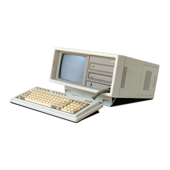
- Page 4 Chapter 1. Operating and Performance Specifications Chapter 1.0 Introduction This chapter contains operating and performance specifications for the COMPAQ PORTABLE II Personal Computer. Chapter 1.1 System Unit Table 1-1. Electrical and Mechanical Specifications ============================================================================== Dimensions: Height Depth Width ------------------------------------------------------------------------------ Weight ------------------------------------------------------------------------------ Power Requirements: Voltage...
- Page 5 ============================================================================== Chapter 1.2 Keyboard Table 1-2. Keyboard Specifications ============================================================================== Dimensions: Height Depth Width Number of Keys Keyboard: Cable Length Coil Diameter Coil Length ============================================================================== Chapter 1.3 Video Display Unit Table 1-3. Video Display Unit Specifications ============================================================================== Display Display Size Graphic Resolution Text Resolution ============================================================================== Chapter 1.4 10 Megabyte Fixed Disk Drive...
- Page 6 Data Transfer Rate Type ============================================================================== Chapter 1.5 20 Megabyte Fixed Disk Drive Table 1-5. 20 Megabyte Fixed Disk Drive Specifications ============================================================================== Dimensions: Height Depth Width Weight Media: Number of Data Heads Number of Cylinders Average Access Time Data Transfer Rate Type ============================================================================== Chapter 1.6 360 KByte Diskette Drive...
- Page 7 Tracks per Inch Number of Tracks Data Transfer Rate ============================================================================== Chapter 1.8 1.44 Megabyte Diskette Drive Specifications Table 1-8. 1.44 Megabyte Diskette Drive Specifications ============================================================================== Dimensions: Height Depth Width Weight Media: Tracks per Inch Number of Tracks Data Transfer Rate ============================================================================== Chapter 1.9 Power Supply Table 1-9.
- Page 8 Chapter 2. Power On Self Test/Problem Isolation 2.1 Power On Self Test The Power On Self Test (POST) is a series of diagnostic tests performed automatically when the system is turned on. computer system is operating properly. code appears on the screen. To start POST, follow these steps.
- Page 9 NO: Replace the AC power fuse (refer to Chapter 7 in this guide for AC power fuse removal and replacement information). steps 1 and 2. Did you hear an audible beep or see an error code on the screen? YES: See Chapter 5, "Error Messages and Codes" for information on how to identify and correct either audible or error code related problems.
- Page 10 controller board. If a color graphics or composite video monitor is not available, replace the video display controller board. If a color graphics or composite video monitor is not available and replacing the video display controller board does not solve the problem, replace the internal video display unit.
- Page 11 Chapter 3. Setup Please consult the SUPPORT SOFTWARE MAINTENANCE AND SERVICE GUIDE for current information on SETUP.
- Page 12 Chapter 4. Diagnostic Procedures Please consult the SUPPORT SOFTWARE MAINTENANCE AND SERVICE GUIDE for current information on DIAGNOSTICS.
- Page 13 Chapter 5. Error Messages and Codes 5.0 Introduction This section contains Power On Self Test (POST) messages, DIAGNOSTIC error codes, and memory error codes. that list the message or error code, a description of the error, the probable cause of the error, and the action required to resolve the error condition. Chapter 5.1 Power On Self Test Messages An error message results if a problem is encountered during the Power On Self Test.
- Page 14 XX000B YYZZ 201 - None Memory Error ------------------------------------------------------------------------------ 301 - Keyboard Error None ------------------------------------------------------------------------------ 303 - Keyboard None Controller Error ------------------------------------------------------------------------------ 304 - Keyboard or None System Unit Error ------------------------------------------------------------------------------ 401 - Printer None Interface Error ------------------------------------------------------------------------------ 402 - Monochrome 1 Long, Display Controller 2 Short...
- Page 15 DIAGNOSTICS error codes occur if the system recognizes a problem while running the DIAGNOSTICS program. defective subassemblies. Table 5-2 through 5-12 list possible error codes, a description of the error condition, and the action required to correct the condition. In each case, the Recommended Action column lists steps necessary to correct the problem.
- Page 16 Codes Error Description ------------------------------------------------------------------------------ 102 - 10 Numeric coprocessor real number calculation test failed 102 - 11 Numeric coprocessor speed test failed 102 - 12 Numeric coprocessor pattern test failed 102 - 15 Numeric coprocessor inoperative or socket unoccupied ------------------------------------------------------------------------------ 103 - 01 DMA page registers test failed 103 - 02...
- Page 17 107 - 01 CMOS RAM test failed 108 - 02 CMOS interrupt test failed ------------------------------------------------------------------------------ Error Codes Error Description ------------------------------------------------------------------------------ 108 - 03 CMOS interrupt test, CMOS not properly initialized 109 - 01 CMOS clock load data test failed. 109 - 02 CMOS clock rollover test failed 109 - 03 CMOS clock test, CMOS not properly...
- Page 18 114 - 01 Speaker test failed ============================================================================== Table 5-3. Memory Test Error Codes ============================================================================== Error Codes Error Description ------------------------------------------------------------------------------ 201 - 01 Memory machine ID test failed 201 - 02 Memory machine type test failed 201 - 03 Memory machine ID and type tests failed 202 - 01 Memory system ROM checksum failed...
- Page 19 208 - 02 Error during saving program memory in refresh test 208 - 03 Error during restore program memory in refresh test 210 - xx Incrementing pattern test failed (expanded memory test) 210 - 01 Data read from block did not match data written 210 - 02 Scan of test block prior to testing...
- Page 20 303 - 02 Keyboard LED test, reset test failed 303 - 03 Keyboard LED test, reset test failed 303 - 04 Keyboard LED test, LED command test failed 303 - 05 Keyboard LED test, LED command test failed 303 - 06 Keyboard LED test, LED command test failed 303 - 07...
- Page 21 402 - 07 Printer loopback, data, and control registers failed 402 - 08 Printer interrupt test failed 402 - 09 Printer interrupt and data register failed 402 - 10 Printer interrupt and control register failed 402 - 11 Printer interrupt, data, and control register failed 402 - 12 Printer interrupt and loopback failed...
- Page 22 509 - 01 Video 320 x 200 mode color set 1 test failed 510 - 01 Video 640 x 200 mode test failed 511 - 01 Video screen memory page test failed 512 - 01 Video gray scale test failed 514 - 0l Video white screen test failed 516 - 01...
- Page 23 614 - 02 Exceeded maximum hard error limit 614 - 03 Previously exceeded maximum soft error limit 614 - 04 Previously exceeded maximum hard error limit ------------------------------------------------------------------------------ Error Codes Error Description ------------------------------------------------------------------------------ 614 - 05 Failed to reset controller 614 - 06 Fatal error while reading 614 - 07 Fatal error while writing...
- Page 24 ------------------------------------------------------------------------------ 699 - 00 Diskette drive/media ID error ============================================================================== Table 5-8. Serial Interface Test Error Codes ============================================================================== Error Codes Error Description ------------------------------------------------------------------------------ 1101 - 01 Serial port test, UART DLAB bit failure 1101 - 02 Serial port test, line input or UART fault 1101 - 03 Serial port test, address line fault...
- Page 25 1101 - 14 Serial port test, DRIVER/RECEIVER data failure ------------------------------------------------------------------------------ 1102 - 58 Serial Port COM1 set to INTR 3 1102 - 60 Serial Port COM2 set to INTR 4 1102 - 64 Serial Port data compare error 1102 - 72 Serial Port no TX RDY 1102 - 88 Serial Port no RX RDY...
- Page 26 1201 - 16 Modem ROM, checksum failure 1201 - 17 Tone detection failure 1202 - xx Modem Internal Loopback test 1202 - 01 Timed out waiting for SYNC (local loopback mode) 1202 - 02 Timed out waiting for modem response (local loopback mode) 1202 - 03 Exceeded data block retry limit...
- Page 27 1210 - 05 XMIT exceeded carrier lost limit 1210 - 06 Timed out waiting for dial tone 1210 - 07 Dial number string too long ------------------------------------------------------------------------------ Error Codes Error Description ------------------------------------------------------------------------------ 1210 - 08 Modem timed out waiting for remote response 1210 - 09 Modem exceeded maximum redial limit...
- Page 28 1704 - xx Fixed disk drive random seek test failed 1705 - xx Fixed disk drive controller test failed 1706 - xx Fixed disk drive ready test failed 1707 - xx Fixed disk drive recalibrate test failed 1708 - xx Fixed disk drive format bad track test failed 1709 - xx...
- Page 29 17yy - 4l Drive not ready 17yy - 42 Recalibration failed ------------------------------------------------------------------------------ Error Codes Error Description ------------------------------------------------------------------------------ 17yy - 43 Failed to format bad track 17yy - 44 Failed fixed disk drive controller board diagnostics 17yy - 45 Failed to get drive parameters from 17yy - 46 Invalid drive parameters found in ROM 17yy - 47...
- Page 30 17yy - 63 Failed soft error rate 17yy - 65 Exceeded maximum bad sector per track 17yy - 66 Failed initial drive parameter 17yy - 67 Failed to write long 17yy - 68 Failed to read long 17yy - 69 Failed to read drive size from controller 17yy - 70...
- Page 31 ------------------------------------------------------------------------------ Error Codes Error Description ------------------------------------------------------------------------------ 2417 - 01 Lightpen text mode failed - no response 2417 - 02 Lightpen text mode test failed - invalid response 2417 - 03 Lightpen medium resolution mode test failed - no response 2417 - 04 Lightpen medium resolution mode test failed - invalid response ------------------------------------------------------------------------------...
- Page 32 8601 - 07 Right block not selected 8601 - 08 Timeout occurred 8601 - 10 Pointing device inoperative ============================================================================== Chapter 5.3 Memory Related Error Codes Memory error codes result when the system detects a memory fault during the Power On Self Test or diagnostic test. the memory fault to a specific chip, then generate a memory error code that identifies the defective memory chip.
- Page 33 Defective Memory Chip Isolation Map for System Boards using 64K RAMs and 256K RAMs Memory error codes are in the format XX000B YYZZ. XX is the memory segment of detected error. 000 is always equal to 000 (not used) B Byte bank location (Low: B = 0, High: B = 1)
- Page 34 XX or YY location. Figures 5-1 and 5-2 show the memory chip locations for the COMPAQ PORTABLE II Personal Computer System Boards - Version 1 and 2.
- Page 35 ============================================================================== Table 5-15. Version 2 System Board using 64K RAMs (0 - 256 Kbytes) ============================================================================== XX = 00 (Bank 0) ------------------------------------------------------------------------------ Data Bit B = 0 YY or ZZ ----------------------------------------------------------------------------- ------------------------------------------------------------------------------ XX = 02 (Bank 1) ------------------------------------------------------------------------------ Data Bit B = 0 YY or ZZ ------------------------------------------------------------------------------ ==============================================================================...
- Page 36 ============================================================================== XX = 00, 02, 04, 06 (Bank 0) ------------------------------------------------------------------------------ Data Bit B = 0 YY or ZZ ------------------------------------------------------------------------------ ------------------------------------------------------------------------------ XX = 08 (Bank 1) ------------------------------------------------------------------------------ Data Bit B = 0 YY or ZZ ------------------------------------------------------------------------------ ============================================================================== Table 5-17. Version 2 System Board using 256K RAMs (0 - 640 Kbytes) ============================================================================== XX = 00, 02, 04, 06 (Bank 0) ------------------------------------------------------------------------------...
- Page 37 ------------------------------------------------------------------------------ XX = 08 (Bank 1) ------------------------------------------------------------------------------ Data Bit B = 0 YY or ZZ ------------------------------------------------------------------------------ ============================================================================== Defective Memory Chip Isolation Map for the 512/1536 Kbyte System Memory Board Mapped into the 1 to 2.5 Megabyte Memory Space (256K x 1 Bit RAMs) NOTE: This isolation map is valid for a system memory board that uses 256K x 1 bit RAMs.
- Page 38 refer to Chapter 7. Table 5-18. Memory Locations/Required Action for 512/1536 Kbyte System Memory Board Mapped to the 1 to 2.5 Megabyte Memory Space (256K x 1 Bit RAMs) ============================================================================== XX = 10, 12, 14, 16 (Bank 2) ------------------------------------------------------------------------------ Data Bit B = 0 YY or ZZ ------------------------------------------------------------------------------...
- Page 39 ------------------------------------------------------------------------------ XX = 20, 22, 24, 26 (Bank 4) ------------------------------------------------------------------------------ Data Bit B = 0 YY or ZZ ------------------------------------------------------------------------------ ============================================================================== Replace memory chip Replace memory chip Replace memory chip Replace memory chip Replace memory chip Replace memory chip Replace memory chip Replace memory chip B = 1 High...
- Page 40 Chapter 6. Illustrated Parts Catalog 6.0 Introduction This section provides a spare parts reference for the COMPAQ PORTABLE II Personal Computer. Each table in this section contains the following information: Item - reference number keyed to an illustration. Part Number - to be used when ordering parts from Compaq Computer Corporation.
- Page 41 107678-001 --------------------------------------------------------------------------- ** Part number no longer available. ============================================================================== Chapter 6.2 Chassis Table 6-2. COMPAQ PORTABLE II Personal Computer Chassis ============================================================================== Item Part Number ------------------------------------------------------------------------------ 107899-001 ** 104081-001 ** 104198-001 ** 104059-001 ** 104050-001 101155-001 102930-001 100228-002 ** ------------------------------------------------------------------------------ * Contained in the Miscellaneous Hardware Kit (Spare PN 104270-001 **).
- Page 42 ** Part number no longer available. ============================================================================== Chapter 6.3 Common Chassis Table 6-3. COMPAQ PORTABLE II Personal Computer Common Chassis ============================================================================== Item Part Number Description...
- Page 43 ------------------------------------------------------------------------------ 104180-001 ** 104178-001 ** 104273-001 ** 106886-001 104174-001 102705-001 ** 109196-001 ** 106686-001 101340-001 ** 105033-001 ** 100025-001 ** 104067-001 ** 112693-001 (replaced by 197458-001) 104081-001 ** 104185-001 ** ------------------------------------------------------------------------------ * Contained in the Miscellaneous Hardware Kit (Spare PN 104270-001 **). See Table 6-7.
- Page 44 104176-001 ** 104186-001 ** 104008-002 104185-001 ** 104048-001 ** ------------------------------------------------------------------------------ * Contained in the Miscellaneous Hardware Kit (Spare PN 104270-001 **). See Table 6-7. Contained in the Cable Kit, Spare PN 104191-001 **. See Table 6-6. ** Part number no longer available. *** Part number 104405-001 was replaced by 142365-001.
- Page 45 Chapter 6.4 Mechanical Chassis Table 6-4. COMPAQ PORTABLE II Personal Computer Mechanical Chassis ============================================================================== Item Part Number ------------------------------------------------------------------------------ 104052-001 ** 104079-001 ** 130770-001 ** 104081-001 ** 104098-001 ** 104099-001 ** ------------------------------------------------------------------------------ * Contained in Miscellaneous Hardware Kit, Spare PN 104270-001 **.
- Page 46 Included in the Miscellaneous Hardware Kit, Spare PN 104270-001 (No longer available). Refer to Table 6-7. ============================================================================== Chapter 6.6 Cable Kit Table 6-6. COMPAQ PORTABLE II Personal Computer Cable Kit (PN 104191-001 (No longer available)) ============================================================================== Description ------------------------------------------------------------------------------ Diskette Drive Power Cable...
- Page 47 Speaker/Potentiometer Cable Diskette Drive Signal Cable Fixed Disk Drive Power Cable ============================================================================== Chapter 6.7 Miscellaneous Hardware Kit Table 6-7. COMPAQ PORTABLE II Personal Computer Miscellaneous Hardware Kit (PN 104270-001 (No longer available)) ============================================================================== Description ------------------------------------------------------------------------------ Monitor/Drive Enclosure Screw Screw Covers...
- Page 48 Chapter 7. Removal and Replacement Procedures 7.1 Preparation Before beginning the procedures in this section, complete the following steps: Turn off the computer. Close the keyboard and secure it by sliding the latches to the LOCK position (Figure 7-1) and folding the keyboard feet in place. Disconnect any peripheral devices (printers, monitors, and so on) from the computer.
- Page 49 Chapter 7.2 AC Power Fuse To remove the AC power fuse, complete the following steps: Complete the preparation procedures (see Section 7.1). Slide open the AC power compartment to expose the line filter ON/OFF switch (Figure 7-3).
- Page 50 Insert a flat bladed screwdriver along the bottom edge of the fuse box. Lift outward with enough pressure to force the fuse box out of the casing (Figure 7-4). When the fuse box is removed, locate the spare fuse provided in the holding area in the fuse box (Figure 7-5).
- Page 51 Chapter 7.3 Outer Access Casing To remove the outer access casing from the computer, complete the following steps: Complete the preparation procedure (see Section 7.1). Place the computer keyboard side down on a level work surface. the AC power access panel and the peripheral connector access panels. Using a Torx screwdriver, remove the mounting screws from the AC power and peripheral connector access areas (Figures 7-6 and 7-7).
- Page 52 Remove the outer access casing by grasping it close to the AC power and peripheral connector access panels and sliding the cover towards you. Slide it completely off the system chassis (Figure 7-8) and set it aside. NOTE: The outer access casing is flexible and will bend as needed.
- Page 53 To replace the outer access casing, reverse steps 2 and 3. Chapter 7.4 Keyboard Assembly To remove the keyboard assembly, complete the following steps: Remove the cable tray access plate (see Section 7.13). Disconnect the keyboard cable connector from the J116 socket connector on the system board (Figure 7-9).
- Page 54 Lower the rear portion of the computer so that it rests flatly against the work surface (Figure 7-10). Unlock the keyboard latches and gently slide the keyboard cable from inside the computer system chassis (Figure 7-11). from the computer system chassis. Remove the keyboard...
- Page 55 To replace the keyboard assembly, reverse steps 1 through 4. Chapter 7.5 Front Bezel To remove the front bezel, complete the following steps: Remove the keyboard assembly (see Section 7.4). Remove the brightness control knob by gently pulling it from the front bezel (Figure 7-12).
- Page 56 Lift the rear portion of the computer so that it rests firmly on the front bezel (Figure 7-13). Using a Torx screwdriver, remove the six screws that secure the front bezel to the system chassis (Figure 7-14).
- Page 57 Lower the system chassis and gently pull the front bezel from the system chassis (Figure 7-15). To replace the front bezel, reverse steps 1 through 5. Chapter 7.6 Power Supply Subassembly Chassis The power supply subassembly chassis consists of the following assemblies:...
- Page 58 Line filter ON/OFF switch assembly Power supply assembly board Power supply insulating paper To remove the power supply subassembly chassis, complete the following steps: Remove the outer access casing (see Section 7.3). Place the computer on its side (see Figure 7-16). Using a Torx screwdriver, loosen (DO NOT REMOVE) the nine mounting screws that secure the power supply chassis to the system chassis (Figure 7-17).
- Page 59 Remove only the two screws indicated in Figure 7-18.
- Page 60 Remove the power supply subassembly chassis by lifting the rear portion of the chassis upward. As this end is raised, lift the front portion of the chassis until the entire power supply chassis is free of the system chassis (Figure 7-19). NOTE: Because the power supply connects directly to the system board, be careful when removing the power supply subassembly chassis.
- Page 61 computer system chassis, disconnect the fan assembly and the automatic power switching board (Figure 7-20). Gently lift and remove the power supply subassembly from the system chassis. To replace the power supply subassembly chassis, reverse steps 1 through 6. Chapter 7.7 Fan Assembly To remove the fan assembly, complete the following steps: Remove the power supply subassembly chassis (see Section 7.6).
- Page 62 To replace the fan assembly, reverse steps 1 through 3. Chapter 7.8 Automatic Power Switching Board (APS) Remove the power supply subassembly chassis (see Section 7.6). NOTE: Carefully remove all three connections to the APS board when removing the power supply chassis. illustration of the APS board.
- Page 63 To remove the APS board, which is secured to the system chassis by four PCB standoffs, press the top of each PCB standoff together, one at a time. At the same time, carefully lift that portion of the APS board from the system chassis.
- Page 64 Slide the APS Board into place on the system Press the four PCB standoffs into the holes in the board. Hold the power supply subassembly at a 30 to 45 degree angle as shown in Figure 7-24, and tie the three wire harnesses together with a ty-wrap. >>>>>>>>>>>>>>>>>>>>>>>>>>>>>>>>>>>>>>><<<<<<<<<<<<<<<<<<<<<<<<<<<<<<<<<<<<<<<...
- Page 65 Using a Torx screwdriver, loosen (DO NOT REMOVE) the 11 mounting screws that secure the high voltage monitor access plate to the system chassis. Remove only the three mounting screws indicated in Figure 7-25. Gently slide the high voltage access plate towards the power supply chassis assembly and lift it up and away from the system chassis.
- Page 66 Gently slide the board slots access plate to the right of the computer and lift it up and away from the system chassis. To replace the board slots access plate, reverse steps 1 through 3. Chapter 7.11 Mass Storage Device Access Plate The mass storage device access plate is located at the front of the system chassis and covers all installed mass storage devices.
- Page 67 Carefully lift the mass storage device access plate away from the system chassis. To replace the mass storage device access plate, reverse steps 1 through 3. Chapter 7.12 System Memory Board Access Plate To remove the system memory board access plate, complete the following steps: Remove the outer access casing (see Section 7.3).
- Page 68 Using a Torx screwdriver, loosen (DO NOT REMOVE) the seven mounting screws that secure the system memory board access plate to the system chassis. Remove only the one mounting screw indicated in Figure 7-29. Carefully lift and remove the system memory board access plate from the system chassis (Figure 7-29).
- Page 69 Chapter 7.13 Cable Tray Access Plate To remove the cable tray access plate, complete the following steps: Remove the outer access casing (see Section 7.3). Remove the system memory board access plate (see Section 7.12). Turn over the system chassis as illustrated in Figure 7-30. Using a Torx screwdriver, loosen (DO NOT REMOVE) the seven Torx screws that secure the cable tray access plate to the system chassis.
- Page 70 Carefully lift and remove the cable tray access plate from the system chassis. To replace the cable tray access plate, reverse steps 1 through 5. Chapter 7.14 Multipurpose Controller Board The Multipurpose Controller Board is located in slot J104 on the system board (Figure 7-32).
- Page 71 Remove the board slots access plate (see Section 7.10). Disconnect the mass storage device signal cable(s) as shown in Figure 7-33. NOTE: If a fixed disk drive is installed in the system chassis, you must disconnect two signal cables. Using a Torx screwdriver, remove the board retaining screw. Carefully...
- Page 72 lift the controller board up and out of the system board (Figure 7-34). To replace the Multipurpose Controller Board, reverse steps 1 through 3. Chapter 7.15 Video Display Controller Board The Video Display Controller Board is located in slot J103 on the system board (Figure 7-35).
- Page 73 To remove the Video Display Controller Board, complete the following steps: Remove the board slots access plate (see Section 7.10). Remove the retaining screw that secures the Video Display Controller Board. Then disconnect the video display signal cable (Figure 7-36). Carefully lift the board up and out of its J103 connector location on the system board (Figure 7-37).
- Page 74 To replace the Video Display Controller Board, reverse steps 1 through 3. Chapter 7.16 512/2048 KByte Memory Expansion Board The COMPAQ PORTABLE II Personal Computer may contain up to two option boards. Option boards are always installed in the back two slots of the system chassis.
- Page 75 To replace the 512/2048 Kbyte Memory Expansion Board or other option boards, reverse steps 1 through 4. Chapter 7.17 Handle To remove the handle from the computer, complete the following steps: Remove the outer access casing (see Section 7.3). Remove the board slots access plate (see Section 7.10). Remove all controller and option boards installed (see Sections 7.14 through 7.16).
- Page 76 To replace the handle, reverse steps 1 through 4. Chapter 7.18 System Board There are two versions of the system board for the COMPAQ PORTABLE II: version 1 (Assy No. 000318) and version 2 (Assy No. 000324). The two system boards differ in shape, memory chip locations, and jumper locations (Figures 7-40 and 7-41).
- Page 77 To remove either system board, complete the following steps: Remove the power supply subassembly chassis (see Section 7.6). Remove the board slots access plate (see Section 7.10). Remove all controller and option boards installed (see Sections 7.14 through 7.16). Using Figure 7-42 as a reference, disconnect the mass storage device power cable.
- Page 78 Remove the system memory board access plate (see Section 7.12). Remove the cable tray access plate (see Section 7.13). Using Figure 7-43 as a reference, disconnect the keyboard power cable, the video display unit power cable, and the speaker/brightness control cable.
- Page 79 Using a Torx screwdriver, remove the eight mounting screws that secure the system board to the system chassis. 9. Carefully lift the system board from the System chassis (Figure 7-44). To replace the system board, reverse steps 1 through 9. If replacing a Version 1 board with a Version 2 board, the speaker/brightness potentiometer assembly (PN 104185-001 no longer available) should be replaced with an assembly containing a longer wiring...
- Page 80 Remove the 512/1536 Kbyte System Memory Board access plate (see Section 7.12). The battery is secured to the bottom of the system board by a snap in connector and cable tie. cable tie then lifting the battery from its snap in connector (Figure 7-45).
- Page 81 To replace the memory board, reverse steps 1 through 4. Chapter 7.21 Memory Option COMPAQ PORTABLE II Personal Computer memory chips can be installed on the system board, the 512/2048 Kbyte Memory Expansion Board, or the 512/1536 Kbyte System Memory Board.
- Page 82 For the system board removal and replacement procedure refer to Section 7.18. For the 512/1536 Kbyte System Memory Board removal and replacement procedure, refer to Section 7.20. NOTE: The RAM and ROM chip locations on the system boards differ from those on the memory boards (See Figures 7-47 through 7-50).
- Page 84 Using an IC removal tool, remove the defective RAM or ROM chip(s) (Figure 7-51). Using a special IC insertion tool, replace the defective RAM or ROM chip(s) (Figure 7-52).
- Page 85 (Please consult the SUPPORT SOFTWARE MAINTENANCE AND SERVICE GUIDE for current information on DIAGNOSTICS.) Chapter 7.22 Mass Storage Device Subassembly Mass storage device subassemblies for the COMPAQ PORTABLE II Personal Computer consist of fixed disk drives and diskette drives. Refer to...
- Page 86 Mass Storage Device Subassembly Enclosure To remove the mass storage device subassembly enclosure, complete the following steps: Remove the outer access casing (see Section 7.3). Remove all installed controller and option boards (see Sections 7.14 through 7.16). Using a screwdriver, gently pry the drive bezel from the front bezel (Figure 7-54).
- Page 87 Using a Torx screwdriver, remove the two screws on the right side of the system chassis and the four screws on the top of the mass storage device enclosure. These screws secure the mass storage device subassembly enclosure to the system chassis (Figure 7-55). Slide the mass storage device subassembly enclosure forward a few inches by reaching into the open system chassis area and pushing the enclosure forward.
- Page 88 Disconnect the diskette drive and fixed disk drive power cable from the system board (Figure 7-57). Grasp the sides of the mass storage device subassembly enclosure firmly and slide the enclosure out of the system chassis (Figure 7-58).
- Page 89 To replace the mass storage device subassembly enclosure, reverse steps 1 through 7. Fixed Disk Drive To remove the fixed disk drive assembly: Remove the mass storage device subassembly enclosure (see Section 7.22). Using a Torx screwdriver, remove the two shoulder bolts and vibration isolators from either side of the mass storage device subassembly enclosure.
- Page 90 NOTE: The fixed disk drive is mounted above the diskette drive. To replace the fixed disk drive assembly, reverse steps 1 and 2. Diskette Drive To remove the diskette drive assembly, complete the following steps: Remove the mass storage device subassembly enclosure (see Section 7.22).
- Page 91 NOTE: When removing the diskette drive, make sure the vibration isolators are not lost. You need to reinstall all four isolators when replacing the diskette drive assembly. To replace the diskette drive assembly, reverse steps 1 through 3. NOTE: When replacing a flip door style diskette drive with a push button style diskette drive, you should also order a replacement drive bezel (PN 104059-001 (No longer available)) to provide a better fit for the new diskette drive assembly.
- Page 92 Remove the brightness potentiometer by first unscrewing the nut that secures it to the system chassis, then push the brightness potentiometer out of the system chassis (Figure 7-62). To replace the speaker and the brightness potentiometer, reverse steps 1 through 5. Chapter 7.24 Video Display Unit...
- Page 93 To remove the video display unit (VDU), complete the following steps: Remove the keyboard assembly (see Section 7.4). Disconnect the VDU power cable (Figure 7-63). Lower the computer so that it appears as illustrated Figure 7-64.
- Page 94 Remove the high voltage access plate (see Section 7.9). Remove the front bezel (see Section 7.5) Disconnect the VDU signal cable from the VDU (Figure 7-65). The VDU high voltage cable is secured to the system chassis by a push mount with a snap connector at the end. high voltage cable by first unsnapping the push mount and then removing the cable from its place inside the connector (Figure 7-66).
- Page 95 The VDU sweep board is secured to the system chassis by five PCB stand off mounts and one screw. screw in the upper left corner of the VDU sweep board. sweep, grasp the board and gently slide it upward until the standoffs clear the mounting holes.
- Page 96 Remove the VDU from the system chassis by grasping the display screen and the VDU sweep board and then sliding the unit until it is out of the system chassis (Figure 7-69). If replacement is necessary, this unit may be shipped back to Compaq Computer Corporation packed only in a Compaq Spare VDU box.
- Page 97 To replace the video display unit, reverse steps 1 through 10. NOTE: When replacing the VDU assembly, replace the two top front mounting screws first. This helps align the screen correctly. >>>>>>>>>>>>>>>>>>>>>>>>>>>>>>>>>>>>>>><<<<<<<<<<<<<<<<<<<<<<<<<<<<<<<<<<<<<<< CAUTION The video display unit is fragile; be careful when handling it. Be careful not to disturb the VDU adjustment potentiometers on the VDU sweep board and not to break the display tube.
- Page 98 Chapter 8. Jumper Settings, Switch Settings, and Adjustments 8.1 System Board Jumper Settings Figure 8-1 shows the jumper locations on the COMPAQ PORTABLE II Version 1 system board. Refer to Table 8-1 when setting the jumpers on this board. Figure 8-2 shows the jumper locations on the COMPAQ PORTABLE II Version 2 system board.
- Page 99 Table 8-1. System Board Jumper Settings ============================================================================== Jumper Location Function ------------------------------------------------------------------------------ Video Display Unit selection ------------------------------------------------------------------------------ Speed selection ------------------------------------------------------------------------------ Reserved ------------------------------------------------------------------------------ MS1, MS2 System board memory selection ------------------------------------------------------------------------------ Memory Board 512/1536 Kbyte memory selection ============================================================================== Chapter 8.2 512/2048 KByte Memory Expansion Board Jumper Settings The jumper settings on the 512/2048 Kbyte Memory Expansion Board correspond to the amount of random access memory installed in the four banks on the option board.
- Page 100 Refer to Tables 8-2 and 8-3 when setting the jumpers on the 512/2048 Kbyte Memory Expansion Board. Table 8-2. 512/2048 Kbyte Memory Expansion Board Jumper Settings ============================================================================== Settings ------------------------------------------------------------------------------ E1 to E2, E5 to E6 E1 to E2, E4 to E5 ------------------------------------------------------------------------------ * Memory address range is dependent on system memory board configuration.
- Page 101 Banks 1,2 and 3 Banks 1, 2, 3, and 4 ============================================================================== Chapter 8.3 360 KByte Diskette Drive Switch Settings Figure 8-4 shows the COMPAQ PORTABLE II 360 Kbyte Diskette Drive. diskette drive contains an 8 position switch. setting switch positions. Table 8-4.
- Page 102 ============================================================================== Chapter 8.4 Multipurpose Controller Board Switch Settings Figures 8-5 through 8-9 show the switch and jumper locations on the Multipurpose Controller Boards and the Multipurpose Fixed Disk Drive Controller Boards. Refer to Tables 8-5 through 8-7 when setting the switches and jumpers.
- Page 103 Settings (Assy Nos. 000181-001, 000181-021, 000336-001, and 000336-021) ============================================================================== Jumper/Switch Setting ----------------------------------------------------------------------------- Open connectors on left Open connectors on right Open connectors on left Open connectors on right SW1-1 * SW1-2 SW1-3 ** SW1-4 ------------------------------------------------------------------------------ SW1-1 reserved on Assy No. 000181 boards. ** SW1-3 reserved on Assy No.
- Page 104 Table 8-7. Multipurpose Fixed Disk Drive Controller Boards Switch and Jumper Settings (Assy Nos. 000519 and 000815) ============================================================================== Switch Setting Function ------------------------------------------------------------------------------ SW500-1 Primary diskette and fixed disk drive address select (default) Secondary diskette and fixed disk drive address select SW500-2 Disable high speed transfer rates for systems without 1.2 megabyte diskette drive...
- Page 105 Chapter 8.5 Fixed Disk Drive Controller Board Figure 8-10 shows the jumper locations for the Fixed Disk Drive Controller Board (Assy No. WD1003IWH). Refer to Table 8-8 when setting the jumpers. Table 8-8. Fixed Disk Drive Controller Board Jumper Settings (Assy No.
- Page 106 ------------------------------------------------------------------------------ ============================================================================== Chapter 8.6 Video Display Controller Board Jumper Settings Figures 8-11 through 8-14 show the jumper locations on the Video Display Controller Board. Refer to Tables 8-9 and 8-10 when setting the jumpers. Table 8-9. Video Display Controller Board Switch and Jumper Settings (Assy Nos.
- Page 107 ------------------------------------------------------------------------------ J3/J5 RGB enable/disable (high scan) ============================================================================== Pin 1 to Pin 2 - Disables RGB and composite video Pin 2 to Pin 3 - RGB and composite video enable...
- Page 108 Chapter 8.7 Enhanced Color Graphics Board Switch and Jumper Settings Figures 8-15 and 8-16 show the switch and jumper locations on the Enhanced Color Graphics Boards. Refer to Table 8-11 when setting the switches and jumpers. Table 8-11. Enhanced Color Graphics Board Switch Settings (Assy Nos.
- Page 109 SW1 Settings (As the Only or Primary Video Display Controller Board) Monitor Type ------------------------------------------------------------------------------ COMPAQ Color, Compatible Enhanced Color or COMPAQ Dual Mode COMPAQ Color, Compatible Enhanced Color or COMPAQ Dual Mode RGBI Color or COMPAQ Dual Mode RGBI Color or COMPAQ Dual Mode COMPAQ Dual Mode COMPAQ Color, Compatible...
- Page 110 ------------------------------------------------------------------------------ Jumper JP3 ------------------------------------------------------------------------------ Pins Address Select ---- -------------- 1 - 2 3xxh (default) 2 - 3 2xxh ==============================================================================...
- Page 111 Chapter 8.8 Serial/Parallel Interface Board Switch Settings Figures 8-17 and 8-18 show the switch locations on the Serial/Parallel Interface Board. Refer to Tables 8-12 and 8-13 when setting the switches. Table 8-12. Serial/Parallel Interface Board Switch Settings (Assy No. 000570) ============================================================================== ------------------------------------------------------------------------------ ==============================================================================...
- Page 112 COMPAQ PORTABLE II Personal Computer. procedure, the following equipment is required: All tools normally required to service a COMPAQ PORTABLE II Personal Computer (see Preface) DIAGNOSTICS diskette Set of standard television adjustment tools COMPAQ PORTABLE II Personal Computer display template (PN 100686-003) The video display adjustment procedure is arranged in a step by step outline.
- Page 113 Remove the outer access casing. procedure. Place your COMPAQ PORTABLE II Personal Computer in a standard working position with the outer access casing removed (Figure 8-19). Insert the DIAGNOSTICS diskette in the COMPAQ PORTABLE II Personal Computer and load the DIAGNOSTICS program.
- Page 114 Using the label on the high voltage access plate as a guide, locate and adjust the BRITE control until the screen raster appears on the display. Check this display to make sure it is not tilted in any way (Figure 8-21.) NOTE: Do not use excessive force when making adjustments on the video display unit.
- Page 115 Using the VDU adjustment procedure contained in the DIAGNOSTICS program, fill the display screen with a character (refer to Chapter 4 in this guide for more information on the VDU alignment test screen). Using a plastic adjustment tool, turn the WIDTH adjustment potentiometer until the left and right edges of the display screen fall within the range specified on the adjustment template.
- Page 116 If the characters on your display appear too short or too tall, adjust the character height. the screen with capital Es (Figure 8-24). for more information on the VDU adjustment program. Two adjustments control the character height. height control potentiometer, which controls the height of characters in both the high and low resolution modes.
- Page 117 only while the computer is in a high resolution text mode. Figure 8-25 for the location of both control potentiometers.) NOTE: Do not use excessive force when making adjustments on the video display unit. Use the CTRL + ALT + < command to place the display in the low resolution graphics mode.
- Page 118 If the vertical linearity control does not exist on your video display unit, it is preset and controlled by the video display unit. Step 13 and 14 should be repeated after each adjustment until the character height are equal. If your display is shifted to the right or left, a horizontal display centering adjustment is necessary.
Need help?
Do you have a question about the Compaq Portable II and is the answer not in the manual?
Questions and answers