Table of Contents
Advertisement
Quick Links
www.ti.com
User's Guide
TLV3811EVM User's Guide
The TLV3811EVM is an evaluation board designed to evaluate the high-speed TLV3811 comparator. The
TLV3811EVM has layout options intended to make it simple to evaluate timing performance with different
measurement tools. The output of the TLV3811 is designed for low-voltage differential signals (LVDS) that
provide high-speed signals to interconnect devices such as FPGAs with minimal power dissipation.
1
Introduction.............................................................................................................................................................................2
1.1 Features.............................................................................................................................................................................
1.2 EVM Specifications............................................................................................................................................................
2 How to Make a TPHL Propagation Delay Measurement With Split Supplies....................................................................
Setup.............................................................................................................................................................................6
3.1 Supply Voltage...................................................................................................................................................................
3.2 Inputs.................................................................................................................................................................................
3.3
Outputs...............................................................................................................................................................................8
Guidelines...................................................................................................................................................................9
5 Schematic..............................................................................................................................................................................
6 Bill of Materials.....................................................................................................................................................................
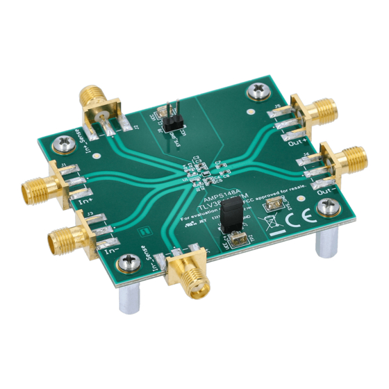
Figure 1-1. TLV3811EVM Board Top View..................................................................................................................................
Figure 1-2. TLV3811 Block Diagram............................................................................................................................................
Example..................................................................................................................................................5
Figure 3-1. TLV3811EVM Supply Voltage Connection................................................................................................................
Figure 3-3. Configuration for LVDS Inputs Using the Unused Pads of R2 and R3......................................................................
Figure 3-4. Output Side
Schematic..............................................................................................................................................8
Layers........................................................................................................................................................................9
Figure 4-2. TLV3811 EVM Block Diagram.................................................................................................................................
Figure 5-1. TLV3811 EVM Schematic........................................................................................................................................
BOM..........................................................................................................................................................................12
Trademarks
All trademarks are the property of their respective owners.
SNOU189 - MAY 2022
Submit Document Feedback
ABSTRACT
Table of Contents
List of Figures
Assignments.................................................................................................................................3
Setup...................................................................................................................4
List of Tables
Copyright © 2022 Texas Instruments Incorporated
R3...................................................................................7
Table of Contents
2
3
4
6
7
11
12
2
2
6
7
10
11
TLV3811EVM User's Guide
1
Advertisement
Table of Contents

Related Manuals for Texas Instruments TLV3811EVM


Summary of Contents for Texas Instruments TLV3811EVM
-
Page 1: Table Of Contents
The TLV3811EVM is an evaluation board designed to evaluate the high-speed TLV3811 comparator. The TLV3811EVM has layout options intended to make it simple to evaluate timing performance with different measurement tools. The output of the TLV3811 is designed for low-voltage differential signals (LVDS) that provide high-speed signals to interconnect devices such as FPGAs with minimal power dissipation. -
Page 2: Introduction
The TLV3811EVM is an evaluation board designed to evaluate the high-speed TLV3811 comparator. The TLV3811EVM has layout options intended to make it simple to evaluate timing performance with different measurement tools. The output of the TLV3811 is designed for low-voltage differential signals (LVDS) which provide high-speed signals to interconnect devices such as FPGAs with minimal power dissipation. -
Page 3: Evm Specifications
Differential Input Voltage Range: (-1.5 V to 1.5 V) Top View OUT+ OUT- Figure 1-3. TLV3811EVM Pin Assignments 1.2.1 Recommended Equipment • Dual Channel Power Supply – Using split supply operation makes it easy to measure propagation delay since the reference voltage is known to be 0V. -
Page 4: How To Make A Tphl Propagation Delay Measurement With Split Supplies
CH.4 Terminated) = -2.5V = 2.5V SENSE OUT+ OUT- Legend SENSE Matched SMA cable length SMA cable Figure 2-1. TLV3811 EVM Propagation Delay Setup TLV3811EVM User’s Guide SNOU189 – MAY 2022 Submit Document Feedback Copyright © 2022 Texas Instruments Incorporated... -
Page 5: Figure 2-2. Quick Start Example
0 V. The propagation delay was measured at approximately 206 ps with the setup described. Channel 4: OUT- Channel 1: 100mV peak-to-peak VOD 50mV VUD 50mV 10MHz Channel 3: OUT+ Figure 2-2. Quick Start Example SNOU189 – MAY 2022 TLV3811EVM User’s Guide Submit Document Feedback Copyright © 2022 Texas Instruments Incorporated... -
Page 6: Board Setup
3 Board Setup 3.1 Supply Voltage The TLV3811EVM can operate from a single supply or split supply configuration. The recommended voltage range is from 2.7-V to 5.5-V. Connect VCC, VEE, and SYS_GND using TP1, TP2, and TP3 respectively. Figure 3-1. TLV3811EVM Supply Voltage Connection TLV3811EVM User’s Guide... -
Page 7: Inputs
Additionally, the pads from R2 and R3 can be used to solder a 100-Ω termination resistor for LVDS input signals. Option for 100 differential resistor for LVDS input signals Figure 3-3. Configuration for LVDS Inputs Using the Unused Pads of R2 and R3 SNOU189 – MAY 2022 TLV3811EVM User’s Guide Submit Document Feedback Copyright © 2022 Texas Instruments Incorporated... -
Page 8: Outputs
If equipment is available to measure the LVDS output with a respect to the 100-Ω resistor or with a differential probe, then C7 and C8 can be replaced with 0-Ω resistors to keep the DC integrity of the output signal. TLV3811EVM User’s Guide SNOU189 – MAY 2022 Submit Document Feedback Copyright © 2022 Texas Instruments Incorporated... -
Page 9: Layout Guidelines
Layout Guidelines 4 Layout Guidelines Top Layer GND-1 Layer GND-2 Layer Bottom Layer Figure 4-1. Layers SNOU189 – MAY 2022 TLV3811EVM User’s Guide Submit Document Feedback Copyright © 2022 Texas Instruments Incorporated... -
Page 10: Figure 4-2. Tlv3811 Evm Block Diagram
Layout Guidelines www.ti.com IN+_SENSE 0.1uF OUT+ SYS_GND – 0.1uF OUT- ¡ SYS_GND IN-_SENSE Figure 4-2. TLV3811 EVM Block Diagram TLV3811EVM User’s Guide SNOU189 – MAY 2022 Submit Document Feedback Copyright © 2022 Texas Instruments Incorporated... -
Page 11: Schematic
Schematic 5 Schematic Figure 5-1. TLV3811 EVM Schematic SNOU189 – MAY 2022 TLV3811EVM User’s Guide Submit Document Feedback Copyright © 2022 Texas Instruments Incorporated... -
Page 12: Bill Of Materials
Fiducial mark. There is nothing to buy FID4, FID5, FID6 or mount. R2, R3 RES, 50, 0.1%, 0.5 W, 0402 0402 FC0402E50R0BTBST1 Vishay Thin Film TLV3811EVM User’s Guide SNOU189 – MAY 2022 Submit Document Feedback Copyright © 2022 Texas Instruments Incorporated... - Page 13 STANDARD TERMS FOR EVALUATION MODULES Delivery: TI delivers TI evaluation boards, kits, or modules, including any accompanying demonstration software, components, and/or documentation which may be provided together or separately (collectively, an “EVM” or “EVMs”) to the User (“User”) in accordance with the terms set forth herein.
- Page 14 www.ti.com Regulatory Notices: 3.1 United States 3.1.1 Notice applicable to EVMs not FCC-Approved: FCC NOTICE: This kit is designed to allow product developers to evaluate electronic components, circuitry, or software associated with the kit to determine whether to incorporate such items in a finished product and software developers to write software applications for use with the end product.
- Page 15 www.ti.com Concernant les EVMs avec antennes détachables Conformément à la réglementation d'Industrie Canada, le présent émetteur radio peut fonctionner avec une antenne d'un type et d'un gain maximal (ou inférieur) approuvé pour l'émetteur par Industrie Canada. Dans le but de réduire les risques de brouillage radioélectrique à...
- Page 16 www.ti.com EVM Use Restrictions and Warnings: 4.1 EVMS ARE NOT FOR USE IN FUNCTIONAL SAFETY AND/OR SAFETY CRITICAL EVALUATIONS, INCLUDING BUT NOT LIMITED TO EVALUATIONS OF LIFE SUPPORT APPLICATIONS. 4.2 User must read and apply the user guide and other available documentation provided by TI regarding the EVM prior to handling or using the EVM, including without limitation any warning or restriction notices.
- Page 17 Notwithstanding the foregoing, any judgment may be enforced in any United States or foreign court, and TI may seek injunctive relief in any United States or foreign court. Mailing Address: Texas Instruments, Post Office Box 655303, Dallas, Texas 75265 Copyright © 2019, Texas Instruments Incorporated...
- Page 18 TI products. TI’s provision of these resources does not expand or otherwise alter TI’s applicable warranties or warranty disclaimers for TI products. TI objects to and rejects any additional or different terms you may have proposed. IMPORTANT NOTICE Mailing Address: Texas Instruments, Post Office Box 655303, Dallas, Texas 75265 Copyright © 2022, Texas Instruments Incorporated...
Need help?
Do you have a question about the TLV3811EVM and is the answer not in the manual?
Questions and answers