Table of Contents
Advertisement
Quick Links
HBD-E385/E390/T39
SERVICE MANUAL
Ver. 1.0 2012.03
• HBD-E385 is the amplifi er, video, HDMI, BD/DVD/CD system, USB, LAN, wireless LAN and FM tuner section in BDV-E385.
• HBD-E390 is the amplifi er, video, HDMI, BD/DVD/CD system, USB, LAN, wireless LAN and FM tuner section in BDV-E390.
• HBD-T39 is the amplifi er, video, HDMI, BD/DVD/CD system, USB, LAN, wireless LAN and FM tuner section in BDV-T39.
Amplifier Section
BDV-E385/BDV-E390/BDV-T39
US models:
AUDIO POWER SPECIFICATIONS
POWER OUTPUT AND TOTAL HARMONIC
DISTORTION:
(FTC)
Front L + Front R:
With 3 ohms loads, both
channels driven, from 180
Hz - 20 kHz; rated 50 watts
per channel minimum
RMS power, with no more
than 1% total harmonic
distortion from 250 milli
watts to rated output.
Other models:
POWER OUTPUT (rated)
Front L/Front R:
75 W + 75 W (at 3 ohms,
1 kHz, 1% THD)
POWER OUTPUT (reference)
Front L/Front R/Surround L/Surround R:
125 W (per channel at
3 ohms, 1 kHz)
Center:
250 W (at 6 ohms, 1 kHz)
Subwoofer:
250 W (at 6 ohms, 80 Hz)
Inputs (Analog)
AUDIO (AUDIO IN)
Sensitivity: 1 V/400 mV
Inputs (Digital)
TV (Audio Return Channel/OPTICAL)
Supported formats: LPCM
2CH (up to 48 kHz), Dolby
Digital, DTS
9-890-584-01
Sony Corporation
2012C80-1
©
2012.03
Published by Sony EMCS (Malaysia) PG Tec
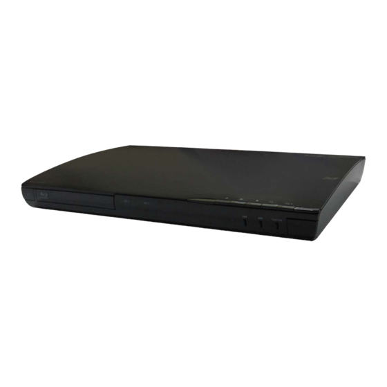
Photo: HBD-E390
SPECIFICATIONS
Video Section
Outputs
VIDEO: 1 Vp-p 75 ohms
HDMI Section
Connector
Type A (19pin)
BD/DVD/Super Audio CD/CD System
Signal format system
NTSC
USB Section
(USB) port:
Type A (For connecting
USB memory, memory
card reader, digital still
camera, and digital video
camera)
LAN Section
LAN (100) terminal
100BASE-TX Terminal
Wireless LAN Section
Blu-ray Disc/DVD receiver (HBD-E390/HBD-
E385/HBD-T39)
Standards Compliance
IEEE 802.11 b/g/n
Frequency and Channel
2.4 GHz - 2.4835 GHz
[CH1 -11]
FM Tuner Section
System
PLL quartz-locked digital
synthesizer
Tuning range
87.5 MHz - 108.0 MHz
(100 kHz step)
Antenna (aerial)
FM wire antenna (aerial)
Antenna (aerial) terminals 75 ohms, unbalanced
Canadian Model
Model Name Using Similar Mechanism
Mechanism Type
Optical Pick-up Block Name
General
Power requirements
Power consumption
BDV-E385/BDV-E390/
BDV-T39
Dimensions (approx.)
Mass (approx.)
Design and specifications are subject to change
without notice.
Standby power consumption 0.3W.
Over 85% power efficiency of amplifier block is
achieved with the full digital amplifier, S-Master.
BLU-RAY DISC/DVD RECEIVER
US Model
HBD-E385/E390/T39
HBD-E390
BDP-S390
BPX-7
KEM480AAA
120 V AC, 60 Hz
On: 130 W
Standby: 0.3 W (at the
Power Saving mode)
430 mm × 50 mm × 275
mm (17 in × 2 in ×
10
7
/
in) (w/h/d) incl.
8
projecting parts
3
2.8 kg (6 lb 2
/
oz)
4
Advertisement
Table of Contents

Subscribe to Our Youtube Channel
Related Manuals for Sony HBD-E385


Summary of Contents for Sony HBD-E385
- Page 1 Photo: HBD-E390 • HBD-E385 is the amplifi er, video, HDMI, BD/DVD/CD system, USB, LAN, wireless LAN and FM tuner section in BDV-E385. • HBD-E390 is the amplifi er, video, HDMI, BD/DVD/CD system, USB, LAN, wireless LAN and FM tuner section in BDV-E390.
- Page 2 You agree that you will use Gracenote Data, the Gracenote Software, and Gracenote Servers for • , “XMB,” and “xross media bar” are trademarks of Sony Corporation and Sony Computer your own personal non-commercial use only. You agree not to assign, copy, transfer or transmit Entertainment Inc.
- Page 3 HBD-E385/E390/T39 SAFETY CHECK-OUT After correcting the original service problem, perform the follow- ing safety check before releasing the set to the customer: Check the antenna terminals, metal trim, “metallized” knobs, screws, and all other exposed metal parts for AC leakage.
-
Page 4: Table Of Contents
HBD-E385/E390/T39 TABLE OF CONTENTS SERVICING NOTES EXPLODED VIEWS ..........6-1. Panel Section ..............79 DISASSEMBLY 6-2. Front Panel Section ............80 6-3. Chassis Bottom Section ..........81 2-1. Disassembly Flow ............12 6-4. Chassis Section ............... 82 2-2. How To Bend FFC ............13 6-5. -
Page 5: Servicing Notes
HBD-E385/E390/T39 SECTION 1 SERVICING NOTES NOTE OF REPLACING THE IC101, IC501 AND IC8001 NOTES ON HANDLING THE OPTICAL PICK-UP ON THE MB148 BOARD BLOCK OR BASE UNIT IC101, IC501 and IC8001 on the MB148 board cannot exchange with single. When these parts are damaged, exchange the complete The laser diode in the optical pick-up block may suffer electro- mounted board. - Page 6 HBD-E385/E390/T39 NOTE REPLACING OPTICAL DEVICE 1-3. Barcode decoder (BDPRdec) (KEM480AAA) OR MB148 BOARD Jig name : BDPRdec.exe Release : 2011.8.25 The password will be supplied to only service HQ, and Version : 3.0.0.0 service center name, q’ty and all of software registered...
- Page 7 HBD-E385/E390/T39 2. Pass-fail judgment of the optical device (KEM480AAA) Perform pass-fail judgment to judge whether the repair of the optical device (KEM480AAA) is necessary. 2-1. Flow of drive section check Confirm F5301 to Confirm whether Confirm whether the F5303 and F5305...
- Page 8 HBD-E385/E390/T39 3. Optical device (KEM480AAA) replacement Flow of replacement: Note: The photo in fl ow is an image. Save the text data to USB memory Barcode label on (memory capacity new optical device need not be 8GB) (KEM480AAA) bottom side...
- Page 9 HBD-E385/E390/T39 NOTE THE BD DRIVE (BPX-7) PARTS REPLACING MODEL IDENTIFICATION The mechanism blocks except optical device of BD drive (BPX-7) - Rear view - are chiefl y composed of the following parts. Part No. • HOLDER, CHUCK ASSY • LOADING ASSY •...
- Page 10 HBD-E385/E390/T39 NOTE OF REPLACING THE IC3102 AND IC3302 ON CHECKING METHOD OF NETWORK OPERATION THE AMP BOARD AND THE COMPLETE AMP BOARD It is necessary to check the network operation, when replacing the When IC3102 and IC3302 on the AMP board and the complete MB148 board.
- Page 11 HBD-E385/E390/T39 HOW TO OPEN THE TRAY WHEN POWER SWITCH TURN OFF Note 1: After the left panel is removed, this work is done. Note 2: Please prepare the thin wire (clip etc. processed to the length of 8 cm or more).
-
Page 12: Disassembly
HBD-E385/E390/T39 SECTION 2 DISASSEMBLY • This set can be disassembled in the order shown below. 2-1. DISASSEMBLY FLOW 2-2. HOW TO BEND FFC (Page 13) 2-3. LEFT PANEL, RIGHT PANEL (Page 14) 2-4. LOADING PANEL (Page 14) 2-5. TOP PANEL, FRONT PANEL ASSY (Page 15) 2-6. -
Page 13: How To Bend Ffc
HBD-E385/E390/T39 2-2. HOW TO BEND FFC : Mountain fold : Valley fold wire (flat type) (13 core), length 320 mm (Ref. No. 55) 25 mm 250 mm 35 mm MB148 board PANEL board 45º 45º (CN6303) (CN02) The upper side The upper side is contact side. -
Page 14: Left Panel, Right Panel
HBD-E385/E390/T39 Note: Follow the disassembly procedure in the numerical order given. 2-3. LEFT PANEL, RIGHT PANEL 2 nine claws 1 one screw (+BV3 (3-CR)) 4 panel, left 1 one screw (+BV3 (3-CR)) 4 panel, right 2 nine claws 2-4. LOADING PANEL... -
Page 15: Top Panel, Front Panel Assy
HBD-E385/E390/T39 2-5. TOP PANEL, FRONT PANEL ASSY 4 panel, top 1 one screw (+BV3 (3-CR)) 2 nine claws 3 Lift after doing the slide in the direction of the arrow. 6 front panel assy 5 eight claws... -
Page 16: Top Chassis, Wireless Lan Card (Wlc1), Power Key Board, Panel Board
HBD-E385/E390/T39 2-6. TOP CHASSIS, WIRELESS LAN CARD (WLC1), POWER KEY BOARD, PANEL BOARD 3 chassis, top 1 two screws (+BV3 (3-CR)) 2 seven screws (+BV3 (3-CR)) front side qa wire (flat type) (13 core) (CN02) 7 sheet, sound 8 CN603 (5P) -
Page 17: Bd Drive (Bpx-7)
HBD-E385/E390/T39 2-7. BD DRIVE (BPX-7) 3 wire (flat type) 1 flexible flat cable (45 core) (CN1101) (9 core) (CN1260) 4 four screws (+BV3 (3-CR)) 2 wire (flat type) (5 core) (CN1270) 7 BD drive BPX-7 5 boss Note: When you install the BD... -
Page 18: Switching Regulator (Swr1)
HBD-E385/E390/T39 2-9. SWITCHING REGULATOR (SWR1) 6 five screws (+BV3 (3-CR)) 1 one screw (+BV3 (3-CR)) 2 insulation, top (S) rear side 7 switching regulator (SWR1) switching regulator (SWR1) 5 CN4 (2P) 4 CN101 (4P) 3 CN1 (2P) 2-10. AMP BOARD... -
Page 19: Optical Pick-Up Block (Kem480Aaa), Wire (Flat Type)
HBD-E385/E390/T39 2-11. OPTICAL PICK-UP BLOCK (KEM480AAA), WIRE (FLAT TYPE) 3 holder, chuck assy (T) 1 four claws 2 two claws 0 insulator 6 two screws (S), float qa device, optical qf tape, FFC KEM480AAA qs tape, non-halogene qg flexible flat cable... -
Page 20: Test Mode
HBD-E385/E390/T39 SECTION 3 TEST MODE COLD RESET FACTORY INITIALIZE The cold reset clears data except BD/DVD data stored in the RAM Return all of the unit setting to their factory defaults. Note 1: Disconnect the following connections when you use this mode. - Page 21 HBD-E385/E390/T39 BD SERVICE MODE 6. The message “Close” appears, and press the [ ] button on the Note: The operation in this mode must use a remote commander and TV remote commander. monitor. Initialize Personal Information Setting method of the BD service mode: 1.
- Page 22 HBD-E385/E390/T39 2. Menu Tree Service Mode Menu Device Test Service Mode Menu [1] Dia [1] Dia [2] Lo [2] Lo [3] Factory Initialize [3] Factory Initialize [4] Network [4] Network Video Test [5] Version Up [5] Version Up Video output test...
- Page 23 HBD-E385/E390/T39 3. Service Mode Menu (Top Menu) This is the top menu of service mode. Diag Each function is accessed from this screen. Device Test Category: Operation: Moves to Diag screen Diag Moves to Log screen Moves to Factory Initialize screen...
- Page 24 HBD-E385/E390/T39 6. Diag (Audio Input Test) 8. Diag (MIC Input Test) This screen performs audio input test. This screen performs MIC input test. Note: Not used for the servicing. Screen 1: Select Audio Input Test Category 9. Diag (HDMI Input Test) Operation: This screen performs HDMI input test.
- Page 25 HBD-E385/E390/T39 12. Factory Initialize (Factory Settings) Screen 2: The IP address of the Ping point is set up (IP address input mode) There is a possibility that this mode cannot be correctly executed. When “Ping to :>” is reversed, the [ ] button is pressed and IP Never use this mode.
- Page 26 HBD-E385/E390/T39 Contents List: 16. Drive Main LSIname This menu is used to operate the drive using drive-related diagnos- Model tic and tools. Destination Sequence Number Screen 1: Selecting items under *Drive Operation: Selects the category < IFCON IFCON Version ]/[ ]...
- Page 27 HBD-E385/E390/T39 CONFIRMATION ITEM Procedure: 1. Playback Operation Confi rmation 1. Connect the router with the unit with LAN cable. 1-1. Test Disc 2. Turn on the power of the unit and the router. 3. Press the [HOME] button on the remote commander, and the Part No.
-
Page 28: Electrical Check
HBD-E385/E390/T39 SECTION 4 ELECTRICAL CHECK FM AUTO STOP CHECK generator Procedure: 1. Turn the power on. 2. Input the following signal from Signal Generator to FM an- tenna input directly. Carrier frequency : A = 87.5 MHz, B = 98 MHz, C = 108 MHz... -
Page 29: Diagrams
HBD-E385/E390/T39 SECTION 5 DIAGRAMS 5-1. BLOCK DIAGRAM - SERVO Section - BD DECODER IC101 (1/3) J6401 CN1101 (1/2) VIDEO OUT VDACX_OUT B18 RFIP RFIN CN603 USB_DP_P0 W1 WLC1 USB_DM_P0 W2 WIRELESS LAN CARD SDIO FECFREQ SCLK FEOSCEN USB WLAN VBUS... -
Page 30: Block Diagram - Memory/Hdmi Section
HBD-E385/E390/T39 5-2. BLOCK DIAGRAM - MEMORY/HDMI Section - BD DECODER IC101 (2/3) SD-RAM IC206 DQL0 - DQL7, NS_XTALO RDQ0_B - RDQ15_B X401 DQU0 - DQU7 27MHz SD-RAM NS_XTALI IC106 D1A0 - D1A13 RA0_B - RA13_B A0 - A13 DQL0 - DQL7,... -
Page 31: Block Diagram - Main Section
HBD-E385/E390/T39 5-3. BLOCK DIAGRAM - MAIN Section - DIGITAL AUDIO PROCESSOR BD DECODER IC101 (3/3) IC8001 OPTICAL OPTICAL 1 RX0/RXP0(OPT) SCL/CCLK C25 DIR_SCL RECEIVER DIGITAL IN IC5901 RX1/RXN0(ARC) SDA/CDOUT G24 DIR_SDA GPO0 H22 XDIR_INT MEMORY/HDMI GPO1 ARC_SPDIF C24 DIR_GPO3 SECTION... -
Page 32: Block Diagram - Amp Section
HBD-E385/E390/T39 5-4. BLOCK DIAGRAM - AMP Section - POWER AMP STREAM PROCESSOR IC3102 IC3001 TB3451 AMP_MCK PWM_P_1 11 MCLK 29 1N1A OUT1A FRONT L PWM_M_2 AMP_LRCK 22 LRCK IN1B OUT1A MAIN AMP_BCK 23 SCLK PWM_M_8 IN2A SECTION OVER LOAD AMP_D1... -
Page 33: Block Diagram - Power Supply Section
HBD-E385/E390/T39 5-5. BLOCK DIAGRAM - POWER SUPPLY Section - SWR1 SWITCHING REGULATOR F5304 PANEL 6V FL_6V DC FAN DRIVER IC3501 (2/2) F5301 +12V REG VOUT A+12V DCDC5V 5V VOLTAGE CONTROL DC-DC CONVERTER Q302 IC5301 F5303 FE_SW5V 3 SW UNSW12V +8V REG 8.0V... - Page 34 HBD-E385/E390/T39 THIS NOTE IS COMMON FOR PRINTED WIRING BOARDS AND SCHEMATIC DIAGRAMS. • Circuit Boards Location (In addition to this, the necessary note is printed in each block.) For Printed Wiring Boards. For Schematic Diagrams. Note: Note: • X : Parts extracted from the component side.
-
Page 35: Printed Wiring Board - Mb148 Board (Side A)
HBD-E385/E390/T39 5-6. PRINTED WIRING BOARD - MB148 Board (Side A) - • See page 34 for Circuit Boards Location. • : Uses unleaded solder. J6401 J5901 AUDIO IN VIDEO OUT CN801 MB148 LAN (100) OPTICAL FLASH BOARD CN701 DIGITAL IN... -
Page 36: Printed Wiring Board - Mb148 Board (Side B)
HBD-E385/E390/T39 5-7. PRINTED WIRING BOARD - MB148 Board (Side B) - • See page 34 for Circuit Boards Location. • : Uses unleaded solder. MB148 BOARD (SIDE B) JL6323 JL6325 JL6321 JL6327 JL6322 JL6324 JL6326 JL6320 CL5302 JL6404 JL5916 JL6403... -
Page 37: Schematic Diagram - Mb148 Board (1/9)
HBD-E385/E390/T39 5-8. SCHEMATIC DIAGRAM - MB148 Board (1/9) - • See page 61 for IC Pin Function Descriptions. MB148 BOARD (1/9) IC206 IC106 K4B2G1646C-HCH9 K4B2G1646C-HCH9 H5TQ2G63BFR-H9CR-C H5TQ2G63BFR-H9CR-C IC101 (1/12) IC206 IC106 CXD90008G-AA IC101 (2/12) SD-RAM IC101 CXD90008G-AA SD-RAM IC101 *CSP... -
Page 38: Schematic Diagram - Mb148 Board (2/9)
HBD-E385/E390/T39 5-9. SCHEMATIC DIAGRAM - MB148 Board (2/9) - • See page 55 for IC Block Diagrams. MB148 BOARD (2/9) MB148 BOARD R5354 (6/9) FAN_GND A12V (Page 42) IC5301 RT8293ALZSP CN5301 L5302 F5301 IC5301 10uH JL5313 1A 50V JL5301 F5303... -
Page 39: Schematic Diagram - Mb148 Board (3/9)
HBD-E385/E390/T39 5-10. SCHEMATIC DIAGRAM - MB148 Board (3/9) - • See page 55 for IC Block Diagrams. • See page 61 for IC Pin Function Descriptions. MB148 BOARD (4/9) (Page 40) MB148 BOARD (3/9) 3.3V IC101 (4/12) IC501 CXD90008G-AA MB148 BOARD... -
Page 40: Schematic Diagram - Mb148 Board (4/9)
HBD-E385/E390/T39 5-11. SCHEMATIC DIAGRAM - MB148 Board (4/9) - • See page 55 for IC Block Diagrams. • See page 61 for IC Pin Function Descriptions. MB148 BOARD (4/9) IC101 (5/12) CXD90008G-AA IC101 BD DECODER (VIDEO) R6416 L6402 JL6402 1.8uH... -
Page 41: Schematic Diagram - Mb148 Board (5/9)
HBD-E385/E390/T39 5-12. SCHEMATIC DIAGRAM - MB148 Board (5/9) - • See page 55 for IC Block Diagrams. • See page 61 for IC Pin Function Descriptions. MB148 BOARD (5/9) CN801 IC101 (8/12) CXD90008G-AA IC101 BD DECODER (ETHER) IC704 IC705 TK11133CSCL-G... -
Page 42: Schematic Diagram - Mb148 Board (6/9)
HBD-E385/E390/T39 5-13. SCHEMATIC DIAGRAM - MB148 Board (6/9) - • See page 53 for Waveforms. • See page 55 for IC Block Diagrams. • See page 61 for IC Pin Function Descriptions. MB148 BOARD (6/9) TH_WARN FAN_ON FAN_ON FAN_CONT FAN_CONT... -
Page 43: Schematic Diagram - Mb148 Board (7/9)
HBD-E385/E390/T39 5-14. SCHEMATIC DIAGRAM - MB148 Board (7/9) - • See page 61 for IC Pin Function Descriptions. MB148 BOARD (7/9) R1153 C1101 C1152 FE_RFO+ C1123 RFIP AVDD12_1 1.2V C1153 FE_RFO- C1122 C1102 0.001 RFIN AVDD12_2 MB148 RFIP2 FB1190 RFIN2... -
Page 44: Schematic Diagram - Mb148 Board (8/9)
HBD-E385/E390/T39 5-15. SCHEMATIC DIAGRAM - MB148 Board (8/9) - • See page 55 for IC Block Diagrams. MB148 BOARD (8/9) CN1260 FE_SLED_A- CL1266 FE_SLED_A+ CL1267 FE_SLED_B- CL1268 FE_SLED_B+ CL1269 BD DRIVE CL1265 BPX-7 FGND FE_SPDL_W CL1261 (2/3) FE_SPDL_V CL1262 FE_SPDL_U... -
Page 45: Schematic Diagram - Mb148 Board (9/9)
HBD-E385/E390/T39 5-16. SCHEMATIC DIAGRAM - MB148 Board (9/9) - • See page 53 for Waveforms. • See page 55 for IC Block Diagrams. • See page 61 for IC Pin Function Descriptions. MB148 BOARD (9/9) MB148 BOARD (4/9) IF_SDI IF_SDI... -
Page 46: Printed Wiring Board - Amp Board (Side A)
HBD-E385/E390/T39 5-17. PRINTED WIRING BOARD - AMP Board (Side A) - • See page 34 for Circuit Boards Location. • : Uses unleaded solder. SPEAKERS TB3401 TB3451 SUR L SUR R CENTER SUBWOOFER FRONT L FRONT R – – –... -
Page 47: Printed Wiring Board - Amp Board (Side B)
HBD-E385/E390/T39 5-18. PRINTED WIRING BOARD - AMP Board (Side B) - • See page 34 for Circuit Boards Location. • : Uses unleaded solder. AMP BOARD (SIDE B) JL3469 JL3470 JL3412 JL3411 C3455 JL3461 C3401 JL3465 C3457 JL3462 C3402 C3453... -
Page 48: Schematic Diagram - Amp Board (1/3)
HBD-E385/E390/T39 5-19. SCHEMATIC DIAGRAM - AMP Board (1/3) - • See page 55 for IC Block Diagrams. AMP BOARD (1/3) IC3501 BD00GC0WEFJ-SE2 IC3501 IC B/D CN3501 D3501 DC FAN DRIVER JL3504 DC-FAN + DA2J10100L JL3505 DC-FAN - (FAN) C3504 R3504 6.8k... -
Page 49: Schematic Diagram - Amp Board (2/3)
HBD-E385/E390/T39 5-20. SCHEMATIC DIAGRAM - AMP Board (2/3) - • See page 55 for IC Block Diagrams. AMP BOARD (2/3) DC_DET SL3001 PVDD_DET AMP BOARD D3503 1SS388 (1/3) R3555 (Page 48) C3552 R3556 SL3000 R3029 SL3002 47 4V C3554 0.01... -
Page 50: Schematic Diagram - Amp Board (3/3)
HBD-E385/E390/T39 5-21. SCHEMATIC DIAGRAM - AMP Board (3/3) - • See page 55 for IC Block Diagrams. SWR1 AMP BOARD AMP BOARD AMP BOARD SWITCHING REGULATOR (2/3) (2/3) (2/3) (2/3) (Page 49) (Page 49) (Page 49) 16 17 18 19... -
Page 51: 5-22. Printed Wiring Boards - Panel Section
HBD-E385/E390/T39 5-22. PRINTED WIRING BOARDS - PANEL Section - • See page 34 for Circuit Boards Location. • : Uses unleaded solder. MB148 BOARD CN6303 MB148 (Page 35) BOARD CN602 PANEL BOARD (Page 35) JR01 CL09 VOL + CL06 DC-DC CONVERTER... -
Page 52: 5-23. Schematic Diagram - Panel Section
HBD-E385/E390/T39 5-23. SCHEMATIC DIAGRAM - PANEL Section - • See page 55 for IC Block Diagrams. POWER KEY BOARD CN301 R301 CL301 PW-SW C303 S301 PW-SW "/1 CL302 PANEL BOARD ND01 VACUUM FLUORESCENT DISPLAY IC30 GP1UE27XK0VF IC30 REMOTE CONTROL CN01 3.3 3.3... -
Page 53: 5-24. Printed Wiring Board - Tuner2Fmf-Ns Board
HBD-E385/E390/T39 5-24. PRINTED WIRING BOARD - TUNER2FMF-NS Board - • Waveforms • See page 34 for Circuit Boards Location. • : Uses unleaded solder. – MB148 Board – IC5904 6 (SCKI) TUNER2FMF-NS BOARD (SIDE A) 1.54 Vp-p 40.79 ns 500 mV/DIV, 10 ns/DIV... -
Page 54: 5-25. Schematic Diagram - Tuner2Fmf-Ns Board
HBD-E385/E390/T39 5-25. SCHEMATIC DIAGRAM - TUNER2FMF-NS Board - • See page 55 for IC Block Diagrams. TUNER2FMF-NS BOARD JL128 JL126 R104 R113 10 CK C101 JL127 470p 9 LA JL121 CN101 8 IIC/RDSI JL122 JL104 7 NC ROUT IIC/RDSI MB148... - Page 55 HBD-E385/E390/T39 • IC Block Diagrams IC3001 TAS5538DGGR (AMP BOARD (1/3)) PWM_HPM_L PWM_HPP_L 56 PWM_P_6 PWM_HPM_R 55 PWM_M_6 PWM_HPP_R 54 PWM_P_5 AVSS 53 PWM_M_5 PLL_FLTM 52 VR_PWM Power Supply PLL_FLTP 51 AVSS_PWM VR_ANA 50 AVDD_PWM Digital Audio Processor PWM Section AVDD...
- Page 56 HBD-E385/E390/T39 IC3501 BD00GC0WEFJ-SE2 (AMP BOARD (1/3)) IC5302 BD00GC0WEFJ-SE2 (MB148 BOARD (2/9)) SOFT IC308 TPS54225PWPR (MB148 BOARD (2/9)) 14 VCC VO 1 UVLO 13 VIN PROTECTION LOGIC VREG5 12 VBST UNDERVOLTAGE LOCKOUT 11 SW2 REFERENCE 10 SW1 CONTROL XCON ROGIC VFB 2...
- Page 57 HBD-E385/E390/T39 IC1201 TPIC2050RDFDRG4 (MB148 BOARD (8/9)) 56 P5V_2 55 STP2_N 54 STP2_P 53 STP1_N GPOUT 52 STP1_P Charge XSLEEP 51 AGND pump SIOV 50 ISENSE Current limit 49 MCOM BEMF XSLEEP detector SPM Logic 48 ICOM2 DAC PWM On chip...
- Page 58 HBD-E385/E390/T39 IC5702 TC7WHU04FK (MB148 BOARD (5/9)) IC6303 PST8429UL (MB148 BOARD (9/9)) 4 GND GND 1 3 2A VREF 2 3Y – 1 1A VDD 2 IC5903 TC74VHC4052AFT (EK) (MB148 BOARD (6/9)) 0Y 1 2Y 2 Y-COM 3 X-COM 3Y 4...
- Page 59 HBD-E385/E390/T39 IC6401 MFI341S2162 (MB148 BOARD (4/9)) MODE1 I/O port HB/300H CPU RESET 20 NC System control 19 NC Security logic Voltage monitoring circuit 18 NC Internal address bus ROM (112 kbytes) 17 NC Internal data bus RAM (4 kbytes) 16 NC...
- Page 60 HBD-E385/E390/T39 IC101 RZ5B701-0001E2 (TUNER2FMF-NS BOARD) IISD IISD VDDRF FRF1 Digital Signal Processing FRF2 LOUT Filter Digital Stereo Mixer Demodulator Decoder GNDRF FM LNA ROUT RSSI Digital Calculation LRCK LRCK / LOUT Image Station BCLK LRCK Generator Control Detector GNDRF 7...
- Page 61 HBD-E385/E390/T39 • IC Pin Function Descriptions MB148 BOARD (1/9), (3/9), (4/9), (5/9), (6/9), (7/9) IC101 CXD90008G-AA (BD DECODER) Pin No. Pin Name Description TRINC Input of Tracking Signal (C) TRINA Input of Tracking Signal (A) FPDOCD Laser Power Monitor Input for CD APC / Differential negative input...
- Page 62 HBD-E385/E390/T39 Pin No. Pin Name Description SPBCK SPDIF input bit clock DIR_GPO2 GPIO Input of Main Beam Signal (D) Input of Main Beam Signal (C) Input of Main Beam Signal (A) FPDODVD Laser Power Monitor Input for DVD APC / Differential positive input...
- Page 63 HBD-E385/E390/T39 Pin No. Pin Name Description Input of Main Beam Signal (F) Input of Main Beam Signal (E) AVDD33_1 3.3 V Power Pin HAVC Decoupling Pin for Reference Voltage of Main and Sub Beams VDAC0 Output of General DAC RSTI...
- Page 64 HBD-E385/E390/T39 Pin No. Pin Name Description GPIO NC (PD) Not used RFIP Differential Input of AC Coupling RF SUM Signal (Positive) RFIN Differential Input of AC Coupling RF SUM Signal (Negative) NO_USE Not used NO_USE Not used NO_USE Not used...
- Page 65 HBD-E385/E390/T39 Pin No. Pin Name Description NO_USE Not used AVDD33_3 3.3 V Power Pin NO_USE Not used NO_USE Not used DVCC33_IO 3.3 V digital IO power NO_USE Not used DVCC33_IO 3.3 V digital IO power NO_USE Not used NO_USE Not used...
- Page 66 HBD-E385/E390/T39 Pin No. Pin Name Description DGND12_K Digital ground DVCC3_IO 3.3 V digital IO power DVCC12_K 1.2V digital power DGND12_K Digital ground DGND12_K Digital ground DGND12_K Digital ground DGND12_K Digital ground DGND12_K Digital ground DGND12_K Digital ground DGND12_K Digital ground DVCC12_K 1.2V digital power...
- Page 67 HBD-E385/E390/T39 Pin No. Pin Name Description NO_USE Not used DGND12_K Digital ground DGND12_K Digital ground NO_USE Not used DGND12_K Digital ground NO_USE Not used DGND12_K Digital ground DGND12_K Digital ground DVCC12_K 1.2V digital power DVCC12_K 1.2V digital power DDRVCCIO 1.5 V digital IO power DDRVCCIO 1.5 V digital IO power...
- Page 68 HBD-E385/E390/T39 Pin No. Pin Name Description DGND12_K Digital ground DGND12_K Digital ground DGND12_K Digital ground DGND12_K Digital ground DGND12_K Digital ground NO_USE Not used DVCC12_K 1.2V digital power NO_USE Not used NO_USE Not used DDRVCCIO 1.5 V digital IO power...
- Page 69 HBD-E385/E390/T39 Pin No. Pin Name Description NO_USE Not used DVCC12_K 1.2V digital power NO_USE Not used DVCC12_K 1.2V digital power DVCC12_K 1.2V digital power NO_USE Not used DVCC12_K 1.2V digital power DVCC12_K 1.2V digital power DVCC12_K 1.2V digital power NO_USE...
- Page 70 HBD-E385/E390/T39 Pin No. Pin Name Description NO_USE Not used NO_USE Not used DDRVCCIO 1.5 V digital IO power DDRVCCIO 1.5 V digital IO power NO_USE Not used DDRVCCIO 1.5 V digital IO power NO_USE Not used Memory address bit 8...
- Page 71 HBD-E385/E390/T39 Pin No. Pin Name Description AA16 NO_USE Not used AA17 NO_USE Not used AA18 NO_USE Not used AA19 DGND12_K Digital ground AA20 RA12 Memory address bit 12 AA21 AVDD33_MEMPLL 3.3 V Analog Power for MEMPLL AA22 NO_USE Not Used...
- Page 72 HBD-E385/E390/T39 Pin No. Pin Name Description AC20 RDQ7_B Memory data bit 7 AC21 RDQ5_B Memory data bit 5 AC22 RCAS_ Memory column address strobe AC23 NO_USE Not used AC24 Memory address bit 9 AC25 RRESET Memory reset NFD5 NAND Flash Data input/output bit5...
- Page 73 HBD-E385/E390/T39 MB148 BOARD (1/9) IC106, IC206 K4B2G1646C-HCH9 (SD-RAM) Pin No. Pin Name Description VDDQ DQ Power Supply: 1.5V +/-0.075V DQU5 Data Input/output: Bi-directional data bus. DQU7 Data Input/output: Bi-directional data bus. NO_USE Not used NO_USE Not used NO_USE Not used DQU4 Data Input/output: Bi-directional data bus.
- Page 74 HBD-E385/E390/T39 Pin No. Pin Name Description VDDQ DQ Power Supply: 1.5V +/-0.075V VDDQ DQ Power Supply: 1.5V +/-0.075V DQL2 Data Input/output: Bi-directional data bus. Data Strobe: Output with read data, input with write data. Edge-aligned with read data, centered in write data. For the x16, DQSL: corresponds to the data on DQL0-DQL7; DQSU corresponds to the data on DQU0-DQU7.
- Page 75 HBD-E385/E390/T39 Pin No. Pin Name Description Clock Enable: CKE HIGH activates, and CKE LOW deactivates, internal clock signal and de- vice input buffers and output drivers. Talking CKE LOW provides Precharge Power-Down and Self Refresh operation (all banks idle), or Active Power-Down (Row Active in any bank). CKE is asynchronous for self refresh exit.
- Page 76 HBD-E385/E390/T39 Pin No. Pin Name Description NO_USE Not used NO_USE Not used NO_USE Not used Address inputs: Provided the row address for active commands and the column address for Read/Write commands to select one location out of the memory array in the respective bank.
- Page 77 HBD-E385/E390/T39 MB148 BOARD (9/9) IC6301 R5F3650KCDFB (SYSTEM CONTROLLER) Pin No. Pin Name Description SIRCS_IN SIRCS signal input from the remote control receiver Fan motor speed control signal output terminal control by DA converter FAN CONT2 Port output higher, speed slower FL_D_OUT Serial data output to the fl...
- Page 78 HBD-E385/E390/T39 Pin No. Pin Name Description NO_USE No used NO_USE No used KARAOKE_MODE Karaoke mode information input terminal MIC_CLK Clock signal output terminal MIC_DATA Serial data output terminal MIC-DET_OUT Microphone detection signal output terminal Power supply terminal (+3.3V) NJU72341_POWER Power control for MIC IC...
-
Page 79: Exploded Views
HBD-E385/E390/T39 SECTION 6 EXPLODED VIEWS Note: • -XX and -X mean standardized parts, so The components identifi ed by mark 0 The components identifi ed by mark 9 con- they may have some difference from the or dotted line with mark 0 are critical for tain confi... -
Page 80: Front Panel Section
HBD-E385/E390/T39 6-2. FRONT PANEL SECTION not supplied not supplied BD drive section (BPX-7) not supplied WLC1 not supplied (POWER KEY board) not supplied chassis bottom section ND01 Note 1: When replacing the wireless LAN card (WLC1), refer to “CHECKING METHOD OF NETWORK OPERATION”... -
Page 81: Chassis Bottom Section
HBD-E385/E390/T39 6-3. CHASSIS BOTTOM SECTION not supplied not supplied not supplied not supplied not supplied chassis section Note: Wires (fl at type) for service is all straight. Please bend it referring go “HOW TO BEND FFC” on page 13 when you install it in the unit. -
Page 82: Chassis Section
HBD-E385/E390/T39 6-4. CHASSIS SECTION SWR1 not supplied not supplied not supplied Ref. No. Part No. Description Remark 3-077-331-71 +BV3 (3-CR) 4-295-590-01 FOOT 0 SWR1 1-474-368-11 SWITCHING REGULATOR (3L382W-1) -
Page 83: Bd Drive Section (Bpx-7)
HBD-E385/E390/T39 6-5. BD DRIVE SECTION (BPX-7) not supplied not supplied not supplied not supplied not supplied Note: Wires (fl at type) for service is all straight. Please bend it referring go “HOW TO BEND FFC” on page 13 when you install it in the unit. -
Page 84: Electrical Parts List
HBD-E385/E390/T39 SECTION 7 ELECTRICAL PARTS LIST Note: • Due to standardization, replacements in • SEMICONDUCTORS The components identifi ed by mark 0 the parts list may be different from the In each case, u: μ, for example: or dotted line with mark 0 are critical for parts specifi... - Page 85 HBD-E385/E390/T39 Ref. No. Part No. Description Remark Ref. No. Part No. Description Remark C3339 1-114-868-11 CERAMIC CHIP 0.1uF D3303 6-503-733-01 DI 1SMB51AT3G C3340 1-118-066-11 CERAMIC CHIP 0.1uF 100V D3304 6-503-733-01 DI 1SMB51AT3G C3341 1-118-066-11 CERAMIC CHIP 0.1uF 100V D3351 8-719-056-48...
- Page 86 HBD-E385/E390/T39 MB148 Ref. No. Part No. Description Remark Ref. No. Part No. Description Remark R3153 1-220-281-11 METAL CHIP 4.7K 1/4W R3530 1-216-295-91 SHORT CHIP R3154 1-220-281-11 METAL CHIP 4.7K 1/4W R3531 1-216-295-91 SHORT CHIP R3155 1-220-281-11 METAL CHIP 4.7K 1/4W...
- Page 87 HBD-E385/E390/T39 MB148 Ref. No. Part No. Description Remark Ref. No. Part No. Description Remark C204 1-100-916-11 CERAMIC CHIP 0.1uF C806 1-112-777-11 CERAMIC CHIP 0.01uF C206 1-100-916-11 CERAMIC CHIP 0.1uF C811 1-100-916-11 CERAMIC CHIP 0.1uF C207 1-100-916-11 CERAMIC CHIP 0.1uF C812 1-100-916-11 CERAMIC CHIP 0.1uF...
- Page 88 HBD-E385/E390/T39 MB148 Ref. No. Part No. Description Remark Ref. No. Part No. Description Remark * C5603 1-116-719-11 CERAMIC CHIP 10uF 6.3V C8005 1-112-777-11 CERAMIC CHIP 0.01uF C5604 1-114-130-11 CERAMIC CHIP 1uF 6.3V C8006 1-112-777-11 CERAMIC CHIP 0.01uF * C5605 1-116-719-11 CERAMIC CHIP 10uF 6.3V...
- Page 89 HBD-E385/E390/T39 MB148 Ref. No. Part No. Description Remark Ref. No. Part No. Description Remark IC307 6-717-879-01 IC RT8293ALZSP R207 1-208-668-11 METAL CHIP 0.5% 1/16W IC308 6-714-935-01 IC TPS54225PWPR R302 1-216-295-91 SHORT CHIP IC501 (Not supplied) IC TC58NVG1S3ETA00B3Q R327 1-218-953-11 METAL CHIP...
- Page 90 HBD-E385/E390/T39 MB148 Ref. No. Part No. Description Remark Ref. No. Part No. Description Remark R1153 1-218-965-11 METAL CHIP 1/16W R5934 1-218-973-11 METAL CHIP 1/16W R1191 1-250-512-11 METAL CHIP 5.1K 1/16W R5935 1-218-973-11 METAL CHIP 1/16W R1192 1-218-961-11 METAL CHIP 4.7K...
- Page 91 HBD-E385/E390/T39 MB148 PANEL Ref. No. Part No. Description Remark Ref. No. Part No. Description Remark R6341 1-218-941-81 METAL CHIP 1/16W < THERMISTOR > R6342 1-218-990-81 SHORT CHIP R6343 1-218-970-11 METAL CHIP 1/16W TH6301 1-804-949-11 THERMISTOR, NTC (SMD) R6347 1-218-965-11 METAL CHIP 1/16W <...
- Page 92 HBD-E385/E390/T39 PANEL POWER KEY TUNER2FMF-NS Ref. No. Part No. Description Remark Ref. No. Part No. Description Remark JR12 1-216-864-11 SHORT CHIP 1-771-410-21 SWITCH, TACTILE (VOL –) JR13 1-216-295-91 SHORT CHIP 1-771-410-21 SWITCH, TACTILE (VOL +) JR15 1-216-295-91 SHORT CHIP 1-771-410-21...
- Page 93 HBD-E385/E390/T39 TUNER2FMF-NS Ref. No. Part No. Description Remark < COIL > L103 1-481-524-11 INDUCTOR 10uH L104 1-481-521-11 INDUCTOR L105 1-481-521-11 INDUCTOR < RESISTOR > R101 1-216-809-11 METAL CHIP 1/10W R103 1-216-801-11 METAL CHIP 1/10W R104 1-216-864-11 SHORT CHIP R105 1-216-801-11...
- Page 94 HBD-E385/E390/T39 REVISION HISTORY Checking the version allows you to jump to the revised page. Also, clicking the version at the top of the revised page allows you to jump to the next revised page. Ver. Date Description of Revision 2012.03...
Need help?
Do you have a question about the HBD-E385 and is the answer not in the manual?
Questions and answers