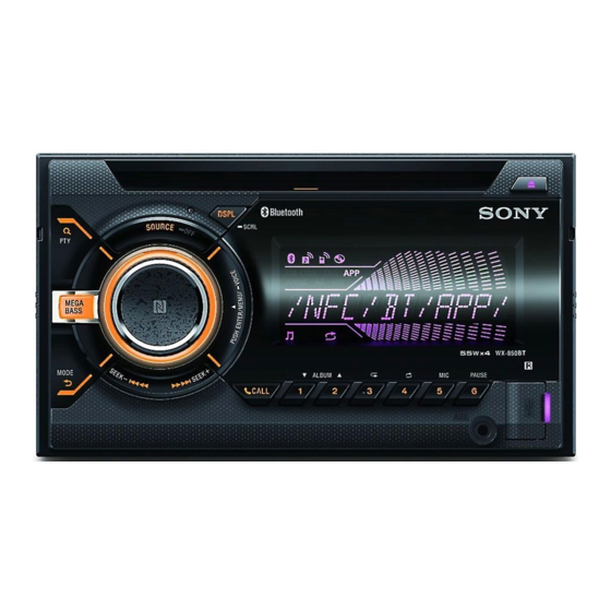
Sony WX-850BT Service Manual
Hide thumbs
Also See for WX-850BT:
- Operating instructions manual (35 pages) ,
- Operating instructions manual (108 pages)
Table of Contents
Advertisement
Quick Links
SERVICE MANUAL
Ver. 1.1 2016.02
The service manual of the mechanism deck, used in
this model, has been issued in a separate volume.
Please refer to the service manual of the MG-101
series for the mechanism deck information.
• The tuner and CD sections have no adjustments.
(US and Canadian models only)
FOR THE CUSTOMERS IN THE USA. NOT
APPLICABLE IN CANADA, INCLUDING IN THE
PROVINCE OF QUEBEC.
POUR LES CLIENTS AUX ÉTATS-UNIS. NON
APPLICABLE AU CANADA, Y COMPRIS LA
PROVINCE DE QUÉBEC.
AUDIO POWER SPECIFICATIONS
CEA2006 Standard
Power Output: 17 Watts RMS × 4 at 4
Ohms < 1% THD+N
SN Ratio: 80 dBA
(reference: 1 Watt into 4 Ohms)
Tuner section (US and Canadian models)
FM
Tuning range: 87.5 – 107.9 MHz
Antenna (aerial) terminal:
External antenna (aerial) connector
Intermediate frequency:
FM CCIR: -1,956.5 to -487.3 kHz and
+500.0 to +2,095.4 kHz
Usable sensitivity: 8 dBf
Selectivity: 75 dB at 400 kHz
Signal-to-noise ratio: 73 dB
Separation: 50 dB at 1 kHz
Frequency response: 20 – 15,000 Hz
AM
Tuning range: 530 – 1,710 kHz
Antenna (aerial) terminal:
External antenna (aerial) connector
Sensitivity: 26 μV
Tuner section (AEP and UK models)
FM
Tuning range: 87.5 – 108.0 MHz
Antenna (aerial) terminal:
External antenna (aerial) connector
Intermediate frequency:
FM CCIR: -1,956.5 to -487.3 kHz and
+500.0 to +2,095.4 kHz
Usable sensitivity: 8 dBf
Selectivity: 75 dB at 400 kHz
Signal-to-noise ratio: 73 dB
Separation: 50 dB at 1 kHz
Frequency response: 20 – 15,000 Hz
9-896-191-02
Sony Video & Sound Products Inc.
2016B33-1
©
2016.02
Published by Sony Techno Create Corporation
Photo: WX-900BT
Model Name Using Similar Mechanism
Mechanism Type
Optical Pick-up Name
SPECIFICATIONS
MW/LW
CD Player section
Tuning range:
Signal-to-noise ratio: 120 dB
MW: 531 – 1,602 kHz
Frequency response: 10 – 20,000 Hz
LW: 153 – 279 kHz
Wow and flutter: Below measurable limit
Antenna (aerial) terminal:
The maximum number of: (CD-R/CD-RW only)
External antenna (aerial) connector
–
folders (albums): 150 (including root folder)
Sensitivity: MW: 26 μV, LW: 50 μV
–
files (tracks) and folders: 300 (may less than 300
if folder/file names contain many characters)
Tuner section
–
displayable characters for a folder/file name: 32
(Joliet)/64 (Romeo)
(E, Indian and Australian models)
Corresponding codec: MP3 (.mp3), WMA (.wma)
FM
and AAC (.m4a)
Tuning range:
USB Player section
87.5 – 108.0 MHz (at 50 kHz step)
87.5 – 108.0 MHz (at 100 kHz step)
Interface: USB (High-speed)
87.5 – 107.9 MHz (at 200 kHz step)
Maximum current: 1 A
FM tuning step:
The maximum number of recognizable tracks:
50 kHz/100 kHz/200 kHz switchable
10,000
Antenna (aerial) terminal:
Corresponding codec:
External antenna (aerial) connector
MP3 (.mp3)
Intermediate frequency:
FM CCIR: -1,956.5 to -487.3 kHz and
+500.0 to +2,095.4 kHz
Usable sensitivity: 8 dBf
WMA (.wma)
Selectivity: 75 dB at 400 kHz
Signal-to-noise ratio: 73 dB
Separation: 50 dB at 1 kHz
AAC (.m4a, .mp4)
Frequency response: 20 – 15,000 Hz
AM
WAV (.wav)
Tuning range:
531 – 1,602 kHz (at 9 kHz step)
530 – 1,710 kHz (at 10 kHz step)
FLAC (.flac)
AM tuning step:
9 kHz/10 kHz switchable
Antenna (aerial) terminal:
External antenna (aerial) connector
Sensitivity: 26 μV
WX-850BT/900BT/
Australian Model
Wireless Communication
Communication System:
Output:
Maximum communication range:
Frequency band:
Modulation method: FHSS
Compatible BLUETOOTH Profiles*
Corresponding codec:
Bit rate: 8 - 320 kbps (Supports VBR (Variable
Bit Rate))
*1 The actual range will vary depending on factors such
Sampling rate: 16 - 48 kHz
Bit rate: 32 - 192 kbps (Supports VBR
(Variable Bit Rate))
*2 BLUETOOTH standard profiles indicate the purpose
Sampling rate: 32 kHz, 44.1 kHz, 48 kHz
Bit rate: 8 - 320 kbps
Power amplifier section
Sampling rate: 11.025 - 48 kHz
Output: Speaker outputs
Bit depth: 16 bit
Speaker impedance: 4 – 8 ohms
Sampling rate: 44.1 kHz, 48 kHz
Maximum power output: 55 W × 4 (at 4 ohms)
Bit depth: 16 bit, 24 bit
Sampling rate: 44.1 kHz, 48 kHz
900BTM
US Model
Canadian Model
WX-850BT/900BT
AEP Model
UK Model
E Model
WX-900BT
Indian Model
WX-900BT/900BTM
MEX-N4100BT/N4150BT
MG-101CF-188
DAX-25A
BLUETOOTH Standard version 3.0
BLUETOOTH Standard Power Class 2
(Max. +4 dBm)
Line of sight approx. 10 m (33 ft)*
1
2.4 GHz band (2.4000 – 2.4835 GHz)
2
:
A2DP (Advanced Audio Distribution Profile) 1.3
AVRCP (Audio Video Remote Control Profile) 1.5
HFP (Handsfree Profile) 1.6
PBAP (Phone Book Access Profile)
SPP (Serial Port Profile)
MAP (Message Access Profile)
HID (Human Interface Device Profile)
SBC (.sbc) and AAC (.m4a)
as obstacles between devices, magnetic fields
around a microwave oven, static electricity,
reception sensitivity, antenna (aerial)'s performance,
operating system, software application, etc.
of BLUETOOTH communication between devices.
– Continued on next page –
AUDIO SYSTEM
Advertisement
Table of Contents

Related Manuals for Sony WX-850BT


Summary of Contents for Sony WX-850BT
- Page 1 Selectivity: 75 dB at 400 kHz AUDIO SYSTEM Signal-to-noise ratio: 73 dB Separation: 50 dB at 1 kHz Frequency response: 20 – 15,000 Hz 9-896-191-02 Sony Video & Sound Products Inc. 2016B33-1 © 2016.02 Published by Sony Techno Create Corporation...
- Page 2 Bluetooth SIG, Inc. and any ground (earth)) documentation and/or other materials provided use of such marks by Sony Corporation is under Rated current consumption: 10 A with the distribution. license. Other trademarks and trade names are Dimensions: those of their respective owners.
-
Page 3: Table Of Contents
WX-850BT/900BT/900BTM SECTION 1 SERVICING NOTES TABLE OF CONTENTS The SERVICING NOTES contains important information for servicing. Be sure to read this section before repairing the SERVICING NOTES unit..........GENERAL ..............16 NOTES ON HANDLING THE OPTICAL PICK-UP BLOCK OR BASE UNIT DISASSEMBLY 3-1. - Page 4 WX-900BT: E and Australian models (E) 4-575-531-0[] WX-900BT: Indian model (IN) WX-900BTM: Indian model 4-575-532-0[] (MARUTI SUZUKI model) (IN) WX-850BT: US and Canadian models 4-588-101-0[] (Wal-Mart model) (UC) DESTINATION ABBREVIATIONS The following abbreviations for model destinations are used in this service manual.
- Page 5 WX-850BT/900BT/900BTM DESTINATION SETTING METHOD 4. The resetting operation is executed by pressing the [SOURCE OFF] button for 1 second after the setting ends, and the unit When the complete MAIN board or serial fl ash (IC502) is re- returns to the normal condition.
- Page 6 WX-850BT/900BT/900BTM Ver. 1.1 • Method of operation by remote commander 2. In the state in which the software main version is displayed on the liquid crystal display (refer to the following fi gure), (850BT, 900BT: US, Canadian, E, Indian, Australian...
- Page 7 WX-850BT/900BT/900BTM TEST DISCS CANCELING THE DEMO MODE Use following TEST DISC (for CD) when this unit confi rms the You can cancel the demonstration display which operation and checks it. appears when the source is off and the clock is displayed.
- Page 8 Bluetooth compatible smartphone or cellular phone 2. Search for the distance of this unit and the Bluetooth device • Bluetooth audio devices (SONY NWZ-A826, or select from (smartphone or cellular phone) about 5 m apart. connectable smartphone, cellular phones or audio devices list) Confi...
- Page 9 WX-850BT/900BT/900BTM BLUETOOTH INFORMATION WRITING METHOD 1. Installing the NFC Tag Data Writing Application for When the complete MAIN board or knob (VOL) assy (Ref. No. the Servicing NFC1) is replaced, the writing of Bluetooth information is neces- Install the NFC Tag Data Writing Application on the smart- sary.
- Page 10 WX-850BT/900BT/900BTM • Checking the Version of the NFC Tag Data Writing 2. Writing the NFC Tag Data Application Write the NFC tag data (Bluetooth information) to the NFC mod- ule in the knob (VOL) assy (Ref. No. NFC1). Procedure: 1. Start the NFC Tag Data Writing Application on the smart- Procedure: phone.
- Page 11 WX-850BT/900BT/900BTM How to display on the liquid crystal display by the 5. Input the Bluetooth Local Name (BL_NAME). Tap the “List” on the screen of the smartphone and select the test mode: model name of the this unit. If there is not model name of the...
- Page 12 WX-850BT/900BT/900BTM 9. Check that “Completed!” is displayed on the screen of the 16. Check that “Completed!” is displayed on the screen of the smartphone. smartphone. Note 2: When “Completed!” is not displayed on the screen of the smart- Note 3: When “Completed!” is not displayed on the screen of the smart- phone, refer to “3.
- Page 13 WX-850BT/900BT/900BTM 3. Error Display 4. Check Method of the NFC Tag Data When the writing of the NFC tag data has failed, “Error” is dis- Check the NFC tag data according to the procedure below. played on the screen of the smartphone.
- Page 14 WX-850BT/900BT/900BTM How to display on the liquid crystal display by the 5. Check that “BD_ADDR” on the screen of the smartphone ac- cords with BD_ADDR written on the BT module label and test mode: “MODE” on the screen of the smartphone is “00 00 (Read- 1 In the state of source off (the clock is displayed on the only)”.
- Page 15 WX-850BT/900BT/900BTM 5. The Factor that One Touch Connection is Impossible The four following factors are considered as the factor that one touch connection is impossible. Guess and check the defective factor by each checking result. Note: The four following factors are examples.
-
Page 16: General
WX-850BT/900BT/900BTM Ver. 1.1 SECTION 2 This section is extracted GENERAL from operating instruction. (US and Canadian models) Connection Connection/Installation Subwoofer* Cautions Run all ground (earth) leads to a common ground (earth) point. Do not get the leads trapped under a screw, or caught in moving parts (e.g., seat railing). - Page 17 Installation of the connection cable RC-SR1 (not Larger than 172 × 97 mm (6 × 3 in) (w/h), with consult your nearest Sony dealer. supplied) is required before use. an inner corner radius of less than 0.5 mm ( in).
- Page 18 WX-850BT/900BT/900BTM (AEP and UK models) Connection Connection/Installation Subwoofer* Cautions Run all ground (earth) leads to a common ground (earth) point. Do not get the leads trapped under a screw, or caught in moving parts (e.g., seat railing). Before making connections, turn the car ignition off to avoid short circuits.
- Page 19 If the fuse blows [STR CONTROL] in [SET STEERING] to again after replacement, there may be an internal malfunction. In such a case, [PRESET]. consult your nearest Sony dealer. Larger than 182 mm (7 Larger than 111 mm...
- Page 20 WX-850BT/900BT/900BTM (E, Indian and Australian models) Connection Connection/Installation Subwoofer* Cautions Run all ground (earth) leads to a common ground (earth) point. Do not get the leads trapped under a screw, or caught in moving parts (e.g., seat railing). Before making connections, turn the car ignition off to avoid short circuits.
- Page 21 If the fuse blows To enable the wired remote control, set again after replacement, there [STR CONTROL] in [SET STEERING] to may be an internal malfunction. In such a case, [PRESET]. consult your nearest Sony dealer.
-
Page 22: Disassembly
WX-850BT/900BT/900BTM SECTION 3 DISASSEMBLY • This set can be disassembled in the order shown below. 3-1. DISASSEMBLY FLOW 3-2. MINI FUSE (BLADE TYPE) (FU1), 3-7. SERVICE POSITION COVER (Page 27) (Page 22) 3-3. PANEL FRONT BLOCK (Page 23) 3-4. CD MECHANISM DECK (MG-101CF-188) 3-6. -
Page 23: Panel Front Block
WX-850BT/900BT/900BTM 3-3. PANEL FRONT BLOCK 3 connector (CN101) main block 1 two claws 2 Remove the panel front block in the direction of the arrow. 4 panel front block 1 two claws 1 two claws Note: When installing the cable flexible flat (22 core) to the connector (CN101) on the MAIN board, insert straight to the connector and lock a connector completely. -
Page 24: Cd Mechanism Deck (Mg-101Cf-188)
WX-850BT/900BT/900BTM 3-4. CD MECHANISM DECK (MG-101CF-188) Note 1: The service manual of the mechanism deck, used in this mod- el has been issued in a separate volume. Please refer to the service manual of the MG-101 series for the mechanism deck information. -
Page 25: Main Board
WX-850BT/900BT/900BTM 3-5. MAIN BOARD Note 1: When the complete MAIN board is replaced, it is necessary to replace knob (VOL) assy (Ref. No. NFC1) simultaneously. Also, the destination setting, Bluetooth operation check and Bluetooth information writing is necessary. Refer to “DESTI- NATION SETTING METHOD”... -
Page 26: Knob (Vol) Assy (Nfc1), Panel Front Assy, Key Board
WX-850BT/900BT/900BTM 3-6. KNOB (VOL) ASSY (NFC1), PANEL FRONT ASSY, KEY BOARD Note 1: When the knob (VOL) assy (Ref. No. NFC1) is replaced, Bluetooth information writing is necessary. Refer to “BLUE- TOOTH INFORMATION WRITING METHOD” on page 9. Note 2: When installing the cable flexible flat (22 core) (FFC2) to the connector (CN901) on the KEY board, insert straight to the connector and lock a connector completely. -
Page 27: Service Position
WX-850BT/900BT/900BTM SECTION 4 TEST MODE 3-7. SERVICE POSITION SETTING THE TEST MODE Setting method: Note 1: The service position below cannot be performed with the fl ex- ible fl at cable (length: 80 mm) used with the unit. Refer to 1. -
Page 28: Diagrams
WX-850BT/900BT/900BTM SECTION 5 DIAGRAMS 5-1. BLOCK DIAGRAM - SERVO/USB/Bluetooth Section - CD MECHANISM DECK BLOCK AU_FL_CH, (MG-101CF-188) AU_RL_CH, AU_SUB_CH AU_FL_CH >002B FPI1 RFRP 27 RFZI DAO3 (Page 29) 17 FPI2 DAO2 R-CH AU_RL_CH 16 FNI1 DAO4 15 FNI2 DAO1 R-CH... -
Page 29: Block Diagram - Main Section
WX-850BT/900BT/900BTM 5-2. BLOCK DIAGRAM - MAIN Section - INPUT SELECTOR, ELECTRICAL VOLUME AU_FL_CH, IC402 AU_RL_CH, J401 AU_SUB_CH AU_FL_CH >002B 33 INF1 OUTF1 FRONT (Page 28) R-CH AU_RL_CH 31 INR1 OUTR1 REAR AUDIO OUT R-CH AU_SUB_CH 30 INS OUTC R-CH OUTS... -
Page 30: Block Diagram - Panel/Power Supply Section
WX-850BT/900BT/900BTM 5-3. BLOCK DIAGRAM - PANEL/POWER SUPPLY Section - AUDIO DSP, SYSTEM CONTROLLER MUTING1 >006B IC503 (3/3) (Page 29) RESET SIGNAL 84 RC_IN1 GENERATOR J801 IC501 (REMOTE IN) 81 RC_IN0 RESET >001B S919 BUFFER (RESET) (Page 28) Q1307 +1.2V BUFFER -COM_1.2V... - Page 31 WX-850BT/900BT/900BTM THIS NOTE IS COMMON FOR PRINTED WIRING BOARDS AND SCHEMATIC DIAGRAMS. • Waveforms (In addition to this, the necessary note is printed in each block.) – MAIN Board – For Printed Wiring Boards. For Schematic Diagrams. IC001 es (XTAL_IN) IC503 <zv/ (USB_X2)
-
Page 32: Printed Wiring Boards - Main Section (1/2)
WX-850BT/900BT/900BTM Ver. 1.1 5-4. PRINTED WIRING BOARDS - MAIN Section (1/2) - • : Uses unleaded solder. MAIN BOARD (COMPONENT SIDE) C329 C332 IC801 C310 C315 D805 C807 R829 C307 R303 C811 R834 C816 C1572 C825 D809 R831 Q1302 C1573... -
Page 33: Printed Wiring Board - Main Section (2/2)
WX-850BT/900BT/900BTM Ver. 1.1 5-5. PRINTED WIRING BOARD - MAIN Section (2/2) - • : Uses unleaded solder. (900BT: US, CND) J401 CN301 (FRONT VIEW) REAR FRONT AUDIO OUT AUDIO OUT J1001 J801 AUDIO OUT (REMOTE IN) MAIN BOARD (CONDUCTOR SIDE) -
Page 34: Schematic Diagram - Main Section (1/4)
WX-850BT/900BT/900BTM 5-6. SCHEMATIC DIAGRAM - MAIN Section (1/4) - • See page 31 for Waveforms. • See page 41 for IC Block Diagrams. • See page 44 for IC Pin Function Description. MAIN BOARD (1/4) 0.22 12MHz VDR1 JL725 RSB12ZT2L... -
Page 35: Schematic Diagram - Main Section (2/4)
WX-850BT/900BT/900BTM Ver. 1.1 5-7. SCHEMATIC DIAGRAM - MAIN Section (2/4) - • See page 41 for IC Block Diagrams. (850BT/900BT: US, CND, E, IND, AUS) MAIN BOARD (2/4) IC301 REAR RCH (+) J401 REAR LCH (+) POWER AMP IC301 REAR RCH (–) PURE5001H-4WX REAR LCH (–) -
Page 36: Schematic Diagram - Main Section (3/4)
WX-850BT/900BT/900BTM Ver. 1.1 5-8. SCHEMATIC DIAGRAM - MAIN Section (3/4) - • See page 41 for IC Block Diagrams. (900BT: US, CND) CN801 MAIN BOARD (3/4) (SIRIUSXM IN) F801 R836 D809 R841 DZ2J18000L 100k D808 R834 DZ2J18000L R848 D805 DZ2J18000L... -
Page 37: Schematic Diagram - Main Section (4/4)
WX-850BT/900BT/900BTM 5-9. SCHEMATIC DIAGRAM - MAIN Section (4/4) - • See page 31 for Waveforms. • See page 41 for IC Block Diagrams. • See page 44 for IC Pin Function Description. MAIN BOARD (4/4) DEC_BCK_IN R1452 IC501 IC504 C528... -
Page 38: Key Board (Component Side)
WX-850BT/900BT/900BTM 5-10. PRINTED WIRING BOARD - KEY Board (Component Side) - • : Uses unleaded solder. S901 KEY BOARD (COMPONENT SIDE) S919 (RESET) S902 SOURCE S906 S917 DSPL SCRL LED915 LED906 LCD901 LED901, 902 LIQUID CRYSTAL DISPLAY S907 (KEY ILLUMINATION) -
Page 39: Key Board (Conductor Side)
WX-850BT/900BT/900BTM 5-11. PRINTED WIRING BOARD - KEY Board (Conductor Side) - • : Uses unleaded solder. KEY BOARD (CONDUCTOR SIDE) R980 R988 R928 R927 R982 R983 R990 R1016 R974 Q911 Q903 R985 R905 R987 Q912 R986 R916 R981 R1017 C903... -
Page 40: 5-12. Schematic Diagram - Key Board
WX-850BT/900BT/900BTM Ver. 1.1 5-12. SCHEMATIC DIAGRAM - KEY Board - • See page 41 for IC Block Diagrams. KEY BOARD R941 LED901 LED905 LED906 SMLVN6RGB1U1 SMLVN6RGB1U1 SMLVN6RGB1U1 (KEY ILLUMINATION) (KEY ILLUMINATION) (LCD BACK LIGHT) R942 LED902 LED915 SMLVN6RGB1U1 SMLVN6RGB1U1 (KEY ILLUMINATION) - Page 41 WX-850BT/900BT/900BTM • IC Block Diagrams – MAIN Board – IC001 SDP2014HN/V102 32 31 27 26 VDDA_IFADC 1 DIGITAL CONTROL DIGITAL XTAL OSCILLATION VSSA_IFADC 2 TUNING OSCILLATION SYSTEM VBGP 3 DIVIDERS FM_CAP 4 IC CONTROL UNIT FM_IN_M 5 FRONT-END FM_IN_P 6...
- Page 42 WX-850BT/900BT/900BTM IC402 BD3468FV-E2 FADER FADER BOOST LEVEL OUTC SHIFT SELECTION FADER FADER BOOST LEVEL OUTS SHIFT A1 1 A2 2 FADER FADER LEVEL OUTR1 BOOST SHIFT BP1 3 REAR SELECTION FADER FADER LEVEL OUTR2 BOOST SHIFT BP2 4 CP1 5...
- Page 43 WX-850BT/900BT/900BTM IC804 BD60HC0WEFJ-E2 IC1003 NJM2781RB1 NOISE 1 8 GND REG 2 REGULATOR STBY 3 7 V+ OVER CURRENT PROTECITON IN+ 4 6 OUT – 5 IN– SOFT – – START THERMAL SHUTDOWN IC805 S-13A1A12-E6T1U3 VOUT 1 OVERCURRENT PROTECTION THERMAL SHUTDOWN ON/OFF –...
- Page 44 WX-850BT/900BT/900BTM • IC Pin Function Description MAIN BOARD IC503 R7S7200032CFP-A (AUDIO DSP, SYSTEM CONTROLLER) Pin No. Pin Name Description External microphone plug insert detection signal input terminal for the Bluetooth BT_MIC_DET “L”: external microphone plug is inserted AMP_MUTE Amplifi er muting on/off control signal output to the power amplifi er “L”: muting on...
- Page 45 WX-850BT/900BT/900BTM Pin No. Pin Name Description BU_IN Back-up power detection signal input terminal “L” is input at low voltage MEC_LIMIT Limit in detection switch input terminal Power supply terminal (+1.18V) (for internal) Not used MEC_LOAD Loading motor drive signal (loading direction) output terminal “H”: motor on...
- Page 46 WX-850BT/900BT/900BTM Pin No. Pin Name Description Ground terminal Not used USB_ON USB power on/off control signal output to the regulator “H”: power on Power supply terminal (+1.18V) (for internal) Not used Ground terminal RE_ON Jog dial pulse pull-up signal output terminal PVcc Power supply terminal (+3.3V) (for I/O)
- Page 47 WX-850BT/900BT/900BTM MAIN BOARD IC705 TC94A99FG-003 (SYCH (RF AMP, DIGITAL SERVO PROCESSOR, AUDIO DSP) Pin No. Pin Name Description LPFO PLL circuit low-pass fi lter amplifi er output terminal PVREF PLL circuit reference voltage (+1.65V) terminal VCOF VCO fi lter terminal...
- Page 48 WX-850BT/900BT/900BTM Pin No. Pin Name Description DAO5 Audio signal (sub-ch) output to the electrical volume DVSS5 Ground terminal VDD1_3 Power supply terminal (+1.5V) VSS_2 Ground terminal XVSS3 Ground terminal System clock input terminal (16.9344 MHz) System clock output terminal (16.9344 MHz) XVDD3 Power supply terminal (+3.3V)
-
Page 49: Exploded Views
WX-850BT/900BT/900BTM Ver. 1.1 SECTION 6 EXPLODED VIEWS Note: • -XX and -X mean standardized parts, so • The mechanical parts with no reference they may have some difference from the number in the exploded views are not sup- original one. -
Page 50: Front Panel Section
WX-850BT/900BT/900BTM Ver. 1.1 6-2. FRONT PANEL SECTION KEY board FFC2 RE901 not supplied CCB1 not supplied not supplied IC902 (900BT: AEP, UK, LCD901 E, AUS) not supplied CN902 J901 NFC1 Note 1: When the CN902 and J901 are replaced, refer to “NOTE FOR Note 2: When the knob (VOL) assy (Ref. -
Page 51: Electrical Parts List
WX-850BT/900BT/900BTM Ver. 1.1 SECTION 7 ELECTRICAL PARTS LIST Note: • Due to standardization, replacements in • CAPACITORS When indicating parts by reference num- uF: μF the parts list may be different from the ber, please include the board name. parts specifi ed in the diagrams or the com- •... - Page 52 WX-850BT/900BT/900BTM Ver. 1.1 MAIN Ref. No. Part No. Description Remark Ref. No. Part No. Description Remark R938 1-216-808-11 METAL CHIP 1/10W S903 1-798-448-11 TACTILE SWITCH (M> SEEK +) R939 1-216-804-11 METAL CHIP 1/10W S904 1-798-448-11 TACTILE SWITCH (MODE TACTILE SWITCH (SEEK − .m)
- Page 53 WX-850BT/900BT/900BTM MAIN Ref. No. Part No. Description Remark Ref. No. Part No. Description Remark C300 1-118-039-11 CERAMIC CHIP 1uF C423 1-118-389-11 CERAMIC CHIP 0.022uF C301 1-164-866-11 CERAMIC CHIP 47PF C302 1-164-866-11 CERAMIC CHIP 47PF C424 1-118-389-11 CERAMIC CHIP 0.022uF C303...
- Page 54 WX-850BT/900BT/900BTM MAIN Ref. No. Part No. Description Remark Ref. No. Part No. Description Remark C564 1-100-354-21 ELECT CHIP 220uF 6.3V C767 1-118-386-11 CERAMIC CHIP 0.1uF * C567 1-116-738-11 CERAMIC CHIP 1uF 6.3V C768 1-118-459-11 CERAMIC CHIP 0.01uF C568 1-115-416-11 CERAMIC CHIP 0.001uF...
- Page 55 WX-850BT/900BT/900BTM Ver. 1.1 MAIN Ref. No. Part No. Description Remark Ref. No. Part No. Description Remark C847 1-118-955-11 CERAMIC CHIP 22uF C1576 1-162-962-11 CERAMIC CHIP 470PF C848 1-116-705-11 CERAMIC CHIP 47uF C1577 1-162-962-11 CERAMIC CHIP 470PF C850 1-116-865-11 CERAMIC CHIP 10uF...
- Page 56 WX-850BT/900BT/900BTM Ver. 1.1 MAIN Ref. No. Part No. Description Remark Ref. No. Part No. Description Remark FB802 1-500-113-22 BEAD, FERRITE (CHIP) (1608) Q405 6-552-905-01 TRANSISTOR DTC014TEBTL FB803 1-500-113-22 BEAD, FERRITE (CHIP) (1608) FB804 1-500-113-22 BEAD, FERRITE (CHIP) (1608) (900BT: US, CND)
- Page 57 WX-850BT/900BT/900BTM MAIN Ref. No. Part No. Description Remark Ref. No. Part No. Description Remark R320 1-216-864-91 SHORT CHIP R528 1-218-990-81 SHORT CHIP R322 1-216-864-91 SHORT CHIP R533 1-218-990-81 SHORT CHIP R323 1-218-990-81 SHORT CHIP R534 1-218-957-11 METAL CHIP 2.2K 1/16W...
- Page 58 WX-850BT/900BT/900BTM MAIN Ref. No. Part No. Description Remark Ref. No. Part No. Description Remark R612 1-218-941-81 METAL CHIP 1/16W R715 1-216-864-91 SHORT CHIP R614 1-218-977-11 METAL CHIP 100K 1/16W R717 1-218-990-81 SHORT CHIP R615 1-218-977-11 METAL CHIP 100K 1/16W R718...
- Page 59 WX-850BT/900BT/900BTM Ver. 1.1 MAIN Ref. No. Part No. Description Remark Ref. No. Part No. Description Remark R818 1-218-966-11 METAL CHIP 1/16W R1006 1-218-941-81 METAL CHIP 1/16W (900BT: US, CND) R819 1-216-845-11 METAL CHIP 100K 1/10W R1007 1-218-990-81 SHORT CHIP R1010...
- Page 60 WX-850BT/900BT/900BTM Ver. 1.1 MAIN Ref. No. Part No. Description Remark Ref. No. Part No. Description Remark R1461 1-216-864-91 SHORT CHIP PARTS FOR INSTALLATION AND CONNECTIONS ************************************** R1473 1-216-864-91 SHORT CHIP R1474 1-250-640-11 METAL CHIP 1/10W 1-846-033-11 CONNECTION CABLE (ISO) (POWER)
- Page 61 WX-850BT/900BT/900BTM MEMO...
- Page 62 2015.12 2016.02 Addition of WX-850BT How to search for a contact point of signal lines or the like in DIAGRAMS SECTION If a contact point of a BLOCK DIAGRAM, PRINTED WIRING BOARD or SCHEMATIC DIAGRAM is shown in a different page, use the PDF fi...
Need help?
Do you have a question about the WX-850BT and is the answer not in the manual?
Questions and answers