Table of Contents
Advertisement
Discovery kits with increased-frequency 800 MHz STM32MP157 MPUs
Introduction
The
STM32MP157D-DK1
and
demonstration and development platforms for STMicroelectronics Arm
bits MPUs in the
STM32MP1 Series
800 MHz of STM32MP1 Series microprocessors to allow users to develop applications using STM32 MPU OpenSTLinux
Distribution software (such as STM32MP1Starter) for the main processor and
They feature 16-bit DDR3L 4 Gbits at 533 MHz, MIPI DSI
HS ports, audio codec with analog audio input / output, microSD
®
HDMI
up to 720p60 (1280 × 720), 40-pin extended GPIOs, ARDUINO
ST-LINK/V2-1 (UART console).
The STM32MP157F-DK2, shown with display removed in
application development. It cannot be considered as the hardware design of a final application.
The hardware features of the Discovery kits are available for users to develop their applications: USB, Ethernet, LTDC, TFT
™
LCD MIPI DSI
SM
, microSD
®
connection of an ARDUINO
An ST-LINK/V2-1 is integrated on the board, as embedded in-circuit debugger and programmer for the STM32 MPU and the
USB Virtual COM port bridge.
Figure 1.
STM32MP157F-DK2 top view
Pictures are not contractual.
UM2637 - Rev 2 - January 2022
For further information contact your local STMicroelectronics sales office.
STM32MP157F-DK2
Discovery kits (STM32MP157x-DKx) are designed as complete
and their
STPMIC1
card, audio codec, user buttons, Wi‑Fi
board for a specific application.
®
-based dual Cortex
companion chip. They leverage the capabilities increased-frequency
STM32CubeMP1
SM
2 lanes at 1 Gbps, USB Type-C
™
card high-speed mode up to 50 MHz, Gigabit Ethernet,
®
®
, Wi‑Fi
802.11b/g/n, Bluetooth
Figure 1
and
Figure
2, is used as a reference design for user
®
®
, and Bluetooth
Low Energy. Extension headers allow easy
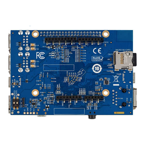
Figure 2.
STM32MP157F-DK2 bottom view
UM2637
User manual
®
®
-A7 32 bits and Cortex
-M4 32
software for the co-processor.
®
DRP HS port, USB Type-A Host
®
Low Energy 4.1, and
www.st.com
Advertisement
Table of Contents

Subscribe to Our Youtube Channel
Related Manuals for ST STM32MP157D-DK1


Summary of Contents for ST STM32MP157D-DK1
-
Page 1: Figure 1. Stm32Mp157F-Dk2 Top View
Low Energy. Extension headers allow easy ® connection of an ARDUINO board for a specific application. An ST-LINK/V2-1 is integrated on the board, as embedded in-circuit debugger and programmer for the STM32 MPU and the USB Virtual COM port bridge. Figure 1. STM32MP157F-DK2 top view Figure 2. -
Page 2: Features
GPIO expansion connector (Raspberry Pi shield capability) ® ◦ ARDUINO Uno V3 expansion connectors – On-board ST-LINK/V2-1 debugger/programmer with USB re-enumeration capability: Virtual COM port and debug port ® – STM32CubeMP1 and full mainline open-source Linux STM32 MPU OpenSTLinux Distribution (such as STM32MP1Starter) software and examples –... -
Page 3: Ordering Information
1. Additional information is available from the datasheet and reference manual of the target STM32. Table 1. List of available products Order code Board reference Target STM32 Differentiating feature STM32MP157D-DK1 • MB1272 STM32MP157DAC1 • Basic security • Secure Boot and cryptography •... -
Page 4: Development Environment
The STM32 MPU OpenSTLinux Distribution and STM32CubeMP1 base demonstration software is preloaded in ™ the microSD for easy demonstration of the device peripherals in standalone mode. The latest versions of the demonstration source code and associated documentation can be downloaded from www.st.com. UM2637 - Rev 2 page 4/47... -
Page 5: Conventions
UM2637 Conventions Conventions Table 3 provides the conventions used for the ON and OFF settings in the present document. Table 3. ON/OFF convention Convention Definition Jumper JPx ON Jumper fitted Jumper JPx OFF Jumper not fitted Jumper JPx [1-2] Jumper fitted between Pin 1 and Pin 2 Solder bridge SBx ON SBx connections closed by 0 Ω... -
Page 6: Delivery Recommendations
UM2637 Delivery recommendations Delivery recommendations Before first use, check the board for any damage that might have occurred during shipment, that all socketed components are firmly fixed in their sockets and that none are loose in the plastic bag. UM2637 - Rev 2 page 6/47... -
Page 7: Hardware Layout And Configuration
/ Mic_IN I2C1 USB Hub Host LTDC HDMI ® I2C4 USB Type- C ® RGMII Ethernet microSD™ card SDMMC ARDUINO connector ® GPIOs connectors GPIO 40-pin DDR3L GPIOs connector Feature not available on STM32MP157D-DK1 UM2637 - Rev 2 page 7/47... -
Page 8: Figure 4. Stm32Mp157X-Dkx Pcb Layout: Top Side
DDR3L (U5) User LED (LD5) User1 button (B3) User LED (LD6) STM32MP157 (U13) User2 button (B4) User LEDs (LD7, LD8) USB Hub (U7) ST-LINK STM32 (U19) HDMI ® bridge (U14) ST-LINK USB (CN11) STUSB1600 (U12) STLK LED (LD4) HDMI ®... -
Page 9: Embedded St-Link/V2-1
6.1.1 Description To debug the on-board STM32 MPU, the ST-LINK/V2-1 programming and debugging tool is integrated in the STM32MP157x-DKx Discovery kit. The embedded ST-LINK/V2-1 supports only SWD and VCP for STM32 devices. For information about the debugging and programming features of ST-LINK/V2-1, refer to the ST- LINK/V2 in-circuit debugger/programmer for STM8 and STM32 user manual (UM1075) and Overview of ST-LINK derivatives technical note (TN1235). -
Page 10: Drivers
ST-LINK/V2-1 firmware upgrade The ST-LINK/V2-1 embeds a firmware upgrade mechanism for in-situ upgrade through the USB port. As firmware may evolve during the lifetime of the ST-LINK/V2-1 product (addition of new functionalities, bug fixes, or support of new microprocessor families), visiting the www.st.com... -
Page 11: Clock Sources
The reset signal of STM32MP157x-DKx is active low. The internal PU forces the RST signal to a high level. The sources of reset are: • Reset button B2 (black button) • STPMIC1 • Embedded ST-LINK/V2-1 ® ® • ARDUINO connector CN16: pin 3, reset from the ARDUINO board •... -
Page 12: Audio
UM2637 Audio Figure 7 shows the configurations of the boot-related switch SW1. Figure 7. Boot-mode switch SW1 Forced USB boot Engineering boot Boot from SD card for flashing Audio 6.6.1 Description The audio codec is connected through an SAI interface to the STM32MP157x microcontroller. This component supports the TDM feature of the SAI port. -
Page 13: Headphone Outputs
6.6.4 Headphone outputs The STM32MP157D-DK1 and STM32MP157F-DK2 Discovery kits can drive a stereo headphone. The STM32MP157x sends the stereo audio channels to the codec via its SAI2 TDM port. The codec converts the digital audio stream to stereo analog signals. It then boosts them for direct drive of the headphone connected to the CN10 3.5 mm stereo jack receptacles on the board. -
Page 14: Usb Host
6.7.1 Description The STM32MP157D-DK1 and STM32MP157F-DK2 Discovery kits provide four USB Host ports (dual-USB sockets CN1 and CN5) through the use of the USB Hub, which has a full power management for each USB port: no I/O is needed from the STM32MP157x. -
Page 15: Usb Type-C ® Hs
® The STM32MP157D-DK1 and STM32MP157F-DK2 Discovery kits support the USB Type-C Source mode. 6.8.2 Operating voltage The STM32MP157D-DK1 and STM32MP157F-DK2 Discovery kits support 5 V USB voltage from 4.75 V to 5.25 V. 6.8.3 USB HS Source ® When a USB Device connection to the CN7 USB Type-C connector of STM32MP157D-DK1 or STM32MP157F- DK2 is detected, the Discovery kit starts behaving as a USB Host. -
Page 16: Microsd ™ Card
3.3 V voltage range: from 2.7 V to 3.6 V. All microSD card types are supported (including SDHC and SDXC), but only Default and High-Speed modes (3 V) are supported on STM32MP157D-DK1 and STM32MP157F-DK2. UHS-I modes (1.8 V) are not supported on these Discovery kits. -
Page 17: Leds
UM2637 LEDs ™ Figure 11 shows the pinout of the microSD connector CN15. ™ Figure 11. microSD card connector CN15 ™ Table 12 describes pinout of the microSD connector CN15. ™ Table 12. CN15 microSD connector pinout Pin name Signal name STM32 pin Function DAT2... -
Page 18: Operating Voltage
PD11 is connected to the blue LED LD8. Active High. 6.11 Buttons 6.11.1 Description The STM32MP157D-DK1 and STM32MP157F-DK2 Discovery kits provide four types of buttons: • Wake-up button (B1) – Allows the platform to be woken up from any low-power mode –... -
Page 19: Hdmi ® I/O Interface
UM2637 HDMI® Input signals are 24 bits digital RGB (LTDC) for the video and I2S2 for the audio. Refer to the STM32MP157x datasheet for details. The control signals are I2C1, one interruption, and a dedicated reset. ® The Consumer Electronic Control (CEC) is also available through the HDMI transmitter (transmitter bypassed). -
Page 20: Table 16. Cn9 Hdmi
UM2637 HDMI® Configuration PD12 PD12 is connected to I2C1_SCL (I2C shared). PF15 PF15 is connected to I2C1_SDA (I2C shared). PA10 PA10 is connected to HDMI_NRST ® Figure 12 shows the pinout of HDMI connector CN9. ® Figure 12. CN9 HDMI connector pinout ®... -
Page 21: Wi-Fi ® And Bluetooth ® Low Energy
UM2637 Wi‑Fi® and Bluetooth® Low Energy Pin name Signal name 5V_VIN 6.13 ® ® Wi‑Fi and Bluetooth Low Energy 6.13.1 Description ® ® The STM32MP157F-DK2 Discovery kit support Wi‑Fi 802.11b/g/n and Bluetooth Low Energy (BLE) V4.1. ® ® These functions are supported with the Wi‑Fi /BLE module. -
Page 22: Mipi Dsi Sm Lcd
PZ7 is connected to BT_DEV_WAKE LP0_32 6.14 MIPI DSI The LCD is not provided with the STM32MP157D-DK1 Discovery kit. 6.14.1 Description The 40-pin FPC connector CN4 is used to connect a TFT LCD module through the MIPI DSI interface supported by the MB1407 board. -
Page 23: Lcd Interface
UM2637 MIPI DSISM LCD 6.14.3 LCD interface Table 19 describes the I/O configuration of the LCD and CTP interfaces. Table 19. I/O configuration of the LCD and CTP interfaces Configuration DSI_D0P DSI_D0P is used as MIPI-DSI data Lane 0 positive. DSI_D0N DSI_D0N is used as MIPI-DSI data Lane 0 negative. -
Page 24: Gigabit Ethernet
Gigabit Ethernet 6.15.1 Description The STM32MP157D-DK1 and STM32MP157F-DK2 Discovery kits provide a reduced gigabit media-independent interface (RGMII). The STM32MP157x requires an external physical interface device (PHY). The Ethernet PHY on the Discovery kits is connected to the physical LAN bus using 13 signals for RGMII. It can be clocked using the 25 MHz from the STM32MP157x or from a crystal (X2). -
Page 25: Ethernet Interface
UM2637 Gigabit Ethernet 6.15.3 Ethernet interface Table 21 describes the I/O configuration of the Ethernet interface. Table 21. I/O configuration of the Ethernet interface Configuration PG0 is used as ETH_NRST active Low. PA2 is used as ETH_MDIO. PA6 is used as ETH_MDINT. PB11 is used as ETH_MDC. -
Page 26: Arduino ® Connectors
UM2637 ARDUINO® connectors Table 22. CN8 Ethernet connector pinout Pin name Function TX1+ First bidirectional pair to transmit and receive data. TX1- TX2+ Second bidirectional pair to transmit and receive data. TX2- Common connected to GND. Common connected to GND. TX3+ Third bidirectional pair to transmit and receive data. -
Page 27: Arduino ® Interface
UM2637 ARDUINO® connectors 6.16.3 ® ARDUINO interface ® Figure 16 shows the pinout of the ARDUINO connectors. ® Figure 16. ARDUINO connectors pinout ® ® ARDUINO connector ARDUINO connector (CN13) (CN14) ARDUINO ® connector ARDUINO ® connector (CN16) (CN17) ® Table 23 describes the I/O configuration of the ARDUINO interface. -
Page 28: Table 24. Pinout Of The Arduino
UM2637 ARDUINO® connectors Configuration PE1 is used as ARD_D2: IO PD14 PD14 is used as ARD_D3: TIM4_CH3 PE10 PE10 is used as ARD_D4: IO PD15 PD15 is used as ARD_D5: TIM4_CH4 PE9 is used as ARD_D6: TIM4_CH1 PD1 is used as ARD_D7: IO PG3 is used as ARD_D8: IO PH6 is used as ARD_D9: TIM12_CH1 PE11... -
Page 29: Gpio Expansion Connectors
UM2637 GPIO expansion connectors Connector Pin name Signal name STM32 pin Comment ARD_D8 ARD_D9 TIM12_CH1 ARD_D10 PE11 SPI4_NSS and TIM1_CH2 ARD_D11 PE14 SPI4_MOSI and TIM1_CH4 ARD_D12 PE13 SPI4_MISO CN13 ARD_D13 PE12 SPI4_SCK VREFP VREF+ ARD_D14 PA12 I2C5_SDA ARD_D15 PA11 I2C5_SCL 6.17 GPIO expansion connectors 6.17.1... -
Page 30: Gpio Expansion Connector Interface
UM2637 GPIO expansion connectors 6.17.2 GPIO expansion connector interface Figure 17 shows the pinout of the GPIO connectors. Figure 17. GPIO connectors CN2 pin 1 CN2 pin 2 GPIO 40-pin connector (CN2) Table 25 describes the pinout of the GPIO connectors. Table 25. -
Page 31: Vbat Connector
UM2637 VBAT connector Function STM32 pin STM32 pin Function GPIO5 / MCO2 GPIO6 / TIM5_CH2 PH11 PD13 GPIO12 / TIM4_CH2 GPIO13 /TIM3_CH2 GPIO19 / SAI2_FSA PB13 GPIO16 / USART3_CTS GPIO26 / SDMMC3_D2 GPIO20 / SAI2_SDA PF11 GPIO21 / SAI2_SDB 6.18 VBAT connector 6.18.1 Description... -
Page 32: Stm32Mp157X-Dkx Discovery Kits Information
Evaluation tools marked as “ES” or “E” are not yet qualified and therefore not ready to be used as reference design or in production. Any consequences deriving from such usage will not be at ST charge. In no event, ST will be liable for any customer usage of these engineering sample tools as reference designs or in production. -
Page 33: Board Mb1407 Revision C-01
UM2637 Board revision history 7.4.2 Board MB1407 revision C-01 The revision C-01 is the initial release of the display board MB1407. Board limitations No limitation identified for this board revision. UM2637 - Rev 2 page 33/47... -
Page 34: Stm32Mp157X-Dkx I/O Assignment
UM2637 STM32MP157x-DKx I/O assignment STM32MP157x-DKx I/O assignment Table 26. Discovery kit I/O assignment Ball Assignment BT_HOST_WAKE PH10 LTDC_R4 PH12 LTDC_R6 PH13 LTDC_G2 PH14 LTDC_G3 PH15 LTDC_G4 LTDC_G5 LTDC_G6 LTDC_G7 HDMI_I2S2_MOSI LTDC_B4 SAI2_SCKA SAI2_SDA SAI2_FSA BT_PCM_1_SDI BT_PCM_1_WS LTDC_VSYNC BT_PCM_1_CK BT_PCM_1_SDO PMIC_I2C4_SCL PG12 LTDC_B1 PMIC_I2C4_SDA... - Page 35 UM2637 STM32MP157x-DKx I/O assignment Ball Assignment ARDUINO_D8_GPIO ETH_TXD3 LTDC_B5 ETH_TXD2 GPIO5_MCO2 PG14 ETH_TXD1 HDMI_INT_GPIO PG13 ETH_TXD0 ANA0 ARDUINO_A0_ADC1_IN0 PA0_WKUP_PMIC_INT ANA1 ARDUINO_A1_ADC1_IN1 ETH_REF_CLK TypeC_Power_CC2_ADC1_IN19 TypeC_Power_CC1_ADC1_IN18 PB11 ETH_TX_EN ETH_GTX_CLK ETH_MDIO ETH_MDC ETH_CLK125 LTDC_R1 ETH_RXD2 PF15 I2C1_SDA ETH_RXD3 PF14 ARDUINO_A2_ADC2_IN6 PF13 ARDUINO_A3_ADC2_IN2 LTDC_R0 ETH_RXD1 ETH_RXD0 PF12...
- Page 36 UM2637 STM32MP157x-DKx I/O assignment Ball Assignment AB11 PG10 LTDC_B2 ARDUINO_D6_TIM1_CH1 AA11 ARDUINO_D0_UART7_RX AC10 PD11 LED_B_GPIO AB12 GPIO11_SPI5_SCK AC11 GPIO9_SPI5_MISO PF10 LTDC_DE AA13 GPIO8_SPI5_NSS PD12 I2C1_SCL AA14 GPIO10_SPI5_MOSI AC14 LTDC_CLK HDMI_CEC AC13 ARDUINO_D1_UART7_TX PE10 ARDUINO_D4_GPIO STLK_UART4_RX AA19 PD13 GPIO12_TIM4_CH2 AUDIO_RST AB19 PA12 ARDUINO_D14__GPIO3_I2C5_SDA AA18...
- Page 37 UM2637 STM32MP157x-DKx I/O assignment Ball Assignment ARDUINO_D7_GPIO WLAN_HOST_WAKE_GPIO WLAN_SDMMC2_CK BT_USART2_TX GPIO27_SDMMC3_D3 PG15 GPIO22_SDMMC3_CK LTDC_G1 GPIO24_SDMMC3_D0 GPIO23_SDMMC3_CMD GPIO25_SDMMC3_D1 BT_USART2_RTS GPIO26_SDMMC3_D2 PD10 LTDC_B3 SAI2_MCLK_A ARDUINO_D2_GPIO LTDC_R2 LTDC_R3 PE11 ARDUINO_D10_SPI4_NSS/TIM1_CH2 PE12 ARDUINO_D13_SPI4_SCK PE13 ARDUINO_D12_SPI4_MISO PH11 GPIO6_TIM5_CH2 PE14 ARDUINO_D11_SPI4_MOSI/TIM1_CH4 PE15 LTDC_R7 WLAN_REG_ON_GPIO UM2637 - Rev 2 page 37/47...
-
Page 38: Federal Communications Commission (Fcc) And Ised Canada Compliance
Federal Communications Commission (FCC) and ISED Canada Compliance Statements Federal Communications Commission (FCC) and ISED Canada Compliance Statements Identification of products: STM32MP157D-DK1 and STM32MP157F-DK2 Part 15.19 This device complies with Part 15 of the FCC Rules. Operation is subject to the following two conditions: (1) this device may not cause harmful interference, and (2) this device must accept any interference received, including interference that may cause undesired operation. - Page 39 UM2637 Additional FCC and ISED Canada Compliance Statements for STM32MP157F-DK2 Radio Frequency (RF) Exposure Compliance of Radiocommunication Apparatus To satisfy FCC and ISED Canada RF Exposure requirements for mobile devices, a separation distance of 20 cm or more should be maintained between the antenna of this device and persons during operation. To ensure compliance, operation at closer than this distance is not recommended.
-
Page 40: Ce Conformity
10.2 Simplified declaration of conformity Hereby, STMicroelectronics declares that the radio equipment types STM32MP157D-DK1 and STM32MP157F- DK2 are in compliance with Directive 2014/53/EU. The full text of the EU declaration of conformity is available from their product web page. -
Page 41: Revision History
UM2637 Revision history Table 27. Document revision history Date Revision Changes 10-Nov-2020 Initial release. Updated I/O descriptions: • PF15 configuration in Audio codec interface • Pins 11 and 12 in LCD interface • Ball Y4 assignment in STM32MP157x-DKx I/O assignment Updated Features, Development environment,... -
Page 42: Table Of Contents
ST-LINK/V2-1 firmware upgrade ........ - Page 43 UM2637 Contents 6.8.2 Operating voltage ............15 6.8.3 USB HS Source .
- Page 44 STM32MP157D-DK1 product history ........
-
Page 45: List Of Tables
CN11 ST-LINK USB Micro-B connector pinout ........ -
Page 46: List Of Figures
CN11 ST-LINK USB Micro-B connector pinout ........ - Page 47 ST’s terms and conditions of sale in place at the time of order acknowledgement. Purchasers are solely responsible for the choice, selection, and use of ST products and ST assumes no liability for application assistance or the design of Purchasers’...
Need help?
Do you have a question about the STM32MP157D-DK1 and is the answer not in the manual?
Questions and answers