
Related Manuals for THine THEVA252-SMA-V1


Summary of Contents for THine THEVA252-SMA-V1
-
Page 1: Theva252-Sma-V1 User's Guide
THEVA252-SMA-V1 User’s Guide_Rev.1.22_E THEVA252-SMA-V1 User’s Guide THCS252 Evaluation Kit Copyright© 2021, THine Electronics, Inc. THine Electronics, Inc. SC: E 1/20... -
Page 2: Table Of Contents
THEVA252-SMA-V1 User’s Guide_Rev.1.22_E Contennts THEVA252-SMA-V1 User’s Guide ......................... 1 THCS252 Evaluation Kit ..........................1 1. Introduction ............................3 1.1 Overview ............................3 1.2 Contents of evaluation kit ........................4 1.3 Quick start guide ........................... 4 2. Details about each part of the board ......................5 2.1 Power Supply ............................ -
Page 3: Introduction
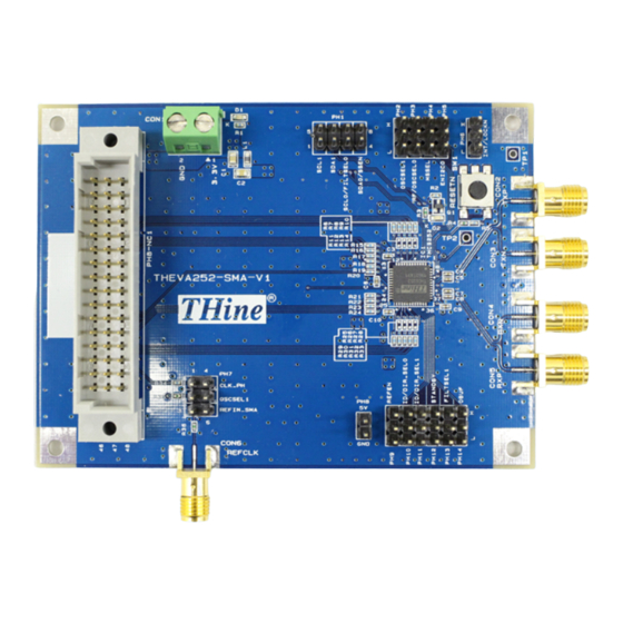
Ext. REF input 20bit I/O 20bit I/O THCS252 Master side THCS252 Slave side Figure 1 THEVA252-SMA-V1 Master Side / Slave Side top view Up Link Down Link THCS252 Master side THCS252 Slave side Figure 2 THEVA252-SMA-V1 Master Side / Slave Side bottom view Copyright©... -
Page 4: Contents Of Evaluation Kit
LSI, the sampling clock and transmission rate may vary up to +/- 20%. SMA Coaxial Cable or D1 LED for Power Connector DC1.8~3.3V D2 READY LED D2 READY LED DC1.8~3.3V D1 LED for Power Figure 3 THEVA252-SMA-V1 Quit start pin setting Copyright© 2021, THine Electronics, Inc. THine Electronics, Inc. SC: E 4/20... -
Page 5: Details About Each Part Of The Board
2.1 Power Supply For THEVA252-SMA-V1, there is a method to supply the desired voltage in the range of 1.7V to 3.6V to the CON1 power terminal block of the master side board and the slave side board. Alternatively, pins 1, 2, and 3 of 48- pin PH8 can be connected to CON1 via JP1 on the bottom of the board, power can be shared from the front and rear circuits via pins 1, 2, and 3 of PH8 is possible. -
Page 6: Full-Duplex High-Speed Signal Connector
THEVA252-SMA-V1 User’s Guide_Rev.1.22_E 2.2 Full-duplex high-speed signal connector THEVA252-SMA-V1 uses SMA connectors for high-speed signal input / output. SMA Connector SMA Connector SMAJ103-T16 Land pattern SMAJ103-T16 Mounting image Figure 6 THEVA252-SMA-V1 High Speed CML I/O connector Copyright© 2021, THine Electronics, Inc. -
Page 7: Pin Header And Connector
D15 / D4 D16 / D3 D17 / D2 D2 / D17 D1 / D18 D0 / D19 D18 / D1 D19 / D0 Figure 7 THEVA252-SMA-V1 Pin header for I/O_PH8 Copyright© 2021, THine Electronics, Inc. THine Electronics, Inc. SC: E 7/20... -
Page 8: Silk Indication Matching
THEVA252-SMA-V1 User’s Guide_Rev.1.22_E 2.3 Silk indication matching Some of the silk indication of THEVA252-SMA-V1 is inconsistent with the schematic indication and the terminal name symbol of the data sheet. The table below shows the consistency of the notation. Silk indication... -
Page 9: Schematic And Layout
THEVA252-SMA-V1 User’s Guide_Rev.1.22_E 3. Schematic and Layout 3.1 Circuit diagram. Copyright© 2021, THine Electronics, Inc. THine Electronics, Inc. SC: E 9/20... -
Page 10: Layout
THEVA252-SMA-V1 User’s Guide_Rev.1.22_E 3.2 Layout 3.2.1 L1(TOP)pattern Copyright© 2021, THine Electronics, Inc. THine Electronics, Inc. SC: E 10/20... -
Page 11: L2 Pattern
THEVA252-SMA-V1 User’s Guide_Rev.1.22_E 3.2.2 L2 pattern Copyright© 2021, THine Electronics, Inc. THine Electronics, Inc. SC: E 11/20... -
Page 12: L3 Pattern
THEVA252-SMA-V1 User’s Guide_Rev.1.22_E 3.2.3 L3 pattern Copyright© 2021, THine Electronics, Inc. THine Electronics, Inc. SC: E 12/20... -
Page 13: L4 Pattern
THEVA252-SMA-V1 User’s Guide_Rev.1.22_E 3.2.4 L4 pattern Copyright© 2021, THine Electronics, Inc. THine Electronics, Inc. SC: E 13/20... -
Page 14: Top Side Silk
THEVA252-SMA-V1 User’s Guide_Rev.1.22_E 3.2.5 TOP side silk Copyright© 2021, THine Electronics, Inc. THine Electronics, Inc. SC: E 14/20... -
Page 15: Bottom Side Silk
THEVA252-SMA-V1 User’s Guide_Rev.1.22_E 3.2.6 BOTTOM side silk Copyright© 2021, THine Electronics, Inc. THine Electronics, Inc. SC: E 15/20... -
Page 16: Top Side Implementation
THEVA252-SMA-V1 User’s Guide_Rev.1.22_E 3.2.7 TOP side implementation Copyright© 2021, THine Electronics, Inc. THine Electronics, Inc. SC: E 16/20... -
Page 17: Bottom Side Implementation
THEVA252-SMA-V1 User’s Guide_Rev.1.22_E 3.2.8 BOTTOM side implementation Copyright© 2021, THine Electronics, Inc. THine Electronics, Inc. SC: E 17/20... -
Page 18: Dimensions
THEVA252-SMA-V1 User’s Guide_Rev.1.22_E 3.2.9 Dimensions Copyright© 2021, THine Electronics, Inc. THine Electronics, Inc. SC: E 18/20... -
Page 19: Bom
R11, R12, R13, R14, R25, R26, R27, R28 Res. 1005(NC) 10kΩ(NC) 8 RK73H1ETTP1002F R54, R55 Res. 1005(NC) 0Ω(NC) 2 RK73Z1ETTP0 Top Push 1 SKHMQKE010 TP1, TP2 Test Point(NC) Through hole Copyright© 2021, THine Electronics, Inc. THine Electronics, Inc. SC: E 19/20... - Page 20 Therefore, customers are encouraged to have sufficiently redundant or error-preventive design applied to the use of the product so as not to have THine’s product cause any social or public damage. Neither replacement nor failure analysis of the product is available in any case of defects with the product and/or the product’s components.
Need help?
Do you have a question about the THEVA252-SMA-V1 and is the answer not in the manual?
Questions and answers