Table of Contents
Advertisement
Quick Links
Advertisement
Table of Contents

Related Manuals for GOWIN DK_START_GW2A-LV18PG256C8I7_V2.0


Summary of Contents for GOWIN DK_START_GW2A-LV18PG256C8I7_V2.0
- Page 1 DK_START_GW2A-LV18PG256C8I7_V2.0 RISC-V DEMO_B User Guide DBUG385-1.1E,09/10/2021...
- Page 2 Copyright © 2021 Guangdong Gowin Semiconductor Corporation. All Rights Reserved. , Gowin, and GOWINSEMI are trademarks of Guangdong Gowin Semiconductor Corporation and are registered in China, the U.S. Patent and Trademark Office, and other countries. All other words and logos identified as trademarks or service marks are the property of their respective holders.
- Page 3 Revision History Date Version Description 01/20/2021 1.0E Initial version published. 09/10/2021 1.1E The Quick Start in 2.2 A Development Board Suite removed.
-
Page 4: Table Of Contents
Contents Contents Contents ....................... i List of Figures ..................... ii List of Tables ...................... iii 1 About This Guide ..................1 1.1 Purpose ..........................1 1.2 Related Documents ......................1 1.3 Abbreviations and Terminology ................... 1 1.4 Support and Feedback ....................... 2 2 Development Board Description .............. - Page 5 3.10 LED ..........................20 3.10.1 Introduction ........................20 3.10.2 Pinout ........................... 20 3.11 Key ..........................21 3.11.1 Introduction ........................21 3.11.2 Pinout ........................... 21 3.12 Switch ..........................21 3.12.1 Introduction ........................21 3.12.2 Pinout ........................... 22 4 Gowin Software ................... 23 DBUG385-1.1E...
-
Page 6: List Of Figures
List of Figures List of Figures Figure 2-1 PCB Components ......................5 Figure 2-2 System Architecture ......................5 Figure 3-1 Connection Diagram of FPGA Download and Configuration ........... 9 Figure 3-2 Power System Distribution ....................10 Figure 3-3 Connection Diagram of Clock and Reset ................. 11 Figure 3-4 Connection Diagram of FPGA and DDR3 ................ - Page 7 List of Tables List of Tables Table 1-1 Abbreviations and Terminology ..................1 Table 3-1 FPGA Download and Pinout ....................9 Table 3-2 Clock and Reset Pinout ..................... 11 Table 3-3 DDR3 Pinout ........................12 Table 3-4 Ethernet Pinout ........................14 Table 3-5 LVDS TX Interface Pinout ....................
-
Page 8: About This Guide
An introduction to the hardware circuit functions, circuits, and pins distribution; An introduction to the use of the Gowin Software. 1.2 Related Documents The latest user guides are available on the GOWINSEMI Website. You can find the related documents at www.gowinsemi.com: 1. -
Page 9: Support And Feedback
Low-Voltage Differential Signaling SSRAM Shadow Static Random Access Memory 1.4 Support and Feedback Gowin Semiconductor provides customers with comprehensive technical support. If you have any questions, comments, or suggestions, please feel free to contact us directly using the information provided below. Website: www.gowinsemi.com... -
Page 10: Development Board Description
The development board uses the GW2A-LV18PG256 FPGA device, which is the first generation product of Gowin Arora family. The GW2A series of FPGA products offer a range of comprehensive features and rich internal resources like high-performance DSP resources, a high-speed LVDS interface, and abundant BSRAM memory resources. -
Page 11: A Development Board Suite
2.2 A Development Board Suite A development board suite includes the following items: 1. DK_START_GW2A-LV18PG256C8I7_V2.0 development board 2. 5V power adaptor (Input: 100-240V~50/60Hz 0.5A, output: DC 5V 2A) 3. USB Mini B cable Figure 2-2 A Development Board Suite ①... -
Page 12: Pcb Components
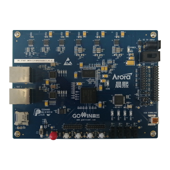
2 Development Board Description 2.3 PCB Components 2.3 PCB Components Figure 2-1 PCB Components Ethernet Interface Chip*2 1.2V 2.5V 1.0V 1.5V 3.3V Power Power Power Power Power Alternate Power DDR3 Power Socket Power Switch 20PIN Ethernet GPIO Interface*2 30PIN GPIO MODE BANK7 Level... -
Page 13: Features
2 Development Board Description 2.5 Features 2.5 Features The key features of DK_START_GW2A-LV18PG256C8I7_V2.0 are as follows: 1. The FPGA device GW2A-LV18PG256C8/I7 Max. user I/O 207 2. Download and Boot Integrates the download module; can be downloaded with the USB ... - Page 14 2 Development Board Description 2.5 Features Eight contacts, push-push type Card detection 9. Extension interface 20PIN double row pins, including 16 GPIO, one I/O Bank voltage (can be adjusted as 3.3V, 2.5V, 1.2V), one 3.3V voltage, one 5V voltage, and two ground pins.
-
Page 15: Development Board Circuit
3 Development Board Circuit 3.1 FPGA Module Development Board Circuit 3.1 FPGA Module Overview For the resources of GW2A series of FPGA Products, please refer to DS102, GW2A series of FPGA Products Data Sheet. I/O BANK Introduction For the I/O BANK, package and pinout information, please refer to UG111, GW2A series of FPGA Products Package and Pinout. -
Page 16: Pinsout
3 Development Board Circuit 3.3 Power Supply Figure 3-1 Connection Diagram of FPGA Download and Configuration P10 R10 M9 L10 3.2.2 Pinsout Table 3-1 FPGA Download and Pinout Signal Name FPGA Pin No. BANK Description JTAG_TCK 3.3V JTAG Signal JTAG_TDO 3.3V JTAG Signal JTAG_TDI... -
Page 17: Power System Distribution
3 Development Board Circuit 3.3 Power Supply 3.3.2 Power System Distribution Figure 3-2 Power System Distribution 5V 2A Power 20PIN GPIO Adaptor 30PIN GPIO NCP3170 VCCO2 & VCCO3 & Switch Power VCCO7 & VCCX 3.3V 3A (FPGA) Configure FLASH (W25Q64) Ethernet Interface Chip1 (B50610KML)... -
Page 18: Clock, Reset
3 Development Board Circuit 3.4 Clock, Reset 3.4 Clock, Reset 3.4.1 Introduction The development board offers a 50MHz oscillator, connecting to the global clock pins. It also offers a female SMA seat for users to input the external clock for multiple tests. The reset circuit adopts keys and dedicated reset chips. -
Page 19: Pinout
3 Development Board Circuit 3.5 DDR3 Figure 3-4 Connection Diagram of FPGA and DDR3 DDR3_A[13..0] DDR3_BA[2..0] DDR3_DQ[15..0] DDR3_UDM DDR3_UDQSn DDR3_UDQSp DDR3_LDM DDR3_LDQSn DDR3 SDRAM DDR3_LDQSp 2Gbit DDR3_CASn DDR3_RASn DDR3_WEn DDR3_ODT DDR3_CSn DDR3_RSTn DDR3_CK_EN DDR3_CKn DDR3_CKp 3.5.2 Pinout Table 3-3 DDR3 Pinout Signal Name FPGA Pin No. - Page 20 3 Development Board Circuit 3.5 DDR3 Signal Name FPGA Pin No. BANK Description strobe Clock Enable DDR3_CK_EN 1.5V Differential clock DDR3_CKn 1.5V Differential clock DDR3_CKp 1.5V Chip select DDR3_CSn 1.5V Data DDR3_DQ0 1.5V Data DDR3_DQ1 1.5V Data DDR3_DQ2 1.5V Data DDR3_DQ3 1.5V Data...
-
Page 21: Ethernet Interface
3 Development Board Circuit 3.6 Ethernet interface 3.6 Ethernet interface 3.6.1 Introduction The development board has two Ethernet circuits and supports gigabit mode, which can be used to test hardware environment in the LED display applications, and Ethernet data transmission. The interface connected to other devices is RJ45 with the built-in transformer. -
Page 22: Lvds Interfaces
3 Development Board Circuit 3.7 LVDS interfaces Signal Name FPGA Pin No. BANK Description PHY1_RXD2 3.3V PHY1 receive data channel 2 PHY1_RXD3 3.3V PHY1 receive data channel 3 PHY1_RX_DV 3.3V PHY1 receive data enable PHY2_GTCLK 3.3V PHY2 Transmitter Clock PHY2_TXD0 3.3V PHY2 sending data channel 0 PHY2_TXD1... -
Page 23: Pinout
3 Development Board Circuit 3.7 LVDS interfaces Figure 3-7 LVDS RX Interface LVDS_A1_P LVDS_A1_N LVDS_A1_N LVDS_A1_P LVDS_A2_P LVDS_A2_N LVDS_A2_P LVDS_A2_N LVDS_A3_P LVDS_A3_N LVDS_A3_P LVDS_A3_N LVDS_A4_P LVDS_A4_N LVDS_A4_P LVDS_A4_N LVDS_A5_P LVDS_A5_N LVDS_A5_P LVDS_A5_N 3.7.2 Pinout Table 3-5 LVDS TX Interface Pinout Pin No. -
Page 24: Sd Card
3 Development Board Circuit 3.8 SD Card Pin No. Signal Name FPGA Pin No. BANK Description 2.5V Differential Channel 4- LVDS_A4_N 2.5V Differential Channel 5+ LVDS_A5_P 2.5V Differential Channel 5- LVDS_A5_N For the V2.0 development board, J13 needs to be set as 2.5V when LVDS is used. -
Page 25: Gpio
3 Development Board Circuit 3.9 GPIO 3.9 GPIO 3.9.1 Introduction Two double row pins with the pitch of 2.54mm are reserved on the development board. The 20-pin interface connects to Bank7, and the I/O voltage can be adjusted as 3.3V, 2.5V, and 1.2V. The I/O voltage of the 30 pin can be set as 2.5V, as shown in the figure below. -
Page 26: Pinout
3 Development Board Circuit 3.9 GPIO 3.9.2 Pinout Table 3-7 20 pin Interface Pinout Pin No. Signal Name FPGA Pin No. BANK Description 3.3V / 2.5V / 1.2V General I/O H_A_IO1 3.3V / 2.5V / 1.2V General I/O H_A_IO2 3.3V / 2.5V / 1.2V General I/O H_A_IO3 3.3V / 2.5V / 1.2V General I/O H_A_IO4... -
Page 27: Led
3 Development Board Circuit 3.10 LED Pin No. Signal Name FPGA Pin No. BANK Description 2.5V General I/O H_GPIO_17 2.5V General I/O H_GPIO_18 2.5V General I/O H_GPIO_19 2.5V General I/O H_GPIO_20 2.5V General I/O H_GPIO_21 2.5V General I/O H_GPIO_22 2.5V General I/O H_GPIO_23 2.5V... -
Page 28: Key
3 Development Board Circuit 3.11 Key Note! For the V2.0 development board, the BANK0 voltage and BANK1 voltage can be set as 3.3V or 2.5V using J13. 3.11 Key 3.11.1 Introduction Four key switches are incorporated into the development board. These are used to control input during testing. -
Page 29: Pinout
3 Development Board Circuit 3.12 Switch Figure 3-13 GPIO Circuit 1.5V 3.12.2 Pinout Table 3-11 Switch Pinout Signal Name FPGA Pin No. BANK Description 1.5V Slide Switch1 1.5V Slide Switch2 1.5V Slide Switch3 1.5V Slide Switch4 DBUG385-1.1E 22(23) -
Page 30: Gowin Software
4 Gowin Software Gowin Software For the details, you can see SUG100, Gowin Software User Guide. DBUG385-1.1E 23(23)
Need help?
Do you have a question about the DK_START_GW2A-LV18PG256C8I7_V2.0 and is the answer not in the manual?
Questions and answers