
Related Manuals for Telit Wireless Solutions LE915A-P Series


Summary of Contents for Telit Wireless Solutions LE915A-P Series
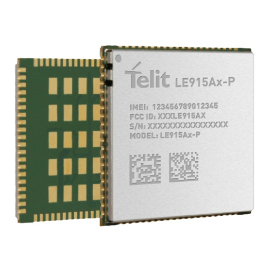
- Page 1 LE915Ax-P HW Design Guide 1VV0301680 Rev. 2 – 2021-10-04 Telit Technical Documentation...
-
Page 2: Applicability Table
Hardware Design Guide LE915Ax-P APPLICABILITY TABLE PRODUCTS LE915A6-P LE915A4-P 1VV0301680 Rev. 2 Page 2 of 51 2021-10-04 Not Subject to NDA... -
Page 3: Table Of Contents
Hardware Design Guide LE915Ax-P CONTENTS APPLICABILITY TABLE CONTENTS INTRODUCTION Scope Audience Contact Information, Support Symbol Conventions Related Documents GENERAL PRODUCT DESCRIPTION Overview Cellular Frequency Bands and CA Combinations 2.2.1. Frequency Bands 2.2.2. Carrier Aggregation (LE915A6-P only) Target Market Main Features TX Output Power RX Sensitivity Mechanical Specifications... - Page 4 Hardware Design Guide LE915Ax-P 4.4.1.1. +5V Source Power Supply Design Guidelines 4.4.2. Thermal Design Guidelines 4.4.3. Power Supply PCB Layout Guidelines INTERFACE DETAILS Power On.Off and Reset Control 5.1.1. Power On Sequence 5.1.2. Power Off Sequence Communication Ports 5.2.1. USB 2.0 Interface 5.2.2.
- Page 5 Hardware Design Guide LE915Ax-P Packaging Detail Moisture Sensitivity REGULATORY APPROVAL PRODUCT AND SAFETY INFORMATION Copyrights and Other Notices 11.1.1. Copyrights 11.1.2. Computer Software Copyrights Usage and Disclosure Restrictions 11.2.1. License Agreements 11.2.2. Copyrighted Materials 11.2.3. High Risk Materials 11.2.4. Trademarks 11.2.5.
-
Page 6: Introduction
Hardware Design Guide LE915Ax-P 1. INTRODUCTION Scope This document introduces the Telit LE915Ax-P family and presents possible and recommended hardware solutions for the development of a product based on the LE915Ax-P modules. In this document all the basic functions of the module will be considered; for each of them a suitable hardware solution will be suggested and eventually the wrong solutions and common errors to be avoided will be evidenced. -
Page 7: Symbol Conventions
Hardware Design Guide LE915Ax-P TS-ONEEDGE@telit.com • Alternatively, use: https://www.telit.com/contact-us/ Product information and technical documents are accessible 24/7 on our web site: https://www.telit.com Symbol Conventions Danger: This information MUST be followed or catastrophic equipment failure or personal injury may occur. Warning: Alerts the user on important steps about the module integration. -
Page 8: General Product Description
Hardware Design Guide LE915Ax-P 2. GENERAL PRODUCT DESCRIPTION Overview LE915Ax-P family consists of an LTE CAT-6 and CAT-4 modules and is specifically designed to enable cellular data connectivity on CBRS networks operating on TDD LTE band 48 in US. It can also operate on other networks operating on LTE bands 42 and 43. This document provides technical information about LE915Ax-P LCC modules. -
Page 9: Main Features
Hardware Design Guide LE915Ax-P Main Features Main features of the LE915Ax-P are listed below. Feature Description LCC (32 x 29 x2.4mm), Physical 134 pads carrying useful signals Power supply Nominal 3.8V single power supply Operating voltage -30 ~ +60 °C ambient recommended USB 2.0, 1 High Speed UART with HW flow control and 2 Low Speed UARTs w/o flow Serial interface... -
Page 10: Mechanical Specifications
Hardware Design Guide LE915Ax-P Mechanical Specifications 2.7.1. Dimensions and LCC Pads Layout The overall dimensions of LE915Ax-P family are: • Length: 32 mm • Width: 29 mm • Thickness: 2.4 mm 2.7.2. Weight The nominal weight of the LE915Ax-P family is 5.1 grams. Temperature Range Tempeurature Range Note... -
Page 11: Pins Allocation
Hardware Design Guide LE915Ax-P 3. PINS ALLOCATION Pin-out Signal Function Type Comment USB HS 2.0 COMMUNICATION PORT USB_D+ USB differential Data (+) 3.3V USB_D- USB differential Data (-) 3.3V USB_EXT_VBUS_VLD USB port detection 1.8V Asynchronous Serial Ports UART2_SIN Serial data input from DTE 1.8V UART2 UART2_SOUT... - Page 12 Hardware Design Guide LE915Ax-P Signal Function Type Comment Miscellaneous Functions MODULE_PWR_EN Module power ON/OFF control 1.8V RESET_N Reset control 1.8V Active low NETWORK_LED Downlink status indication LED HWID1 Reserved 1.8V HWID2 Reserved 1.8V FFF_FFH Reserved 1.8V J-TAG TRST_N Reserved, JTAG for debugging Reserved, JTAG for debugging Reserved, JTAG for debugging Reserved, JTAG for debugging...
- Page 13 Hardware Design Guide LE915Ax-P Signal Function Type Comment Ground Power Ground Power Ground Power Ground Power Ground Power Ground Power Ground Power Ground Power Ground Power Ground Power Ground Power Ground Power Ground Power Ground Power Ground Power Ground Power Ground Power Ground...
- Page 14 Hardware Design Guide LE915Ax-P Signal Function Type Comment RESERVED RESERVED RESERVED RESERVED RESERVED RESERVED RESERVED RESERVED RESERVED RESERVED RESERVED RESERVED RESERVED RESERVED RESERVED RESERVED RESERVED RESERVED RESERVED RESERVED RESERVED RESERVED RESERVED RESERVED RESERVED RESERVED RESERVED RESERVED RESERVED RESERVED RESERVED RESERVED RESERVED RESERVED RESERVED...
- Page 15 Hardware Design Guide LE915Ax-P Signal Function Type Comment RESERVED RESERVED RESERVED RESERVED RESERVED RESERVED RESERVED RESERVED RESERVED RESERVED RESERVED RESERVED RESERVED RESERVED RESERVED RESERVED RESERVED RESERVED RESERVED RESERVED RESERVED RESERVED RESERVED RESERVED RESERVED RESERVED RESERVED RESERVED RESERVED RESERVED RESERVED RESERVED RESERVED RESERVED RESERVED...
-
Page 16: Power Supply
Hardware Design Guide LE915Ax-P 4. POWER SUPPLY The power supply circuitry and the board layout are a very important part in the full product design and they strongly reflect on the product overall performances, so the requirements and the guidelines that will follow should be read carefully for a proper design. -
Page 17: Power Output
Hardware Design Guide LE915Ax-P 1.8V Power Output The pad, 1V8_D, is a reference voltage output for IOs. It can be used to provide 1.8V power to small devices up to 50mA max. Signal Typical (V) Min (V) Max (V) 1V8_D 1.71 1.89 Table... -
Page 18: Thermal Design Guidelines
Hardware Design Guide LE915Ax-P Figure 1: An Example of Linear Regulator with 5V Input 4.4.2. Thermal Design Guidelines Thermal dispersion needs to be carefully considered in entire customer device design. The power supply heat sink must be dimensioned according to the following guidelines: •... - Page 19 Hardware Design Guide LE915Ax-P • The Bypass low ESR capacitor must be placed close to the power input pads or, in the case the power supply is of a switching type it can be placed close to the inductor to cut the ripple, provided the PCB trace from the capacitor to Telit module is wide enough to ensure a voltage dropless connection.
- Page 20 Hardware Design Guide LE915Ax-P Figure 2: Recommended Circuit of EMI filter 1VV0301680 Rev. 2 Page 20 of 51 2021-10-04 Not Subject to NDA...
-
Page 21: Interface Details
Hardware Design Guide LE915Ax-P 5. INTERFACE DETAILS Power On.Off and Reset Control The Telit module can be turned on/off by means of the MODULE_PWR_EN port. The module enters Power on Reset mode when the RESET_N is set logical LOW. While the device power-on sequence is still in progress, the two conditions below must be avoided: •... -
Page 22: Communication Ports
Hardware Design Guide LE915Ax-P Figure 3: Power off sequence Communication Ports 5.2.1. USB 2.0 Interface The USB controller of LE915Ax-P is compliant with USB 2.0 specification and the data rate up to 480Mbps. PCB routes must be designed so that USB lines are 90 Ohm differential. -
Page 23: Uart Interfaces
Hardware Design Guide LE915Ax-P Figure 4: example of USB interface circuit Note: On the application board. It is highly recommended to insert an optional connector or test points that can be switched for direct connection of the external PC for a later SW upgrade or debugging. 5.2.2. - Page 24 Hardware Design Guide LE915Ax-P • microcontroller UART @ 5V or other voltages different from 1.8V Depending on the type of serial port on the OEM hardware, a level translator circuit may be required to operate the system. On the LE915Ax-P family, the ports are CMOS 1.8V. Note: When UART signals are used as the communication port between the host and the modem and flow control is not used, UART2_CTS line must set to logical LOW.
-
Page 25: Rs232 Level Translation
Hardware Design Guide LE915Ax-P Figure 6: Two types of typical UART interface without HW flow control 5.2.2.1. RS232 Level Translation Depending on the serial port type on the application side, a level translator circuit may be required. The nominal voltage level of the UART interface is 1.8V. Following figure shows a typical level translator circuit for interfacing the external device with the UART ports. -
Page 26: General Purpose I/O
Hardware Design Guide LE915Ax-P Figure 7: Typical level translator circuit Warning: The digital input lines, operating at 1.8V CMOS levels, have an absolute maximum input voltage of 3.6V. The IC outputs of the level transducer on the side of the module (that is LE915Ax-P inputs) will damage the inputs of the module if the level translator is also powered with nominal power of 3.8V. -
Page 27: Led Indication
Hardware Design Guide LE915Ax-P Signal Function description GPIO_5 1.8V, 8mA Table 15: Available GPIO LED Indication The downlink status indicator output is provided to indicate. Refer to the typical non- inverting type LED driver circuit below. Signal Function description NETWORK_LED Active LOW indicates when packets go through network interface. -
Page 28: Reserved Pins
Hardware Design Guide LE915Ax-P Note: If the application requires SIM card insertion or removal support, the SIM card handler must include a removal/insertion pad detector to allow the module firmware to process the event immediately. The default SW configuration is to support SIM_DETECT. If the SIM holder doesn’t have a SIM detect switch, it is required to keep HIGH the SIM_DETECT port to avoid floating and to ensure that the SIM is always detected as present. -
Page 29: Rf Section
Hardware Design Guide LE915Ax-P 6. RF SECTION Antenna Requirements The antenna connection and board layout design are the most important aspect in the full product design as they strongly affect the general performance of the product, so read carefully and follow the requirements and the guidelines for a proper design. Signal Function description ANT_MAIN... -
Page 30: Pcb Guidelines In Case Of Fcc Certification
Hardware Design Guide LE915Ax-P • keep the line on the PCB as short as possible, since the antenna line loss shall be less than about 0,3 dB; • the geometry of the line must have uniform characteristics, constant cross section, avoid meanders and abrupt curves; •... -
Page 31: Transmission Line Design
Hardware Design Guide LE915Ax-P 6.1.2.1. Transmission Line Design When designing an interface board, the placement of components was chosen properly, in order to keep the length of the line as short as possible, thus leading to the least possible power loss. A Grounded Coplanar Waveguide (G-CPW) line has been chosen, this kind of transmission line ensures good impedance control and can be implemented in an external PCB layer as needed in this case. - Page 32 Hardware Design Guide LE915Ax-P Return Loss plot of line under test is shown below: Figure 11: Return Loss plot of line under test The input impedance of the line (in Smith Chart format, once the line has been terminated to 50 Ω load) is shown in the following figure: Figure 12: Line input impedance Insertion Loss of G-CPW line plus SMA connector is shown below: 1VV0301680 Rev.
-
Page 33: Antenna Installation Guidelines
Hardware Design Guide LE915Ax-P Figure 13: Insertion Loss of G-CPW line plus SMA connector 6.1.2.3. Antenna Installation Guidelines • Install the antenna in a place covered by the LTE signal with CAT-M1 support. • The Antenna must not be installed inside metal cases. •... -
Page 34: Mechanical Design
Hardware Design Guide LE915Ax-P 7. MECHANICAL DESIGN Drawing Figure 14: Mechanical Design Drawing 1VV0301680 Rev. 2 Page 34 of 51 2021-10-04 Not Subject to NDA... -
Page 35: Application Pcb Design
Hardware Design Guide LE915Ax-P 8. APPLICATION PCB DESIGN The XX123Z4 modules have been designed in order to be compliant with a standard lead- free SMT process. PCB Pad Design In PCB design, the solder pads can be defined either as Solder Mask Defined (SMD) or Non-Solder Mask Defined (NSMD). - Page 36 Hardware Design Guide LE915Ax-P Figure 16: Recommended Solder Reflow Profile Profile Feature Pb-Free Assembly Free Preheat – Temperature Min (Tsmin) 150°C – Temperature Max (Tsmax) 200°C – Time (min to max) (ts) 105+/-15 seconds Dwell Time (Liquidous Time) – Temperature Min (Tsmin) 220°C –...
-
Page 37: Inspection
Hardware Design Guide LE915Ax-P Inspection An inspection of the solder joint between the solder pads of the Telit module and the application PCB should be performed. The best visual inspection tool for inspection of the Telit module solder joints on the PCB is a transmission X-ray, which can identify defects such as solder bridging, shorts, opens, and large voids (Note: small voids in large solder joints are not detrimental to the reliability of the solder joint). -
Page 38: Packaging
Hardware Design Guide LE915Ax-P 9. PACKAGING Reel The LE915Ax-P is delivered in Tape-and-Reel. One reel can hold up to 500 pieces. Each reel is included in a box, and a carton can contain five boxes, hence up to 2500 pieces. Figure 17: Module Positioning into the Carrier Carrier Tape Detail Figure 18: Carrier Tape Detail... -
Page 39: Packaging Detail
Hardware Design Guide LE915Ax-P Packaging Detail Figure 19: Packaging Detail Moisture Sensitivity The LE915Ax-P family is a Moisture Sensitive Device level 3, in accordance with the IPC/JEDEC J-STD-020 standard, takes care all related requirements for the use of this kind of components. Moreover, the customer must take care of the following conditions: 1VV0301680 Rev. - Page 40 Hardware Design Guide LE915Ax-P a) Calculated shelf life in sealed bag: 12 months at <40°C and <90% relative humidity (RH). b) Environmental condition during the production: 30°C / 60% RH according to IPC/JEDEC J-STD-033A paragraph 5. c) The maximum time between the opening of the sealed bag and the reflow process must be 168 hours if condition b) “IPC/JEDEC J-STD-033D paragraph 5.2”...
-
Page 41: Regulatory Approval
Hardware Design Guide LE915Ax-P 10. REGULATORY APPROVAL This following statement applies to all products based on Telit LE915Ax-P supporting Band 48 that would be deployed in CBRS network in USA. This device complies with Part 15 of the FCC Rules. Operation is subject to the following two conditions: (1) This device may not cause harmful interference, and (2) this device must accept any interference received, including interference that may cause undesired operation. - Page 42 Hardware Design Guide LE915Ax-P Radiation Exposure Statement: This equipment complies with FCC radiation exposure limits set forth for an uncontrolled environment. This equipment should be installed and operated with a minimum distance 20cm between the radiator & your body. This module is intended for OEM integrators only. Per FCC KDB 996369 D03 OEM Manual v01 guidance, the following conditions must be strictly followed when using this certified module: KDB 996369 D03 OEM Manual v01 rule sections:...
- Page 43 Hardware Design Guide LE915Ax-P • LTE band 48 : Max. 0.5 dBi, assuming 0.5 dB attenuation loss between LCC module pad and antenna SMA connector. The dipole antenna must be installed such that 20cm can be maintained between the antenna and users to comply with the FCC maximum EIRP limits and RF Exposure rules. 2.8 Label and compliance information The final end product must be labeled in a visible area with the following: "Contains FCC ID: RI7LE915A6"...
- Page 44 Hardware Design Guide LE915Ax-P OEM/Host manufacturer responsibilities OEM/Host manufacturers are ultimately responsible for the of Host and Module compliance. The final product must be reassessed against all FCC essential requirements such as FCC Part 15 Subpart B before it can be placed on the US market. This includes reassessing the transmitter module for compliance with the Radio and EMF essential requirements of the FCC rules.
-
Page 45: Product And Safety Information
Hardware Design Guide LE915Ax-P 11. PRODUCT AND SAFETY INFORMATION Copyrights and Other Notices SPECIFICATIONS ARE SUBJECT TO CHANGE WITHOUT NOTICE Although reasonable efforts have been made to ensure the accuracy of this document, Telit assumes no liability resulting from any inaccuracies or omissions in this document, or from the use of the information contained herein. -
Page 46: Usage And Disclosure Restrictions
Hardware Design Guide LE915Ax-P computer programs, including – but not limited to - the exclusive right to copy or reproduce in any form the copyrighted products. Accordingly, any copyrighted computer programs contained in Telit’s products described in this instruction manual shall not be copied (reverse engineered) or reproduced in any manner without the express written permission of the copyright owner, being Telit or the Third Party software supplier. -
Page 47: Trademarks
Hardware Design Guide LE915Ax-P 11.2.4. Trademarks TELIT and the Stylized T-Logo are registered in the Trademark Office. All other product or service names are property of their respective owners. 11.2.5. Third Party Rights The software may include Third Party’s software Rights. In this case the user agrees to comply with all terms and conditions imposed in respect of such separate software rights. -
Page 48: Safety Recommendations
Hardware Design Guide LE915Ax-P Safety Recommendations Make sure the use of this product is allowed in your country and in the environment required. The use of this product may be dangerous and has to be avoided in areas where: • it can interfere with other electronic devices, particularly in environments such as hospitals, airports, aircrafts, etc. -
Page 49: Glossary
Hardware Design Guide LE915Ax-P 12. GLOSSARY Carrier Aggregation CBRS Citizens Band Radio Service Down Link EIRP Effective Isotopically Radiated Power Electrical Over Shock Electrostatic Discharge Equivalent Series Resistance E-UTRA Evolved Universal Terrestrial Radio Access Leadless Chip Carrier Long Term Evolution Machine to machine Point of Sales Printed Circuit Board... -
Page 50: Document History
Hardware Design Guide LE915Ax-P 13. DOCUMENT HISTORY Revision Date Changes 2021-10-04 Doc format changed 2021-09-24 Temperature range updated UART diagram updated Added GPIOs related description Max data rate described in the USB and UART interfaces Description changes on LED indication Updated the decription of power on sequence and timing Updates on related documents in chapter 1.5 Updates on current consumption...
Need help?
Do you have a question about the LE915A-P Series and is the answer not in the manual?
Questions and answers