Table of Contents
Advertisement
Quick Links
Evaluates: MAX77831
General Description
The MAX77831 evaluation kit (EV kit) provides a proven
design to evaluate the MAX77831, a 7A switching current,
high-efficiency, high-performance buck-boost regulator
that only operates in forced-PWM (FPWM) mode. The IC
is capable of 2.5V to 16V input and dynamically adjust-
able output between 4.5V to 15V when using internal
feedback resistors, or between 3V to 15V when using
external feedback resistors. The EV kit is factory-config-
ured as internal feedback with the default startup output
voltage at 5V. Other startup voltage can be achieved
with external feedback resistors. Output voltage can be
adjusted dynamically through the I
The I/O pins are available to support the I
face, Enable function, and Interrupt/Power-OK indicator.
2
The I
C slave address, switching current limit, and feed-
back configuration can be adjusted by changing the R
resistor value (R9). The MAXUSB_INTERFACE# allows
®
the use of Windows
-based software with a friendly
graphical user interface (GUI) as well as a detailed regis-
ter-based interface to exercise all the features of the IC.
The IC installed on the EV kit is the MAX77831BEWB+T.
MAX77831 EV Kit Specifications
SPECIFICATION
Input Voltage
Output Voltage
Default Output Voltage
Switching Current Limit
Peak Efficiency
Windows is a registered trademark of Microsoft Corp.
©
2021 Analog Devices, Inc. All rights reserved. Trademarks and registered trademarks are the property of their respective owners.
One Analog Way, Wilmington, MA 01887 U.S.A.
Click
2
C serial interface.
2
C serial inter-
SEL
TEST CONDITION
Internal Feedback
External Feedback
Internal Feedback
V
= 4V, V
= 5V, 700mA Load
IN
OUT
|
Tel: 781.329.4700
here
to ask an associate for production status of specific part numbers.
MAX77831 Evaluation Kit
Benefits and Features
● Proven PCB Reference Design and Layout Benefit
● Fully Assembled and Tested
● Sense Points for High-Accuracy Measurements
● Accessible Test Point Pins for EN, POKB/INTB, V
2
and the I
C Serial Interface SCL, SDA
● MAXUSB_INTERFACE# Allows Easy Communication
with a Windows PC
● GUI Software that Drives the I
Optional Software Control
● Startup Output Voltage Adjustable Through External
Feedback Resistors
● Output Voltage Dynamically Adjustable Through the
2
I
C Serial Interface
2
● I
C Slave Address, Switching Current Limit, and
Feedback Configuration Adjustable Using R
Ordering Information
|
© 2021 Analog Devices, Inc. All rights reserved.
2
C Serial Interface for
appears at end of data sheet.
MIN
TYP
MAX
2.5
16
4.5
15
3
15
5
7
97.0
319-100600; Rev 1; 9/21
,
IO
(R9)
SEL
UNIT
V
V
V
V
A
%
Advertisement
Table of Contents

Related Manuals for Analog Devices MAX77831


Summary of Contents for Analog Devices MAX77831
- Page 1 Windows is a registered trademark of Microsoft Corp. 319-100600; Rev 1; 9/21 © 2021 Analog Devices, Inc. All rights reserved. Trademarks and registered trademarks are the property of their respective owners. One Analog Way, Wilmington, MA 01887 U.S.A. Tel: 781.329.4700...
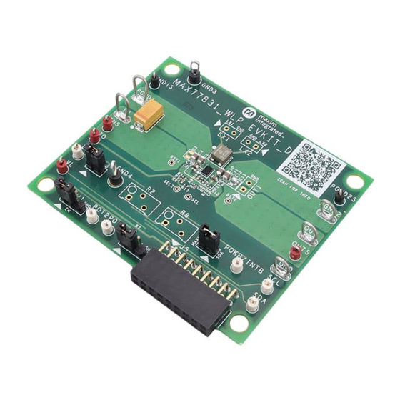
- Page 2 15kΩ 10V 0402 0402 POK/ POKB/I NTB OPTIONAL INTERRUPT C INTERFACE AGND PGND *CHOOSE R VALUE SEL * BASED ON TAB LE 2 Figure 1. Application Circuit for MAX77831 Figure 2. MAX77831 EV Kit Photo Analog Devices │ 2 www.analog.com...
-
Page 3: Quick Start
(R9) = 0Ω, R (R10) to measure input voltage. = 0Ω, and R (R11) = OPEN, the MAX77831 EV kit is 3) Connect a DVM to the OUTS and PGND2S sense configured with the following settings: pins to measure output voltage. - Page 4 EV kit. Output voltage step size can be calculated with the fol- Configuration Resistor lowing equation: The MAX77831 includes an SEL pin to set the I C slave 4.9mV address, switching current limit, and feedback configura- ×...
- Page 5 • Warning: Setting this incorrectly to 3.3V could EV kit GUI software allows users to easily change the potentially damage the MAX77831 IC. MAX77831’s register settings with a Windows PC. Before connecting the MAXUSB_INTERFACE# to the EV kit’s The MAXUSB_INTERFACE# also includes an on-board...
- Page 6 MAX77831’s and line regulation measurements, use these sense pins I/O logic voltage level. Refer to the MAX77831 IC data to measure input and output voltages. sheet for the appropriate I/O logic voltage level.
-
Page 7: Installation
The Device Synchronization menu opens (Figure Installation once the MAX77831 IC responds (voltages on IN pin and V pin must be valid on the MAX77831 IC for it Visit the product webpage at https://www.maximinte- to respond). The I C address shown is the MAX77831 grated.com/products/MAX77831WEVKIT... - Page 8 (Figure 9) configures the reflection of the bits in INT_SRC window to apply all settings to the MAX77831’s registers. to the POKB/INTB pin. If a bit is masked, its status in Alternatively, click Read on each setting section to obtain...
- Page 9 MAX77831 Evaluation Kit Evaluates: MAX77831 Figure 7. Configuration Tab - Chip Identification Section Figure 8. Configuration Tab - POK Status and Fault Interrupt Source Section Figure 9. Configuration Tab - POK Status and Fault Interrupt Masks Section Analog Devices │ 9...
- Page 10 (using the internal refer- corresponding to the EV kit configuration. For external ence voltage DVS slew rate). Refer to the MAX77831 IC feedback configuration, enter the chosen feedback resis- data sheet for more information on each available setting.
-
Page 11: Layout Guidelines
HDI PCB lay- to further reduce trace impedance. Furthermore, do outs for the MAX77831 WLP package. Use the provided not make LX traces take up an excessive amount of layout files for guidance when designing with the IC. The area. - Page 12 Do not create PGND islands, as PGND Refer to the Output Capacitor Selection section in the islands risk interrupting the hot loops. Connect AGND MAX77831 IC datasheet and Tutorial 5527 for more and AGND island to the low-impedance ground plane information.
-
Page 13: Ordering Information
MAX77831 Evaluation Kit Evaluates: MAX77831 **LAYOUT BASED ON LEGEND 3.8A I CONFIGURATION 1008 (2520) PGND PGND 1008 (2520) 0603 0402 BST1 BST2 NON-HDI VIA BST1 BST2 8mil HOLE, 16mil PAD 0603 0603 6mil HOLE, 12mil PAD HDI µVIA *USING INTERNAL... - Page 14 MAX77831 Evaluation Kit Evaluates: MAX77831 MAX77831 EV Kit Bill of Materials REF_DES MFG PART # MANUFACTURER VALUE DESCRIPTION CAPACITOR; SMT (7343-43); TANTALUM CHIP; T491X107K025A KEMET 100µF 100µF; 25V; TOL = 10% JMK105B7474KVHF TAIYO YUDEN 0.47µF CAP; SMT (0402); 0.47µF; 10%; 6.3V; X7R; CERAMIC CHIP CAPACITOR;...
- Page 15 MAX77831 Evaluation Kit Evaluates: MAX77831 MAX77831 EV Kit Schematic Diagram Analog Devices │ 15 www.analog.com...
- Page 16 MAX77831 Evaluation Kit Evaluates: MAX77831 MAX77831 EV Kit Schematic Diagram MECHANICAL STAND OFF 9032 9032 02-SOM35016H-00 02-SOM35016H-00 SPACER SPACER 9032 9032 02-SOM35016H-00 02-SOM35016H-00 SPACER SPACER Analog Devices │ 16 www.analog.com...
- Page 17 MAX77831 Evaluation Kit Evaluates: MAX77831 MAX77831 EV Kit PCB Layout Diagrams 1.0” 1.0” MAX77831 EV Kit PCB Layout — Top Silkscreen MAX77831 EV Kit PCB Layout — Internal 2 1.0” 1.0” MAX77831 EV Kit PCB Layout — Top View MAX77831 EV Kit PCB Layout — Internal 3 Analog Devices │...
- Page 18 Evaluates: MAX77831 MAX77831 EV Kit PCB Layout Diagrams (continued) 1.0” 1.0” MAX77831 EV Kit PCB Layout — Internal 4 MAX77831 EV Kit PCB Layout — Internal 5 1.0” MAX77831 EV Kit PCB Layout — Bottom View Analog Devices │ 18...
-
Page 19: Revision History
Information furnished by Analog Devices is believed to be accurate and reliable. However, no responsibility is assumed by Analog Devices for its use, nor for any infringements of patents or other rights of third parties that may result from its use.Specifications subject to change without notice. No license is granted by implicationor otherwise under any patent or patent rights of Analog Devices.
Need help?
Do you have a question about the MAX77831 and is the answer not in the manual?
Questions and answers