Table of Contents
Advertisement
Quick Links
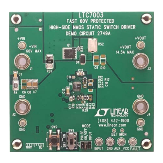
DESCRIPTION
Demonstration circuit 2749A is a 60V protected, high
side switch featuring the
designed to switch a 14.5A output load from input volt-
ages from 6V to 60V. The wide input range and low shut-
down current (1µA typical) make it suitable for automo-
tive, industrial, medical instrument and telecom applica-
tions. This board offers a low 45ns (typical) propagation
delay, fast switching times (<10ns) and 100% duty cycle
operation.
The LTC7003 is a fast protected high side N-channel
MOSFET driver. An internal charge pump fully enhances
an external N-channel MOSFET switch, allowing it to
remain on indefinitely. Its powerful gate driver can drive
large gate capacitance MOSFETs with very short transition
times, ideal for both high frequency switching and static
switch applications. The LTC7003 operates over a 3.5V to
60V input supply range. When an external current sense
resistor and internal comparator sense that the switch
current has exceeded a preset level, a fault flag is asserted
and the switch is turned off after a period of time set
by an external timing capacitor. After a cooldown period,
the LTC7003 can be configured to automatically retry or
remain off until the input is recycled.
PERFORMANCE SUMMARY
SYMBOL
PARAMETER
V
Input Voltage
IN
I
Output Current
OUT
Insertion Drop
V
Start-Up Voltage
IN
V
V
Undervoltage Lockout
CCUV
CC
Overcurrent to V
Low
OUT
Input to Output Propagation Delay
Output Rise Time
LTC
7003. The demo board is
®
Specifications are at T
CONDITIONS
V
– V
, 14.5A Load, Input to Output Terminals
IN
OUT
V
= 4V
INP
100kΩ Load
V
Rising
CC
V
Falling
CC
Hysteresis
Turn-On into a 25A Resistive Load
V
= 60V, 50Ω Load, INP = 2.2V to V
IN
V
= 60V, 50Ω Load, 10% to 90%
IN
DEMO MANUAL DC2749A
Fast 60V Protected High Side
NMOS Static Switch Driver
The demo board includes input capacitors and output
diode to accommodate input and output supply induc-
tance when switching loads. The switch can be controlled
directly with external signal or using the on-board on/off
switch. A single-shot pulse generator is included for evalu-
ating switching times while limiting output power. Optional
auxiliary V
input accommodates gate power associated
CC
with high frequency switching. Positions for RC delay net-
work to control inrush current are also included.
The LTC7003 data sheet gives a complete description of
the part, operation and application information. The data
sheet must be read in conjunction with this demo manual
for demo circuit 2749A. Proper board layout is essential
for maximum thermal and electrical performance. See the
data sheet sections for details. The LTC7003 is available
in 16-lead MSOP package and three operating junction
temperature grades extended and industrial from –40°C
to 125°C, high temp automotive from –40°C to 150°C and
a military grade from –55°C to 150°C.
Design files for this circuit board are available at
http://www.linear.com/demo/DC2749A
All registered trademarks and trademarks are the property of their respective owners.
= 25°C
A
= 6V
OUT
LTC7003
MIN
TYP
MAX
UNITS
60
14.5
81
7.0
6.0
5.1
4.6
0.5
19
45
9
dc2749af
V
A
mV
V
V
V
V
V
µs
ns
ns
1
Advertisement
Table of Contents

Related Manuals for Linear Analog Devices DC2749A


Summary of Contents for Linear Analog Devices DC2749A
- Page 1 Design files for this circuit board are available at by an external timing capacitor. After a cooldown period, http://www.linear.com/demo/DC2749A the LTC7003 can be configured to automatically retry or All registered trademarks and trademarks are the property of their respective owners.
- Page 2 DEMO MANUAL DC2749A QUICK START PROCEDURE Refer to Figure 1 for proper measurement equipment 5. Place SW1 to ON position. setup and follow the procedure below: 6. Check for the proper output voltage using a voltmeter. NOTE: When measuring the output voltage during switch- Output voltage should be close to input voltage.
- Page 3 DEMO MANUAL DC2749A QUICK START PROCEDURE – Figure 2. Measuring Output Voltage During Switching across C9. Note that C9 May Not Be Installed TYPICAL PERFORMANCE CHARACTERISTICS 20V/DIV 2V/DIV Figure 3. Rise Time into 50Ω Load (V = 60V, V 2V/DIV, V 20V/DIV, 20ns/DIV) Figure 4.
- Page 4 RES, 0Ω, 1/10W, 1%, 0603 VISHAY CRCW06030000Z0EA RES, 1MEG, 1/10W, 1%, 0805 VISHAY CRCW08051M00FKEA IC, LTC7003EMSE, MSE-16 LINEAR TECH, LTC7003EMSE#PBF Additional Demo Board Circuit Components CAP , 10nF, X7R, 100V, 10%, 1206 AVX, 12061C103KAZ2A CAP , 100µF, ELECT, 63V, 20%, TH C-10X12.5...
- Page 5 VISHAY CRCW0603182KFKEA SWITCH, SUB MINITURE SLIDE C&K COMPONENTS, JS202011CQN SWITCH, MICRO MINATURE PUSHBUTTON TE CONNECTIVITY, FSM4JSMA IC, LTC6993CS6-3, TSOT23-6 LINEAR TECH, LTC6993CS6-3#PBF Hardware: For Demo Board Only E1 TO E8 TESTPOINT, TURRET 0.094" MILL MAX 2501-2-00-80-00-00-07-0 CONN., HEADER, 2X3, 2mm...
- Page 6 DEMO MANUAL DC2749A SCHEMATIC DIAGRAM dc2749af...
- Page 7 DEMO MANUAL DC2749A SCHEMATIC DIAGRAM dc2749af Information furnished by Analog Devices is believed to be accurate and reliable. However, no responsibility is assumed by Analog Devices for its use, nor for any infringements of patents or other rights of third parties that may result from its use. Specifications subject to change without notice.
- Page 8 DEMO MANUAL DC2749A ESD Caution ESD (electrostatic discharge) sensitive device. Charged devices and circuit boards can discharge without detection. Although this product features patented or proprietary protection circuitry, damage may occur on devices subjected to high energy ESD. Therefore, proper ESD precautions should be taken to avoid performance degradation or loss of functionality. Legal Terms and Conditions By using the evaluation board discussed herein (together with any tools, components documentation or support materials, the “Evaluation Board”), you are agreeing to be bound by the terms and conditions set forth below (“Agreement”) unless you have purchased the Evaluation Board, in which case the Analog Devices Standard Terms and Conditions of Sale shall govern.
Need help?
Do you have a question about the Analog Devices DC2749A and is the answer not in the manual?
Questions and answers