Advertisement
This user's guide describes the characteristics, operation, and use of the 2N7001TEVM Evaluation Module
(EVM). The complete printed-circuit board (PCB) layout, schematic diagram, and bill of materials are
included in this document.
...................................................................................................................
1
2
Board Layout
3
Schematic and Bill of Materials
1
2
J2 Header Simplified Diagram
3
4
1
Trademarks
All trademarks are the property of their respective owners.
SCEU013 - May 2018
Submit Documentation Feedback
................................................................................................................
............................................................................................
........................................................................................................
.............................................................................................
.......................................................................................................
...................................................................................................
...............................................................................................................
Copyright © 2018, Texas Instruments Incorporated
2N7001T Evaluation Module
Contents
List of Figures
List of Tables
User's Guide
SCEU013 - May 2018
2N7001T Evaluation Module
2
4
4
2
3
4
4
5
1
Advertisement
Table of Contents

Subscribe to Our Youtube Channel
Related Manuals for Texas Instruments 2N7001TEVM


Summary of Contents for Texas Instruments 2N7001TEVM
-
Page 1: Table Of Contents
User's Guide SCEU013 – May 2018 2N7001T Evaluation Module This user's guide describes the characteristics, operation, and use of the 2N7001TEVM Evaluation Module (EVM). The complete printed-circuit board (PCB) layout, schematic diagram, and bill of materials are included in this document. -
Page 2: Introduction
Hardware Description 1.2.1 Passive Components The 2N7001TEVM has several passive components located on the board. C1 and C2 are 0.1 µF bypass capacitors for V and V . R1 and R2 are 0 Ω jumper resistors. These resistors can be removed to isolate the I/O of the 2N7001TDPWR device from the SMB connectors (J3 and J4) and the 2N7001TDCKR I/O device from the headers (J1 and J2). - Page 3 A and measure the output from pin B of the 2N7001TDPWR device. A simplified diagram of header J2 is shown in Figure 2 to show what each pin is connected to. Figure 2. J2 Header Simplified Diagram SCEU013 – May 2018 2N7001T Evaluation Module Submit Documentation Feedback Copyright © 2018, Texas Instruments Incorporated...
-
Page 4: 2N7001Tevm Layout
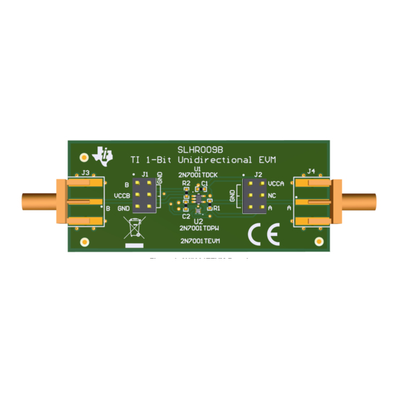
2N7001TEVM layout. Figure 3. 2N7001TEVM Layout Schematic and Bill of Materials Schematic Figure 4 shows the 2N7001TEVM schematic. The schematic includes the DCK and DPW package devices. Figure 4. 2N7001TEVM Schematic 2N7001T Evaluation Module SCEU013 – May 2018 Submit Documentation Feedback Copyright ©... -
Page 5: Bill Of Materials
Schematic and Bill of Materials www.ti.com Bill of Materials Table 1 lists the 2N7001TEVM bill of materials. Table 1. Bill of Materials Designator Qty Value Description Package Reference Part Number Manufacturer C1, C2 0.1uF CAP, CERM, 0.1 uF, 16 V, +/- 10%, X7R, 0402... - Page 6 STANDARD TERMS FOR EVALUATION MODULES Delivery: TI delivers TI evaluation boards, kits, or modules, including any accompanying demonstration software, components, and/or documentation which may be provided together or separately (collectively, an “EVM” or “EVMs”) to the User (“User”) in accordance with the terms set forth herein.
- Page 7 FCC Interference Statement for Class B EVM devices NOTE: This equipment has been tested and found to comply with the limits for a Class B digital device, pursuant to part 15 of the FCC Rules. These limits are designed to provide reasonable protection against harmful interference in a residential installation.
- Page 8 【無線電波を送信する製品の開発キットをお使いになる際の注意事項】 開発キットの中には技術基準適合証明を受けて いないものがあります。 技術適合証明を受けていないもののご使用に際しては、電波法遵守のため、以下のいずれかの 措置を取っていただく必要がありますのでご注意ください。 1. 電波法施行規則第6条第1項第1号に基づく平成18年3月28日総務省告示第173号で定められた電波暗室等の試験設備でご使用 いただく。 2. 実験局の免許を取得後ご使用いただく。 3. 技術基準適合証明を取得後ご使用いただく。 なお、本製品は、上記の「ご使用にあたっての注意」を譲渡先、移転先に通知しない限り、譲渡、移転できないものとします。 上記を遵守頂けない場合は、電波法の罰則が適用される可能性があることをご留意ください。 日本テキサス・イ ンスツルメンツ株式会社 東京都新宿区西新宿6丁目24番1号 西新宿三井ビル 3.3.3 Notice for EVMs for Power Line Communication: Please see http://www.tij.co.jp/lsds/ti_ja/general/eStore/notice_02.page 電力線搬送波通信についての開発キットをお使いになる際の注意事項については、次のところをご覧ください。http:/ /www.tij.co.jp/lsds/ti_ja/general/eStore/notice_02.page 3.4 European Union 3.4.1 For EVMs subject to EU Directive 2014/30/EU (Electromagnetic Compatibility Directive): This is a class A product intended for use in environments other than domestic environments that are connected to a low-voltage power-supply network that supplies buildings used for domestic purposes.
- Page 9 Notwithstanding the foregoing, any judgment may be enforced in any United States or foreign court, and TI may seek injunctive relief in any United States or foreign court. Mailing Address: Texas Instruments, Post Office Box 655303, Dallas, Texas 75265 Copyright © 2018, Texas Instruments Incorporated...
- Page 10 IMPORTANT NOTICE FOR TI DESIGN INFORMATION AND RESOURCES Texas Instruments Incorporated (‘TI”) technical, application or other design advice, services or information, including, but not limited to, reference designs and materials relating to evaluation modules, (collectively, “TI Resources”) are intended to assist designers who are developing applications that incorporate TI products;...
Need help?
Do you have a question about the 2N7001TEVM and is the answer not in the manual?
Questions and answers