Table of Contents
Advertisement
Safety Information ............................................................................................................................2
Electrostatic Discharge Sensitive (ESDS) Device Handling .........................................................2
Warranty .............................................................................................................................................2
Specifications .................................................................................................................................... 3
Speaker EQ Curves ..........................................................................................................................4
Theory of Operation ................................................................................................................... 5-21
Disassembly/Assembly Procedures ....................................................................................... 21-22
Test Procedures ........................................................................................................................ 23-30
Part List Notes ................................................................................................................................. 31
Main Part List, Digital BUILT-INvisible
Figure 1. Input/Output PCB, DSP PCB and Chassis Exploded View ............................................. 32
Figure 2. Amplifier PCB Assembly with Heatsink Exploded View .................................................. 33
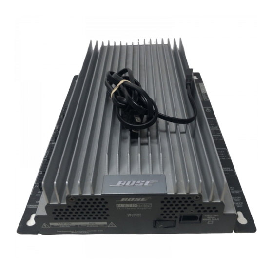
Figure 3. Assembled Amplifier with Heatsink Open ........................................................................ 34
Electrical Part Lists ................................................................................................................... 35-55
I/O PCB Electrical Part List ...................................................................................................... 35-41
DSP PCB Electrical Part List ................................................................................................... 42-48
Amplifier PCB Electrical Part List ........................................................................................... 49-55
Packaging Part List, Digital BUILT-INvisible System (see Figure 4) ........................................... 56
Figure 4. Digital BUILT-INvisible System Packaging View .............................................................. 56
Integrated Circuit Diagrams ..................................................................................................... 57-61
Appendix .................................................................................................................................... 62-80
Accessories used with the TA-1 Amplifier .............................................................................. 62-63
CD-50 System Assembly Part List ................................................................................................ 63
BUILT-INvisible Series II Bass Module ......................................................................................... 64
SE-1 Audio/Video Switcher ............................................................................................................ 65
Figure 5. SE-1 Audio/Video Switcher Packing Diagram ................................................................. 65
CI-1 Control Integrator ................................................................................................................... 66
Figure 6. CI-1 Control Integrator Packing Diagram ......................................................................... 66
Figure 7. TA-1 Amplifier Test Setup Diagram ................................................................................... 67
Figure 8. TA-1 Amplifier Connection Diagram ................................................................................. 68
Table 1. Satellite Speaker EQ DIP Switch Settings ........................................................................ 71
Computer Setup Procedure ..................................................................................................... 72-73
Amplifier Firmware Upgrade Procedure....................................................................................... 74
TA-1 Amplifier TAP Command Tables ..................................................................................... 75-78
System Troubleshooting Information ..................................................................................... 79-80
Figure 9. TS-200 System Connection Details ................................................................................. 81
Figure 10. TS-400 System Connection Details ............................................................................... 82
Figure 11. TS-600 System Connection Details ............................................................................... 83
CAUTION: The Bose
no user-serviceable parts. To prevent warranty infractions,
refer servicing to warranty service stations or factory service.
THIS DOCUMENT CONTAINS PROPRIETARY INFORMATION OF
BOSE CORPORATION WHICH IS BEING FURNISHED ONLY FOR THE
PURPOSE OF SERVICING THE IDENTIFIED BOSE PRODUCT BY AN
AUTHORIZED BOSE SERVICE CENTER OR OWNER OF THE BOSE
PRODUCT, AND SHALL NOT BE REPRODUCED OR USED FOR ANY
OTHER PURPOSE.
CONTENTS
®
Amplifier (see Figures 1, 2 and 3) ................................ 31
®
BUILT-INvisible
PROPRIETARY INFORMATION
1
®
TA-1 amplifier contains
Advertisement
Table of Contents

Subscribe to Our Youtube Channel
Related Manuals for Bose BUILT-INvisible TA-1


Summary of Contents for Bose BUILT-INvisible TA-1
-
Page 1: Table Of Contents
PROPRIETARY INFORMATION THIS DOCUMENT CONTAINS PROPRIETARY INFORMATION OF BOSE CORPORATION WHICH IS BEING FURNISHED ONLY FOR THE PURPOSE OF SERVICING THE IDENTIFIED BOSE PRODUCT BY AN AUTHORIZED BOSE SERVICE CENTER OR OWNER OF THE BOSE PRODUCT, AND SHALL NOT BE REPRODUCED OR USED FOR ANY OTHER PURPOSE. -
Page 2: Safety Information
• Transport or store ESDS devices in ESD protective bags, bins, or totes. Do not insert unprotected devices into materials such as plastic, polystyrene foam, clear plastic bags, bubble wrap or plastic trays. WARRANTY ® ® The Bose BUILT-INvisible TA-1 Theater Amplifier is covered by a 1-year transferable limited warranty... -
Page 3: Specifications
SPECIFICATIONS Power Output (all channels loaded): Bass Channel: 140 Watts at 100 Hz into 4 Ohms Satellite Channels: 35 Watts at 1 kHz into 8 Ohms Distortion: Bass Channel: < 0.4% THD at 0.5W Satellite Channels: < 0.1% THD at 0.5W Output Noise: Bass Channel: <... -
Page 4: Speaker Eq Curves
SPEAKER EQ CURVES CS-2 Satellite Speaker EQ Curve Jewel Cube ® Satellite Speaker EQ Curve Residential 131 ® Satellite Speaker EQ Curve Residential 1.2 Ohm Speakers EQ Curve Series II Bass Module ® ® VCS-10 Center Channel Speaker EQ Curve Acoustimass EQ Curve... -
Page 5: Theory Of Operation
II signal processing. It is intended for built in installations in ® Digital 5.1 decoding and Videostage Bose residential sound systems. Its six channels will normally be presenting sound for home theater, in 5.1 format. The Digital BUILT-Invisible amplifier has a total of six audio inputs:... - Page 6 THEORY OF OPERATION Input/Output (I/O) PCB (continued) S1 [A3] section 1, a user accessible switch, is used to connect the left and right inverting (–) pins of the Music Inputs together. S1-section 2 is used to connect the left and right – pins of the Video Inputs together.
- Page 7 THEORY OF OPERATION Input/Output (I/O) PCB (continued) Power supplies, +8V and +5V (continued) Until Q6 is turned on, the rest of the amplifier (the Power Amplifier and DSP PCBs) is off. The AC mains is applied to T5 [C1], rectified by D22 (full wave bridge), and filtered by C31. The +5V supply is created by U12 [C1] in a standard 3 terminal regulator application;...
- Page 8 ® amplifier. This connector serve two functions. It can be used for connection to a Bose Lifestyle music center or alternately for remote terminal access by means of an IBM compatible PC. A table will help explain this.
- Page 9 THEORY OF OPERATION Input/Output (I/O) PCB (continued) Power supply failure monitor level translator There are four power supplies on the power amplifier PCB, derived as two pairs of symmetrical bipolar supplies. By tying each of these supplies into a node by appropriate resistor values, we have a node that sits at zero volts when all supplies are normal.
- Page 10 THEORY OF OPERATION Digital Signal Processor (DSP) PCB (continued) Power Supplies There are several sets of internal power supply voltage rails. These voltages originate with the main power transformer located in the center of the Input/Output (I/O) PCB. There is also a small keep-alive transformer T5 [I/O PCB schematic, C1] located on the I/O board itself that allows the amplifier to be turned on by SmartSpeaker commands.
- Page 11 THEORY OF OPERATION Digital Signal Processor (DSP) PCB (continued) Microcontroller (continued) • to sequence the amplifier and codec mute lines as required. • to boot and monitor the performance of the DSPs. • and relay information to/from DSPs. In detail: 1.
- Page 12 THEORY OF OPERATION Digital Signal Processor (DSP) PCB (continued) Microcontroller (continued) 6. Other ADC ports are used for the following functions: • To monitor the gross DC offset on the five satellite speaker channels. Excessive DC offset is assumed to be an indication of a serious problem and the microcontroller will respond to this by shutting off the power to the amplifier.
- Page 13 THEORY OF OPERATION Digital Signal Processor (DSP) PCB (continued) Codec (continued) The codec generates three output signals, either from the 11.2896 MHz crystal, or from the input S/PDIF bitstream; • a serial bit stream containing the 20-bit audio data. • a bit_clock, which indicates when to sample the serial bit stream.
- Page 14 THEORY OF OPERATION Digital Signal Processor (DSP) PCB (continued) Signal Path The signal path through the system takes the following route(s): For analog signals, the L/R stereo pair is introduced from the source via the input cable from the Input/Output board and the 14-pin connector J9 [schematic sheet 1, A-D8]. Each signal is received pseudo-differentially by op-amp U105 [B/C6] and associated components and -6 dB of gain is applied to match with the maximum in/out signal level of the codec (1Vrms).
- Page 15 THEORY OF OPERATION Digital Signal Processor (DSP) PCB (continued) Power-Up Sequence (continued) The microcontroller proceeds to: • Set up its I/O ports. • Print out a “reset” message on the TTY output. • Program the codec and verify that it responds. •...
- Page 16 THEORY OF OPERATION Detailed Theory of Operation (see schematic diagram SD256431) Digital Signal Processor (DSP) Board, Sheet 1 of 4 (continued) The S/PDIF input enters the DSP board at J9 pin 10 [B8] and is routed to the codec by means of C151, R1, R2, D1, C1, C7 and R5 [B5].
- Page 17 THEORY OF OPERATION Detailed Theory of Operation (see schematic diagram SD256431) Digital Signal Processor (DSP) Board, Sheet 1 of 4 (continued) Analog output buffers consists of U103, U104 [B-D2], and associated components. Gain is set by the ratio of R132 to R131 [D2]; to about 6x. Note that the ratio of R189 to R188 [D2] must match.
- Page 18 THEORY OF OPERATION Detailed Theory of Operation (see schematic diagram SD256431) Digital Signal Processor (DSP) Board, Sheet 2 of 4 (continued) Q200 [C2] allows the microcontroller to pull down on the DSP’s reset line. When the microcontroller first boots, all of its output ports are set to a high impedance state. Q200 remains turned on by R252, which holds the DSPs in reset, until the microcontroller is ready to boot the DSPs.
- Page 19 THEORY OF OPERATION Detailed Theory of Operation (see schematic diagram SD256431) Digital Signal Processor (DSP) Board, Sheet 4 of 4 (continued) C506 [D3] is the “soft-start” capacitor, which forces the regulator to start up slowly when power is first applied, thus limiting the inrush current. R510 and Q500 [D3] allow the “soft-start” pin to be pulled low, shutting off the regulator.
- Page 20 THEORY OF OPERATION Detailed Theory of Operation (see schematic diagram SD256421) Power Amplifier Board, Bass Channel Power Amplifier (continued) Short circuit protection is provided through current sense resistor R822. At greater than 16A, Q726 conducts and triggers the one-shot op-amp circuit U707, pins 5, 6 and 7, and mutes the amp for several seconds.
-
Page 21: Disassembly/Assembly Procedures
THEORY OF OPERATION Power Amplifier Board, Sheet 2 of 2 (continued) Outputs to the DSP board from the amplifier board at J700 also include the +20Vdc at pin 4 through fusible resistor R704 [C6] to create +20 fused. The mute and standby signals for the power amplifiers are brought into the amplifier board at J700 on pins 15, 16 and 18. - Page 22 DISASSEMBLY/ASSEMBLY PROCEDURES 4.3 Align the power transformer (4) with the 8. Amplifier Board Replacement chassis and secure it in place using the hex head bolt (2) removed in step 3.3. 8.1 Place the thermal conducting insulating tape strips (15) onto the heatsink (16) where 4.4 Perform procedure 2.
-
Page 23: Test Procedures
S/PDIF Analog to Digital Converter CAT-5 Cable with RJ-45 connectors Note: These commands are case 75 Ohm RCA to RCA S/PDIF video cable sensitive. ® Bose Digital Source plate IBM Compatible PC w/Windows ® - ICA (selects music audio inputs) TAP Cable... - Page 24 TEST PROCEDURES Music Audio Tests 1.15 Apply a 1.8 Vrms, 1 kHz signal to the left music audio input at J6 pins 1 and 2. 1. Front Channel Audio Tests 1.16 Measure the compressor signal distor- 1.1 Set up the amplifier under test as outlined tion level at the left front speaker output at in the test setup.
- Page 25 TEST PROCEDURES 2.11 Apply an in-phase, 50 mV, 1 kHz signal 3.7 Measure the output level at the left and to the left and right music audio inputs at J6. right surround channel speaker outputs at J14. It should be +36.9 dB + 1.5 dB. 2.12 Measure the small signal distortion level at the center channel speaker output 3.8 Apply a L= -R, 100 mV, 12 kHz signal to...
- Page 26 TEST PROCEDURES 4.4 Measure the output level at the bass 4.16 Measure the compressor signal distor- channel speaker output at J15 pins 1 and 2. tion level at the bass channel speaker output It should be +38.4 dB + 1.5 dB. at J15 pins 1 and 2.
- Page 27 7.4 Apply a 100 mV, 1 kHz signal to the left input jack video audio input at J21 pins 1 and 2. BOSE 7.5 Reference a dB meter to the input level. 7.6 Measure the output level at the left front speaker output at J12 pins 3 and 4.
- Page 28 TEST PROCEDURES 8.3 Verify that the TA-1 center channel output 10. Relay K1 Test at J13 pins 1 and 2 is +33.7 dB + 1.5 dB. Note: Music Center Input pins 1 and 2 of J8 8.4 Move the output of the A/D converter (normally used for the 10 Vdc turn-on and to the Digital Source 2 input of the Digital serial data input from the music center) can...
- Page 29 TEST PROCEDURES 11. DSP Board Tests 11.8 Issue one 5 SPEAKER mode com- mand (I38). Confirm that the TA-1 amplifier is Note: These tests will verify that the DSP now in 5 channel mode. board is working properly. 11.9 Issue one SURROUND UP command Note: If you are performing these tests (ID0).
- Page 30 TEST PROCEDURES 11.22 Issue one 1:5 ON mode command 13.34 Issue one VIDEO 1 mode command (I20). Confirm that the 1:5 processing is on. (I70). Confirm that the FEQ and DRC are on. 11.23 Issue one 1:5 OFF mode command 13.35 Issue one VIDEO 2 mode command (IA0).
-
Page 31: Part List Notes
PART LIST NOTES 1. This part is not normally available from Customer Service. Approval from the Field Service Manager is required before ordering. 2. The individual parts located on the PCBs are listed in the Electrical Part List. This part is critical for safety purposes. Failure to use a substitute replacement with the same safety characteristics as the recommended replacement part might create shock, fire and/or other hazards. - Page 32 Note: This cable is soldered directly to the I/O PCB. Figure 1. Input/Output PCB, DSP PCB and Chassis Exploded View...
- Page 33 Figure 2. Amplifier PCB Assembly with Heatsink Exploded View...
- Page 34 Figure 3. Assembled Amplifier with Heatsink Open...
-
Page 35: Electrical Part Lists
I/O PCB ELECTRICAL PART LIST Resistors Reference Description Part Number Note Designator 5K, RESNET, SOIC 16, 1/10W, 1% 250124-5001 5K, RESNET, SOIC 16, 1/10W, 1% 250124-5001 5K, RESNET, SOIC 16, 1/10W, 1% 250124-5001 5K, RESNET, SOIC 16, 1/10W, 1% 250124-5001 4.99K, 0805, 1/10W, 1% 133625-4991 2K, 0805, 1/10W, 1%... - Page 36 I/O PCB ELECTRICAL PART LIST Resistors (continued) Reference Description Part Number Note Designator 10 OHM, 0805, 1/10W, 1% 133625-10R0 10 OHM, 0805, 1/10W, 1% 133625-10R0 10 OHM, 0805, 1/10W, 1% 133625-10R0 10 OHM, 0805, 1/10W, 1% 133625-10R0 10 OHM, 0805, 1/10W, 1% 133625-10R0 100 OHM, 0805, 1/10W, 1% 133625-1000...
- Page 37 I/O PCB ELECTRICAL PART LIST Resistors (continued) Reference Description Part Number Note Designator R120 1.0K, 1206, 1/8W, 1% 124894-1001 R121 100K, SM, 0805, 1/10W, 1% 133625-1003 R122 100K, SM, 0805, 1/10W, 1% 133625-1003 R123 1K, 0805, 1/10W, 1% 133625-1001 R124 100K, SM, 0805, 1/10W, 1% 133625-1003 R125...
- Page 38 I/O PCB ELECTRICAL PART LIST Capacitors (continued) Reference Description Part Number Note Designator 1000pF, 0805, X7R, 50V, 10% 133623-102 270pF, 0805, C0G, 50V, 5% 133622-271 .033uF, 0805, X7R, 50V, 5% 133623-3335 .1uF, SM, 0805, X7R, 50V, 10% 133623-104 .1uF, SM, 0805, X7R, 50V, 10% 133623-104 270pF, 0805, C0G, 50V, 5% 133622-271...
- Page 39 I/O PCB ELECTRICAL PART LIST Diodes Reference Description Part Number Note Designator ZENER, SOT23, 7.5V 261419 DUAL, BAV99R-R, SOT23 147239 LED, TH, 3MM, IR, 1.2V 256474 DUAL, BAV99R-R, SOT23 147239 DUAL, BAV99R-R, SOT23 147239 DUAL, BAV99R-R, SOT23 147239 DUAL, BAV99R-R, SOT23 147239 DUAL, BAV99R-R, SOT23 147239...
- Page 40 I/O PCB ELECTRICAL PART LIST Integrated Circuits Reference Description Part Number Note Designator OP AMP, DUAL, SO8, NJM5532M-TE2 256429 OP AMP, DUAL, SO8, NJM5532M-TE2 256429 CMOS ANALOG MUX, DUAL 4-CHANNEL, 256483 DG409CY MICRO RESET CIRCUIT, SOT23, 250096 MAX809JEUR MICRO, PROGRAMMED, PIC16F877 256469-001 SERIAL EEPROM, 128X8 BIT, SOIC8, 24C01A 184044...
- Page 41 I/O PCB ELECTRICAL PART LIST Miscellaneous (continued) Reference Description Part Number Note Designator HDR, PCB MNT, 3 POS, SERIAL I/O, 177291-03 TV&EXT PWR HDR, PCB MNT, 5 POS, L&R A IN, L&R V IN, 177291-05 IR I/O HDR, PCB MNT, 3 POS, SERIAL I/O, 177291-03 TV&EXT PWR HDR, PCB MNT, 4 POS, LIFESTYLE INPUT,...
-
Page 42: Dsp Pcb Electrical Part List
DSP PCB ELECTRICAL PART LIST Resistors Reference Description Part Number Note Designator 100 OHM, 0805, 1/10W, 5% 133626-1015 2 OHM, 0805, 1/10W, 5% 133626-2R05 30 OHM, 1206, 1/8W, 5% 124895-3005 100 OHM, 0805, 1/10W, 5% 133626-1015 3.48K, 0805, 1/10W, 1% 133625-3481 6.19K, 0805, 1/10W, 1% 133625-6191... - Page 43 DSP PCB ELECTRICAL PART LIST Resistors (continued) Reference Description Part Number Note Designator R168 100K, 0805, 1/10W, 5% 133626-1045 R169 100K, 0805, 1/10W, 5% 133626-1045 R170 100K, 0805, 1/10W, 5% 133626-1045 R171 100K, 0805, 1/10W, 5% 133626-1045 R175 1.0 M, 0805, 1/10W, 1% 133625-1004 R176 2 OHM, 0805, 1/10W, 5%...
- Page 44 DSP PCB ELECTRICAL PART LIST Resistors (continued) Reference Description Part Number Note Designator R257 300 OHM, 0805, 1/10W, 5% 133626-3015 R260 1.00K, CHIP, 0805, 1/10W, 1% 133625-1001 R261 10.0K, 0805, 1/10W, 5% 133626-1035 R262 1.00K, 0805, 1/10W, 1% 133625-1001 R263 30K, 0805, 1/10W, 5% 133626-3035 R265...
- Page 45 DSP PCB ELECTRICAL PART LIST Capacitors (continued) Reference Description Part Number Note Designator 1.0uF, 1206, X7R, 25V, 10% 262063-105 C100 3300pF, 0805, X7R, 50V, 10% 133623-332 C102 330pF, 0805, COG, 50V, 5% 133622-331 C103 100pF, 0805, COG, 50V, 5% 133622-101 C104 10uF, EL, 85C, 25V, 20% 149947-100E...
- Page 46 DSP PCB ELECTRICAL PART LIST Capacitors (continued) Reference Description Part Number Note Designator C206 33pF, 0805, COG, 50V, 5% 133622-330 C207 1.0uF, 1206, X7R, 25V, 10% 262063-105 C208 1.0uF, 1206, X7R, 25V, 10% 262063-105 C209 1000pF, 0805, COG, 50V, 5% 133622-102 C211 330pF, 0805, COG, 50V, 5%...
- Page 47 DSP PCB ELECTRICAL PART LIST Inductors Reference Description Part Number Note Designator 400 OHMS, CHIP, 0805 188587-401 400 OHMS, CHIP, 0805 188587-401 L200 400 OHMS, CHIP, 0805 188587-401 L500 100uH, FIXED, SMT, 20% 251161-101 L501 22uH, SMD, 20% 173273-220 Diodes Reference Description Part Number...
- Page 48 DSP PCB ELECTRICAL PART LIST Integrated Circuits Reference Description Part Number Note Designator L78M05, VOLT REG, 5V, DPAK 197227-001 U100 CS4226-KQ, CODEC 197221 U101 74LCX244, OCTAL BUFFER, 3V 193841-001 U102 74ACT244, OCTAL BUFFER 193842-001 U103 TLO74D, QUAD OP AMP, SOIC 186112 U104 TLO74D, QUAD OP AMP, SOIC...
-
Page 49: Amplifier Pcb Electrical Part List
AMPLIFIER PCB ELECTRICAL PART LIST Resistors Reference Description Part Number Note Designator R700 22.1K, 1206, 1/8W, 1% 124984-2212 R701 274K, 1206, 1/8W, 1% 124894-2743 R702 1.50K, 1206, 1/8W, 5% 124895-1525 R703 1.50K, 1206, 1/8W, 5% 124895-1525 R704 5.1 OHM, FUSING, 2W, 5% 170174-5R1 R705 1.50K, 1206, 1/8W, 5%... - Page 50 AMPLIFIER PCB ELECTRICAL PART LIST Resistors (continued) Reference Description Part Number Note Designator R743 100K, 1206, 1/8W, 5% 124895-1045 R744 100K, 1206, 1/8W, 5% 124895-1045 R745 1.0K, 1206, 1/8W, 5% 124895-1025 R746 10.0K, 1206, 1/8W, 5% 124895-1035 R747 1.0K, 1206, 1/8W, 5% 124895-1025 R748 2.49K, 1206, 1/8W, 1%...
- Page 51 AMPLIFIER PCB ELECTRICAL PART LIST Resistors (continued) Reference Description Part Number Note Designator R789 200K, 1206, 1/8W, 1% 124894-2003 R790 16.5K, 1206, 1/8W, 1% 124894-1652 R791 1 MEG, 1206, 1/8W, 5% 124895-1055 R792 1.0K, 1206, 1/8W, 5% 124895-1025 R793 4.22K, 1206, 1/8W, 1% 124894-4221 R794 301 OHM, 1206, 1/8W, 1%...
- Page 52 AMPLIFIER PCB ELECTRICAL PART LIST Capacitors Reference Description Part Number Note Designator C700 .01uF, 0805, X7R, 50V, 10% 133623-103 C701 .01uF, 0805, X7R, 50V, 10% 133623-103 C702 1uF, ALUM EL, SM, 85C, 50V, 20% 177902-010H C703 .01uF, 0805, X7R, 50V, 10% 133623-103 C704 1uF, ALUM EL, SM, 85C, 50V, 20%...
- Page 53 AMPLIFIER PCB ELECTRICAL PART LIST Capacitors (continued) Reference Description Part Number Note Designator C748 1000pF, 1206, COG, 50V, 10% 124956-1022 C749 1000pF, 1206, COG, 50V, 10% 124956-1022 C750 1000pF, 1206, COG, 50V, 10% 124956-1022 C751 .01uF, 1206, X7R, 25V, 5% 131754-103 C752 .01uF, 1206, X7R, 25V, 5%...
- Page 54 AMPLIFIER PCB ELECTRICAL PART LIST Diodes Reference Description Part Number Note Designator B700 RECTIFIER, BRIDGE, 100V, 6A 187611 B701 RECTIFIER, BRIDGE, 100V, 6A 187611 D701 ZENER, 5.6V, 225MW, 1N5232 135247-5232 D702 DUAL, SOT-23, BAV99 147239 D703 ZENER, 5.6V, 225MW, 1N5232 135247-5232 D704 1N5402...
- Page 55 AMPLIFIER PCB ELECTRICAL PART LIST Transistors (continued) Reference Description Part Number Note Designator Q719 DARL, N, 80V, 25A, SGSD100 197593 Q720 DARL, N, 80V, 25A, SGSD100 197593 Q721 PNP, 55V, 150mA, SOT-23 134743 Q722 NPN, SOT-23, 2SC2812 134741 Q723 PNP, 55V, 150mA, SOT-23 134743 Q724 JFET, SOT, MMBF4392...
-
Page 56: Packaging Part List, Digital Built-Invisible System (See Figure 4)
PACKAGING PART LIST Digital BUILT-INvisible ® System (see Figure 4) Item Description Part Qty. Note Number Number KIT, INSTALLATION HARDWARE, DBIS 261442 CONSISTS OF: SCREW, MACH, #10-24X2.5, PAN, XREC 188409 TOGGLE WINGS, #10-24, STEEL 179296 SCREW, TAPP, #10X16, PAN, XREC, 2 197892-009 PACKING, ENDCAP, FOAM 172063... -
Page 57: Integrated Circuit Diagrams
6. B Inverting Input 5. N.C. 4. SVR 7. B Output 3. Non-Inverting Input 8. V+ 2. Inverting Input 1. Stand-by Gnd. Bose P/N: 146820, Dual Op-amp, NJM2082 TOP-VIEW +Vs (signal) +Vs (power) Pin Function 1. A Output TDA7294 2. A Inverting Input 3. - Page 58 Output remains low while Vcc is below the reset Top View threshold, and for a period of time after Vcc rises RESET above the reset threshold. 3. Vcc Supply voltage Bose P/N: 191158-01, Reset IC, MAX809 Bose P/N: 193841-001, Octal Buffer, 74LCX244...
- Page 59 INTEGRATED CIRCUIT DIAGRAMS Bose ® P/N: 193842-001, Octal Buffer, 74ACT244 Bose P/N: 193834, DSP Pinout Diagram, Bose P/N: 193846-001, Voltage Regulator, ADSP21061LKS-160 SMPS Bose P/N: 193834, DSP Pin Assignment Table, ADSP21061LKS-160...
- Page 60 INTEGRATED CIRCUIT DIAGRAMS Bose ® P/N: 193858-001, Quad Nand Gate, MC74CLX00 Bose P/N: 197221, Codec, CS4226KQ Bose P/N: 196670-001, JK Flop, 74HC73 Bose P/N: 197227, Voltage Regulator, 5 Volt, Bose P/N: 261415, PIC16F877, I/O Micro DPAK, LM7805...
- Page 61 INTEGRATED CIRCUIT DIAGRAMS ® Bose P/N: 253903-32, Microprocessor, Bose P/N: 256483, Analog MUX, DG409CY, TMP87PH47U Pinout Diagram Bose P/N: 256483, Analog MUX, DG409CY, Schematic Diagram Bose P/N: 261421, AND Gate, SN74ACH1G08 Bose P/N: 261417, RS-232 Transceiver, MAX202CSE...
-
Page 62: Appendix
Appendix Accessories used with the TA-1 amplifier Product Description Product Code ® BUILT-INvisible TA-1 theater amplifier 027356 Audio/Video Integration Accessories – for use with TA-1 amplifier SE-1 System Expander 027574 CI-1 Control Integrator 027595 TA-1 Remote 027701 Coaxial to RJ45 adapter 027575 IR Sensor 027700... -
Page 63: System Assembly Part List
Appendix Accessories used with the TA-1 amplifier (continued) Product Description Product Code Music Source Accessories Antenna Kit 002140 CD-20 Six disc magazine 016693 Installation Accessories Digital Source Plate (white, Decora) 027573 Source Plate (white, Decora) 026230 MRI/CD20 source connection cable -- 8 pin male mini-DIN to 8 pin male mini- 026224 DIN, all pins connected Fixed source cable, 7 feet -- 2 male RCA’s to 8 pin male mini-DIN... -
Page 64: Built-Invisible Series Ii Bass Module
® BUILT-INVISIBLE SERIES II BASS MODULE Item Number Description Part Number Note 187232-003 Conn, Binding Post, Model 203 , Gray Screw, Tapp, 8-11 x .75, PAN, XRC/SQ 172672-12 Insert, Packing 259825 Bag, Poly, 23 x 44 x 10.5 x 1.25 mil 100652 Packing, Corner Post 130759... -
Page 65: Audio/Video Switcher
SE-1 AUDIO/VIDEO SWITCHER Item Description Part Number Qty. Number POWER PACK, 12 VDC, 500 mA VENDOR SUPPLIED CABLE ASSY, IR SENSOR 260074-1 CABLE ASSY, SOURCE, 7 FT. 257180 CABLE ASSY, 3.5mm TO 8 PIN MINI DIN, 6 FT. 261489 CABLE ASSY, S-VIDEO, 6 FT. VENDOR SUPPLIED CABLE ASSY, COMPOSITE VIDEO, 6 FT. -
Page 66: Control Integrator
CI-1 CONTROL INTEGRATOR Item Description Part Number Qty. Number POWER PACK, 12 VDC, 500 mA VENDOR SUPPLIED CABLE ASSY, IR SENSOR 260074-1 CABLE ASSY, SOURCE, 3.5mm to 3.5mm, 6 FT. 260073 CABLE ASSY, SOURCE, 3.5mm to 3.5mm, 7 FT. 260075 CI-1 CONTROL INTEGRATOR VENDOR SUPPLIED CI-1 INSTALLATION GUIDE... - Page 67 Appendix Figure 7. TA-1 Amplifier Test Setup Diagram...
- Page 68 Appendix LEFT + J6-1 LEFT - J6-2 J12-4 LEFT FRONT MUSIC SATELLITE GROUND J6-3 J12-3 BLACK AUDIO INPUT RIGHT + J6-4 J12-2 RIGHT FRONT SATELLITE RIGHT - J6-5 J12-1 BLACK BALANCED/ UNBALANCED INPUT SWITCH SPEAKER LEFT + J21-1 SELECTOR SWITCH S4 LEFT - J21-2 VIDEO...
- Page 69 These controls are for room-specific equalization only. They are not intended to be adjusted by the customer. They are normally set once by the system installer and then left at that setting for that installation. These commands are not supported on the Bose ®...
- Page 70 Appendix Switches There are three sets of switches on the TA-1 amplifier; the speaker selector set, the mode set, and the balanced input set. Speaker selector switches These switches are used to set the EQ for various speaker configurations. Refer to "Setting the speaker configuration DIP switches"...
- Page 71 Appendix Setting the speaker configuration DIP switches (continued) Important: Be sure to select the right settings for the speaker configuration you are using from the table below. If an error is made, the speakers will have the wrong equalization and will not sound right when played.
-
Page 72: Computer Setup Procedure
Appendix Computer Setup Procedure Use this procedure to configure your IBM compatible PC for communication with the digital bass module. 1. Open a terminal window, as shown at right, in either Terminal or Hyperterm, as applicable for the version of Microsoft ®... - Page 73 Appendix Computer Setup Procedure (continued) 4. In the Test Properties dialog box, click on the Settings tab and set the controls as shown in the example at right. Note: Be sure to check “Beep three times when connecting or disconnecting”. 5.
-
Page 74: Amplifier Firmware Upgrade Procedure
Appendix Amplifier Firmware Upgrade Procedure TAP Cable build instructions Obtain a female DB9 9 pin D-Sub connector. Obtain a 3 pin connector, part number 172930-3. This is the same connector as used for the Serial I/O and TV Sense inputs to the TA-1 amplifier. Obtain 3 different colored 18 AWG wires. -
Page 75: Amplifier Tap Command Tables
Appendix TAP Commands Table These commands are used to control the TA-1 amplifier. You will need to configure your IBM compatible PC for a hyperterminal session as outlined earlier in the appendix. You will also need to construct a TAP cable using the instructions on the previous page. Command Format Command: single ASCII character (case sensitive) Argument: 0-5 ASCII characters, command dependant... - Page 76 Appendix Serial Commands to the TA-1 amplifier (continued) Description Cmnd Arg Values Action Notes/Examples Ack enable P = 0,1 Enables or A1<CR> = or disable disables Acknowledge enabled Command A0<CR> = Acknowledgem Acknowledge disabled ents Acknowledge = ‘>’ if cmnd ok Acknowledge = ‘?’...
- Page 77 Appendix Serial Commands to the TA-1 amplifier (continued) Description Cmnd Arg Values Action Notes/Examples Version none Displays V<CR> Displays display software software version version number Display <CR> Five character Displays unit N<CR> Displays serial serial serial number serial number number number (ASCII) Plant Code...
- Page 78 Appendix IR Commands Table Index/ Description Index/ Description DATA DATA (HEX) KEY # (HEX) KEY # Mute Vol Down Vol Up 1:5 On 1:5 Off AM/FM Random disc Mute Off Stereo Center - Center + Treble Middle Surround - Surround Surround + Stereo + Center Treble +...
-
Page 79: System Troubleshooting Information
Appendix System Troubleshooting Information Use the table below to troubleshoot SE-1 system expander setup problems. Keep in mind that a symptom listed near the end of this table may be caused by problems addressed earlier in the table. Symptoms Possible cause What to check or try •... - Page 80 Appendix System Troubleshooting Information (continued) Symptoms Possible cause What to check or try • Amp responds to Amp may be off. The An ON command has been issued. volume buttons amp will not respond (command LEDs to volume commands blink) but there is no unless it is on.
- Page 84 ® BUILT-INvisible TA-1 Theater Amplifier Service Manual © 2002 Bose Corporation Part Number Rev. 00 263494...
- Page 85 SPECIFICATIONS AND FEATURES SUBJECT TO CHANGE WITHOUT NOTICE Bose Corporation The Mountain Framingham Massachusetts USA 01701 P/N: 263494 Rev. 00 6/2002 (H) FOR TECHNICAL ASSISTANCE OR PART ORDERS, CALL 1-800-233-4408 http://serviceops.bose.com...
Need help?
Do you have a question about the BUILT-INvisible TA-1 and is the answer not in the manual?
Questions and answers