Bose FreeSpace DXA 2120 Service Manual
Digital mixer/amplifier
Hide thumbs
Also See for FreeSpace DXA 2120:
- Installation and operation manual (56 pages) ,
- Owner's manual (16 pages)

Related Manuals for Bose FreeSpace DXA 2120


Summary of Contents for Bose FreeSpace DXA 2120
- Page 1 ® FreeSpace DXA 2120 Digital Mixer/Amplifier (US and non-US units) ©2010 Bose Corporation Service Manual Reference Number 294962-SM Rev. 01 Electronic Copy Only...
-
Page 2: Table Of Contents
DXA 2120 Amplifier/Mixer (see Figure 1) ......11 Figure 1. FreeSpace DXA 2120 Packaging View ................11 Main Part List, FreeSpace DXA 2120 Amplifier/Mixer (see Figure 2) ......... 12 Figure 2. FreeSpace DXA 2120 Amplifier/Mixer Exploded View ............13 Electrical Part Lists ........................14-52 Control PCB Assembly ...................... -
Page 3: Safety Information
BY AN AUTHORIZED BOSE SERVICE CENTER OR OWNER OF THE BOSE PRODUCT, AND SHALL NOT BE REPRODUCED OR USED FOR ANY OTHER PURPOSE. WARRANTY The Bose FreeSpace DXA 2120 Digital Mixer/Amplifier is covered by a limited 2-year transfer- able limited warranty. -
Page 4: Product Description
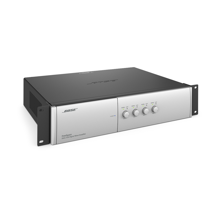
Product Description ® ® The Bose FreeSpace DXA 2120 Digital Mixer/Amplifier integrates digital signal POWER processing with two 120-watt output channels. Designed as a mixer/router for business music applications, it features an LCD panel and control buttons behind the front cover for ready access and easy configura- tion. - Page 5 Hardware Description Front panel with open compartment 9 10 System Controls 7 - Bass and Treble knobs - Adjust tonal 1 - LCD panel - Displays menu selection for balance for OUTPUT 1 and OUTPUT 2. configuring and viewing system settings. 2 - Directional buttons - Navigate system Control Compartment menus and setting options as shown on the...
- Page 6 Euroblock input jacks.) The FreeSpace ® DXA 2120 is designed to be 3 - INPUT 2 of 4 - Balanced Euroblock audio compatible with the following Bose user input jack. interfaces: 4 - DIRECT INPUT - Balanced override input •...
- Page 7 System Setup This section provides instructions on setting • When the system is unlocked, you can the system for preferred operation. To make navigate to system setup options. these settings, the system must be con- • Use the arrow and SELECT buttons to nected to power and the AC POWER switch move through the menus and change set to ON.
-
Page 8: Specifications
Specifications Audio Inputs Mic Inputs (4 - Balanced): Connectors: 3-pin Euroblock Input Range: 20 - 20kHz Input Impedance: 2k ohms (Mic) 25k ohms (Line) Equivalent Input Noise: -122dB Line Inputs (4 - Unbalanced): Connectors: Dual RCA (summed to mono) Input Range: 20 20kHz Input Impedance: 10k ohms... - Page 9 Specifications (continued) A/D and D/A Converters: 24-bit Communication Port: RS-232 serial port LED Status Indicators: Power - blue; Signal present - green; Clip - red Power Mains Voltage: 100 to 240VAC; 50 to 60Hz AC Power Consumption: Idle: Active: 350W Fuse Type: 120V T6.3A/250 or 240V T3.15A/250 L DC Backup Power:...
-
Page 10: Electrostatic Discharge Sensitive (Esds) Device Handling
ELECTROSTATIC DISCHARGE SENSITIVE (ESDS) DEVICE HANDLING This unit contains ESDS devices. We recommend the following precautions when repairing, replacing or transporting ESDS devices: • Perform work at an electrically grounded work station. • Wear wrist straps that connect to the station or heel straps that connect to conductive floor mats. -
Page 11: Dxa 2120 Amplifier/Mixer (See Figure 1)
– MIC/LINE CONN, 3 POS 2113-3143+0 – DIRECT/PAGE CONN, 4 POS 2113-3147+0 – RMT INPUT CONN, 6 POS 2113-3149+0 – AUX OUTPUT CONN, 3 POS 2113-3143+0 – SPKR OUTPUT CONN, 5 POS 2113-3272+0 Figure 1. FreeSpace DXA 2120 Packaging View... -
Page 12: Main Part List, Freespace Dxa 2120 Amplifier/Mixer (See Figure 2)
MAIN PART LIST FreeSpace ® DXA 2120 Amplifier/Mixer (see Figure 2) ® Item Description Vendor Part Number Bose Qty. Note Number Part Number TOP COVER, CHASSIS 1405-8601+0 298705 DSP/MCU PCB ASSEMBLY SVC-MIXER14+DSP 298689 BRACKET FOR DSP PCB 4135-6371+0 POWER SUPPLY PCB ASSY... - Page 13 AC POWER SWITCH 5200-4942+0 RIBBON CABLE 7012-7870+0 298688 LCD DISPLAY 8902-0005+0 298686 FUSE T6.3A 250V 5X20 UL 5120-0040+0 177311- (120V UNITS) 06300 FUSE T3.15A 250V 5X20MM 5120-0079+0 177311- UR & SEMKO (220-240V) 03150 Figure 2. FreeSpace DXA 2120 Amplifier/Mixer Exploded View...
-
Page 14: Electrical Part Lists
ELECTRICAL PART LIST Control PCB Assembly Resistors Reference Description Vendor Part Note Designator Number R401 100 OHM, RCF, 1/4W, 5%, ATS 4705-101J+C R402 100 OHM, RCF, 1/4W, 5%, ATS 4705-101J+C R403 100 OHM, RCF, 1/4W, 5%, ATS 4705-101J+C R404 100 OHM, RCF, 1/4W, 5%, ATS 4705-101J+C R405 100 OHM, RCF, 1/4W, 5%, ATS... - Page 15 ELECTRICAL PART LIST Control PCB Assembly LEDs Reference Description Vendor Part Note Designator Number LED401 LED, SLR342-MG3F, GN (ROHM) 3700-2570+G LED402 LED, SLR342-MG3F, GN (ROHM) 3700-2570+G LED403 LED, SLR342-MG3F, GN (ROHM) 3700-2570+G LED404 LED, SLR342-MG3F, GN (ROHM) 3700-2570+G LED405 LED, CY, D3X8, GN 3700-3616+G LED406 LED, CY, D3X8, GN...
- Page 16 ELECTRICAL PART LIST Control PCB Assembly Miscellaneous (continued) Reference Description Vendor Part Note Designator Number LCD401 HEADER, 16P, P2.54, ST, MALE 2101-3141+0 \LED401 LED SPACER, H=12.0MM 4171-0081+0 \LED402 LED SPACER, H=12.0MM 4171-0081+0 \LED403 LED SPACER, H=12.0MM 4171-0081+0 \LED404 LED SPACER, H=12.0MM 4171-0081+0 \LED405 LED SPACER, H=8.5MM...
-
Page 17: Dc24 Pcb Assembly
ELECTRICAL PART LIST DC24 PCB Assembly Resistors Reference Description Vendor Part Qty. Note Designator Number R701 100 OHM, RCF, 1/4W, 5%, ATS 4705-101J+C R702 10K, RCF, 1/4W, 5%, ATS 4705-103J+C R703 15K, RCF, 1/4W, 5%, ATS 4705-153J+C R704 4.7K, RCF, 1/4W, 5%, ATS 4705-472J+C R705 4.7K, RCF, 1/4W, 5%, ATS... - Page 18 Note Designator Number T701 TRANSFORMER, DC-DC, 24V, 150W, 1806-3933+0 24VX2, 15VX2 FUSE, T10AH, 250V 5120-0110+0 F701 ® (BOSE PART NUMBER 325634-0010) F701A FUSE HOLDER 4132-1011+0 F701B FUSE HOLDER 4132-1011+0 WIRE-CONN, 1P, #18, UL1015, L=300, 7012-7832+0 BLK, 250-TERMINAL WIRE-CONN, 1P, #18, UL1015, L=250,...
-
Page 19: Digital Signal Processor (Dsp) Pcb Assembly
ELECTRICAL PART LIST Digital Signal Processor (DSP) PCB Assembly Resistors Reference Description Vendor Part Number Note Designator R201 1K, RMG, 1/16W, 5%, 0603/1608 4723-102J+P R202 1K, RMG, 1/16W, 5%, 0603/1608 4723-102J+P R203 10K, RMG, 1/16W, 5%, 0603/1608 4723-103J+P R204 10K, RMG, 1/16W, 5%, 0603/1608 4723-103J+P R205 1K, RMG, 1/16W, 5%, 0603/1608... - Page 20 ELECTRICAL PART LIST Digital Signal Processor (DSP) PCB Assembly Resistors (continued) Reference Description Vendor Part Number Note Designator R265 1K, RMG, 1/16W, 5%, 0603/1608 4723-102J+P R266 1K, RMG, 1/16W, 5%, 0603/1608 4723-102J+P R267 10K, RMG, 1/16W, 5%, 0603/1608 4723-103J+P R268 10K, RMG, 1/16W, 5%, 0603/1608 4723-103J+P R269...
- Page 21 ELECTRICAL PART LIST Digital Signal Processor (DSP) PCB Assembly Resistors (continued) Reference Description Vendor Part Number Note Designator R318 10 OHM, RMG, 1/16W, 5%, 0603/1608 4723-100J+P R320 10K, RMG, 1/16W, 5%, 0603/1608 4723-103J+P R321 10K, RMG, 1/16W, 5%, 0603/1608 4723-103J+P R322 10K, RMG, 1/16W, 5%, 0603/1608 4723-103J+P...
- Page 22 ELECTRICAL PART LIST Digital Signal Processor (DSP) PCB Assembly Capacitors Reference Description Vendor Part Number Note Designator C201 0.1uF, CC, 50V, 10%, 0603/1608, 1x2 150F-104K+P-AC C202 0.1uF, CC, 50V, 10%, 0603/1608, 1x2 150F-104K+P-AC C203 10uF, CE, 16V, 20%, RLT, 4x7, NICHICON 157D-106M+K-GMK C204 0.1uF, CC, 50V, 10%, 0603/1608, 1x2...
- Page 23 ELECTRICAL PART LIST Digital Signal Processor (DSP) PCB Assembly Capacitors (continued) Reference Description Vendor Part Number Note Designator C246 10uF, CE, 16V, 20%, RLT, 4x7, NICHICON 157D-106M+K-GMK C247 0.1uF, CC, 50V, 10%, 0603/1608, 1x2 150F-104K+P-AC C248 10uF, CE, 16V, 20%, RLT, 4x7, NICHICON 157D-106M+K-GMK C249 0.1uF, CC, 50V, 10%, 0603/1608, 1x2...
- Page 24 ELECTRICAL PART LIST Digital Signal Processor (DSP) PCB Assembly Capacitors (continued) Reference Description Vendor Part Number Note Designator C300 0.1uF, CC, 50V, 10%, 0603/1608, 1x2 150F-104K+P-AC C301 0.1uF, CC, 50V, 10%, 0603/1608, 1x2 150F-104K+P-AC C302 0.1uF, CC, 50V, 10%, 0603/1608, 1x2 150F-104K+P-AC C303 0.1uF, CC, 50V, 10%, 0603/1608, 1x2...
- Page 25 ELECTRICAL PART LIST Digital Signal Processor (DSP) PCB Assembly Capacitors (continued) Reference Description Vendor Part Number Note Designator C358 0.1uF, CC, 50V, 10%, 0603/1608, 1x2 150F-104K+P-AC C359 0.1uF, CC, 50V, 10%, 0603/1608, 1x2 150F-104K+P-AC C360 0.1uF, CC, 50V, 10%, 0603/1608, 1x2 150F-104K+P-AC C361 0.1uF, CC, 50V, 10%, 0603/1608, 1x2...
- Page 26 ELECTRICAL PART LIST Digital Signal Processor (DSP) PCB Assembly Capacitors (continued) Reference Description Vendor Part Number Note Designator C666 470uF, CE, 10V, 20%, RLT, 8X11.5, ELNA 157C-477M+K-OVK C667 0.1uF, CC, 50V, 10%, 0603/1608, 1x2 150F-104K+P-AC C668 0.1uF, CC, 50V, 10%, 0603/1608, 1x2 150F-104K+P-AC C669 10uF, CE, 16V, 20%, RLT, 4x7, NICHICON...
- Page 27 ELECTRICAL PART LIST Digital Signal Processor (DSP) PCB Assembly LEDs Reference Description Vendor Part Number Note Designator LED201 LED, SQ, GREEN, SML-210MT 3700-4808+G LED202 LED, SQ, GREEN, SML-210MT 3700-4808+G LED203 LED, SQ, GREEN, SML-210MT 3700-4808+G LED204 LED, SQ, GREEN, SML-210MT 3700-4808+G LED205 LED, SQ, GREEN, SML-210MT...
- Page 28 ELECTRICAL PART LIST Digital Signal Processor (DSP) PCB Assembly Miscellaneous Reference Description Vendor Part Number Note Designator C06B WAFER, 4P, P2.0, STRAIGHT 2102-040S+003 CN01B 8P, ST, WAFER, P=2.0, COULOMB 2102-080S+003 CN02B 8P, ST, WAFER, P=2.0, COULOMB 2102-080S+003 CN03B 8P, ST, WAFER, P=2.0, COULOMB 2102-080S+003 CN04B 3P, ST, WAFER, P=2.0, COULOMB...
-
Page 29: Input/Output Pcb Assembly
ELECTRICAL PART LIST Input/Output PCB Assembly Resistors Reference Description Vendor Part Note Designator Number R101 1M, RMG, 1/16W, 5%, 0603/1608 4723-105J+P R102 1M, RMG, 1/16W, 5%, 0603/1608 4723-105J+P R103 1K, RMG, 1/16W, 1%, 0603/1608 4723-102A+P R104 1K, RMG, 1/16W, 1%, 0603/1608 4723-102A+P R105 13K, RMG, 1/16W, 1%, 0603... - Page 30 ELECTRICAL PART LIST Input/Output PCB Assembly Resistors (continued) Reference Description Vendor Part Note Designator Number R151 1M, RMG, 1/16W, 5%, 0603/1608 4723-105J+P R152 1M, RMG, 1/16W, 5%, 0603/1608 4723-105J+P R153 2K, RMG, 1/16W, 1%, 0603/1608 4723-202A+P R154 2K, RMG, 1/16W, 1%, 0603/1608 4723-202A+P R155 20K, RMG, 1/16W, 1%, 0603/1608...
- Page 31 ELECTRICAL PART LIST Input/Output PCB Assembly Capacitors Reference Description Vendor Part Note Designator Number C101 1000pF, CC, 50V, 5%, 0603, X7R 150F-102J+P-AC C102 1000pF, CC, 50V, 5%, 0603, X7R 150F-102J+P-AC C103 10uF, CE, 16V, 20%, SMD, 4X5.4 157D-106M+3-GJ C104 10uF, CE, 16V, 20%, SMD, 4X5.4 157D-106M+3-GJ C105 10pF, CC, 50V, 5%, 0603...
- Page 32 ELECTRICAL PART LIST Input/Output PCB Assembly Capacitors (continued) Reference Description Vendor Part Note Designator Number C150 0.1uF, CC, 50V, 10%, 0603/1608, 1x2 150F-104K+P-AC C151 1000pF, CC, 50V, 5%, 0603, X7R 150F-102J+P-AC C152 1000pF, CC, 50V, 5%, 0603, X7R 150F-102J+P-AC C153 10uF, CE, 16V, 20%, SMD, 4X5.4 157D-106M+3-GJ C154...
- Page 33 ELECTRICAL PART LIST Input/Output PCB Assembly Capacitors (continued) Reference Description Vendor Part Note Designator Number C197 10uF, CE, 16V, 20%, SMD, 4X5.4 157D-106M+3-GJ C198 0.1uF, CC, 50V, 10%, 0603/1608, 1x2 150F-104K+P-AC C199 10uF, CE, 16V, 20%, SMD, 4X5.4 157D-106M+3-GJ C200 0.1uF, CC, 50V, 10%, 0603/1608, 1x2 150F-104K+P-AC C1101...
- Page 34 ELECTRICAL PART LIST Input/Output PCB Assembly Capacitors (continued) Reference Description Vendor Part Note Designator Number C1150 47pF +/-20%, EMI FIL, DSN6NC51H470Q55B 8910-0487+0 C1151 47pF +/-20%, EMI FIL, DSN6NC51H470Q55B 8910-0487+0 C1152 47pF +/-20%, EMI FIL, DSN6NC51H470Q55B 8910-0487+0 C1153 47pF +/-20%, EMI FIL, DSN6NC51H470Q55B 8910-0487+0 C1154 47pF +/-20%, EMI FIL, DSN6NC51H470Q55B...
- Page 35 ELECTRICAL PART LIST Input/Output PCB Assembly Integrated Circuits Reference Description Vendor Part Note Designator Number U101 AUDIO OP-AMP, OPA1632D, SO-8, TI 3132-3321+0 U102 AUDIO OP-AMP, OPA1632D, SO-8, TI 3132-3321+0 U103 AUDIO OP-AMP, OPA1632D, SO-8, TI 3132-3321+0 U104 AUDIO OP-AMP, OPA1632D, SO-8, TI 3132-3321+0 U105 DUAL OP-AMP, NJM2068M-#ZZZB...
-
Page 36: Amplifier Pcb Assembly
ELECTRICAL PART LIST Amplifier PCB Assembly Resistors Reference Description Vendor Part Note Designator Number R501 27K, RCF, 1/4W, 5%, ATS 4705-273J+C R502 27K, RCF, 1/4W, 5%, ATS 4705-273J+C R503 4.7K, RCF, 1/4W, 5%, AT 4705-472J+C R504 4.7K, RCF, 1/4W, 5%, AT 4705-472J+C R505 10K, RCF, 1/4W, 5%, ATS... - Page 37 ELECTRICAL PART LIST Amplifier PCB Assembly Resistors (continued) Reference Description Vendor Part Note Designator Number R547 0.22 OHM, RMF, 2W, 5%, AF, METAL OX 4719-R22J+L-X R548 0.22 OHM, RMF, 2W, 5%, AF, METAL OX 4719-R22J+L-X R549 0.22 OHM, RMF, 2W, 5%, AF, METAL OX 4719-R22J+L-X R550 0.22 OHM, RMF, 2W, 5%, AF, METAL OX...
- Page 38 ELECTRICAL PART LIST Amplifier PCB Assembly Capacitors Reference Description Vendor Part Note Designator Number C501 10uF, CE, 16V, 20%, RLT, ELNA 157D-106M+K-GMK C502 10uF, CE, 16V, 20%, RLT, ELNA 157D-106M+K-GMK C503 68pF, CC, 50V, 5%, RLT 150F-680J+K-IF C504 68pF, CC, 50V, 5%, RLT 150F-680J+K-IF C505 470pF, CC, 50V, 10%, AT...
- Page 39 ELECTRICAL PART LIST Amplifier PCB Assembly Diodes Reference Description Vendor Part Note Designator Number D501 1SS133, 223163T, AT, ROHM 4840-0990+2 D502 1SS133, 223163T, AT, ROHM 4840-0990+2 D503 1SS133, 223163T, AT, ROHM 4840-0990+2 D504 1SS133, 223163T, AT, ROHM 4840-0990+2 D505 1SS133, 223163T, AT, ROHM 4840-0990+2 D506 1SS133, 223163T, AT, ROHM...
- Page 40 ELECTRICAL PART LIST Amplifier PCB Assembly Transistors (continued) Reference Description Vendor Part Note Designator Number Q532 2SC2458-GR, RLT, HFF200~400 4852-458G+K Q533 2SC2458-GR, RLT, HFF200~400 4852-458G+K Q534 2SC2458-GR, RLT, HFF200~400 4852-458G+K Q535 2SA1048-Y, TE4/F/T, RLT 4860-3340+K Miscellaneous Reference Description Vendor Part Note Designator Number...
-
Page 41: Psu Pcb Assembly
ELECTRICAL PART LIST PSU PCB Assembly Resistors Reference Description Vendor Part Note Designator Number R601 1 OHM, RCF, 1W, 5%, AL 4708-1R0J+1 R602 1 OHM, RCF, 1W, 5%, AL 4708-1R0J+1 R603 10K, RCF, 1/4W, 5%, ATS 4705-103J+C R604 22K, RCF, 1/4W, 5%, ATS 4705-223J+C R605 10K, RCF, 1/4W, 5%, ATS... - Page 42 ELECTRICAL PART LIST PSU PCB Assembly Capacitors Reference Description Vendor Part Note Designator Number C601 0.01uF, CC, 100V, 20%, RLT, 5X5 150H-103M+K-II C602 0.01uF, CC, 100V, 20%, RLT, 5X5 150H-103M+K-II C603 0.01uF, CC, 100V, 20%, RLT, 5X5 150H-103M+K-II C604 0.01uF, CC, 100V, 20%, RLT, 5X5 150H-103M+K-II C605 8200uF, CE, 50V, 20%, 85C, RL, 30X42...
- Page 43 ELECTRICAL PART LIST PSU PCB Assembly Diodes Reference Description Vendor Part Note Designator Number BG601 BRIDGE, RECTIFIER, 15A, 200V, GBJ1503 4840-9120+0 BG602 BRIDGE, DIODE, RS203L-B (RECTRON) 4840-1120+0 D601 IN4004-F, AT 4804-0040+2 D602 IN4004-F, AT 4804-0040+2 D603 IN4004-F, AT 4804-0040+2 D604 IN4004-F, AT 4804-0040+2 D605...
- Page 44 PART NUMBER 325634-0010) F611A FUSE HOLDER 4132-1011+0 F611B FUSE HOLDER 4132-1011+0 F612 FUSE, T10AH, 250V 5120-0110+0 (BOSE PART NUMBER 325634-0010) F612A FUSE HOLDER 4132-1011+0 F612B FUSE HOLDER 4132-1011+0 2P, ST, WAFER, P=2.0, COULOMB 2102-020S+003 WIRE-CONN, 1P, #18, UL1015, L=370, BLK, 250-...
-
Page 45: Rca Input Pcb Assembly
ELECTRICAL PART LIST RCA Input PCB Assembly Resistors Reference Description Vendor Part Note Designator Number R1133 10K, RMG, 1/16W, 1%, 0603/1608 4723-103A+P R1134 10K, RMG, 1/16W, 1%, 0603/1608 4723-103A+P R1135 10K, RMG, 1/16W, 1%, 0603/1608 4723-103J+P R1136 31.6K, RMG, 1/10W, 1%, 0805 4720-3162+J R1137 31.6K, RMG, 1/10W, 1%, 0805... - Page 46 ELECTRICAL PART LIST RCA Input PCB Assembly Resistors (continued) Reference Description Vendor Part Note Designator Number R1179 10K, RMG, 1/16W, 1%, 0603/1608 4723-103A+P R1180 1K, RMG, 1/16W, 5%, 0603/1608 4723-102J+P R1181 1K, RMG, 1/16W, 5%, 0603/1608 4723-102J+P R1182 1K, RMG, 1/16W, 5%, 0603/1608 4723-102J+P R1183 1K, RMG, 1/16W, 5%, 0603/1608...
- Page 47 ELECTRICAL PART LIST RCA Input PCB Assembly Resistors (continued) Reference Description Vendor Part Note Designator Number R1225 91 OHM, RMG, 1/16W, 5%, 0603/1608 4723-910J+P R1226 91 OHM, RMG, 1/16W, 5%, 0603/1608 4723-910J+P R1227 634 OHM, RMG, 1/10W, 1%, 0805 4720-6340+J R1228 100K, RMG, 1/16W, 5%, 0603/1608 4723-104J+P...
- Page 48 ELECTRICAL PART LIST RCA Input PCB Assembly Capacitors (continued) Reference Description Vendor Part Note Designator Number C1196 470pF, CC, 50V, 5%, 0603 150F-471J+P-AC C1197 470pF, CC, 50V, 5%, 0603 150F-471J+P-AC C1198 470pF, CC, 50V, 5%, 0603 150F-471J+P-AC C1199 470pF, CC, 50V, 5%, 0603 150F-471J+P-AC C1200 470pF, CC, 50V, 5%, 0603...
- Page 49 ELECTRICAL PART LIST RCA Input PCB Assembly Capacitors (continued) Reference Description Vendor Part Note Designator Number C1240 1000uF, CE, 16V, 20%, RL, 10x16 157D-108M+5-S5 C1241 22pF, CC, 50V, 10%, 0603/1608, 1x2 150F-220K+P-AC C1242 22pF, CC, 50V, 10%, 0603/1608, 1x2 150F-220K+P-AC C1243 22pF, CC, 50V, 10%, 0603/1608, 1x2 150F-220K+P-AC...
-
Page 50: Rs-232 Pcb Assembly
ELECTRICAL PART LIST RS-232 PCB Assembly Miscellaneous Reference Description Vendor Part Note Designator Number J301 SOCKET, DB9, D-SUB, RA, FEMALE 2113-1749+0 CN10A WIRE-CONN, 3P, P2.0, #24, UL1007, L=300, 7012-7770+0 WHT/BLU, F/M Speaker PCB Assembly Resistors Reference Description Vendor Part Note Designator Number R801... - Page 51 ELECTRICAL PART LIST Speaker PCB Assembly Miscellaneous Reference Description Vendor Part Note Designator Number CN15B WIRE-CONN, 2P, P2.0, #24, UL1007, L=300, 7012-7780+0 WH/BU, F/M CN801B WIRE-CONN, 3P, P2.0, #24, UL1007, L=300, 7012-7770+0 WHT/BLU, F/M J501 5 POLE SPEAKER TERMINAL 2113-1335+0 J502 5 POLE SPEAKER TERMINAL 2113-1335+0...
-
Page 52: Volt Pcb Assembly
ELECTRICAL PART LIST Volt PCB Assembly Capacitors Reference Description Vendor Part Note Designator Number 4700pF, 400V, DE7150F472MVA1KC 8910-0049+0 Miscellaneous Reference Description Vendor Part Note Designator Number SPADE TERMINAL, 6.3X0.8, STRAIGHT 2101-1231+0 SPADE TERMINAL, 6.3X0.8, STRAIGHT 2101-1231+0 SPADE TERMINAL, 6.3X0.8, STRAIGHT 2101-1231+0 SPADE TERMINAL, 6.3X0.8, STRAIGHT 2101-1231+0... - Page 53 Figure 3. FreeSpace DXA-2120 Amplifier with Top Cover Removed...
-
Page 54: Disassembly Procedures
DISASSEMBLY PROCEDURES 1. Top Cover Removal 1.1 Using a Phillips-head screwdriver, remove the eight screws that secure the top cover to the chassis. Lift off the top cover. 2. Digital Signal Processor (DSP) PCB Removal 2.1 Perform procedure 1. 2.2 Unplug the three ribbon cables from the front of the board at connectors CN08B, CN09B and CN07B. - Page 55 DISASSEMBLY PROCEDURES 3.4 Unplug the wiring harnesses at CN15A, the fan connector and the NTC TH611. 3.5 Unplug the red, black and blue wires from JP604A, JP605A and JP606A. 3.6 Located in the middle of the four large electrolytic capacitors are three wires that are soldered to the board, two black and one green.
- Page 56 DISASSEMBLY PROCEDURES 5. Fan Removal 5.1 Perform procedure 1. 5.2 Unplug the Red, Blue and Black Faston connectors from the amplifier PCB. These wires run up from the PSU PCB. 5.3 Unplug the audio input cable from the DSP PCB at CN06B. 5.4 Remove the two screws that retain the DSP board support bracket.
- Page 57 DISASSEMBLY PROCEDURES 6. Input/Output PCB and RCA Input/AD Buffer PCB Removal 6.1 Perform procedure 2. 6.2 Remove the eight screws that secure the Input/Output-RCA Input/AD Buffer PCB assembly to the back of the chassis. Lift out the PCB assembly. Take care to not lose the plastic insulators or the copper decoupling capacitor yokes located over the RCA jacks during disas- sembly.
- Page 58 DISASSEMBLY PROCEDURES 9. Voltage Select Switch PCB Removal 9.1 Perform procedure 1. 9.2 Make a note of the wiring configuration and unplug all of the Faston connectors from the back of the PCB. Re-assembly Note: Using the note above, be sure that all wires are connected to the correct locations on the PCB.
- Page 59 DISASSEMBLY PROCEDURES 11.4 Turn the chassis back over onto its bottom. Remove the two screws located on either side of the chassis side rails near the front panel. 11.5 Slide off the front panel assembly. 11.6 On the front panel, pull off the four knobs for inputs 1 - 4.
- Page 60 DISASSEMBLY PROCEDURES Slide off the end cap to the left. Slide the door to the left off of the main section of the front panel plastic. 12.3 Remove the four screws that secure the main section of the front panel plastic to the front panel chassis section.
- Page 61 DISASSEMBLY PROCEDURES 14.3 Make a note of the wiring configuration and unplug the transfromer primary connec- tions from the Voltage Select Switch PCB located at the back of the chassis. Re-assembly Note: You can refer to the VOLT PCB board layout diagram for connec- tion information as well.
-
Page 62: Test Procedures
TEST PROCEDURES Test Setup AC power must be applied to the product variants as follows: • DXA 2120 amplifiers with part number 294962-1, use 120VAC (+10/-1%), 60Hz • DXA 2120 amplifiers with part numbers 294962-2, -4, and -5, use 240VAC (+10/-1%), 50Hz •... - Page 63 TEST PROCEDURES Electrical Connections Main Input Connectors Name Connection Description Connector Type J101 Unbalanced, summed mono line level only Dual RCA J102 Unbalanced, summed mono line level only Dual RCA J103 Unbalanced, summed mono line level only Dual RCA J104 Unbalanced, summed mono line level only Dual RCA J111...
- Page 64 TEST PROCEDURES DSP, LCD and LED Tests The functional tests will be performed by first putting the unit under test into one of two test modes. This puts the unit into a predetermined state so that the outputs can be predicted. The below items will be verified during the following tests: •...
- Page 65 TEST PROCEDURES 2.2 Verify that you can make the following changes to the unit’s setup by pressing the RIGHT, SELECT and UP keys respectively: You should be able to set the input gain, enable/mute the outputs, and select the inputs. Repeat pressing the same key to get back to the original state. 2.2.1 Input Gain Setting -10 dB -20 dB...
- Page 66 TEST PROCEDURES Connect two wallplates, product code 041967, as listed in the Electrical Connections section of the Test Setup. Rotating the knobs will scan through the values stated in Group C of the LCD panel tests as listed in the table below. Group C Output 2 Version ID...
- Page 67 TEST PROCEDURES 3.1 Line inputs (J111-J114) with MIC/LINE switch in LINE position Input signal 0 dBV (1V) @ 1KHz sine wave Output level Output Name Output Level 4 Ohm 14.85 dBV ±0.5dBV < 0.1 % 70V (49 Ohms) 25 dBV ±0.5 dBV <...
- Page 68 Page In Direct In 3.7 Front panel PCB Verify that the LCD display shows the following at start up: Bose DXA 2120 Mixer Amp v1.0 3.8 Line input to speaker outputs. Measure the following: Gain, Frequency Points, THD, and Noise values for both Output channels.
- Page 69 TEST PROCEDURES 3.10 +24VDC Back-up test With an appropriate power supply (i.e. 30V @ 2A) connected to the battery back up terminals disconnect the A.C. power cord and insure that the amplifier does not shut down. Also observe that the “A” in space 10 of line 1 on the LCD changes to a “D”. Reconnect the A.C. power cord and continue testing the amplifier.
- Page 70 TEST PROCEDURES 3.15 Default Settings The amplifier control knobs and switches should be set to the default positions as stated in the table below. The amplifier’s DSP settings should be reset to their default conditions through the utility menu on the front display. If firmware has been reloaded as part of this test procedure then the reset step can be skipped.
-
Page 71: Freespace Dxa-2120 Firmware Update Procedure
All of the necessary files will be placed in a directory called C:\Program Files\Bose\Bose FreeSpace DXA 2120 Update Tool v1.0. This folder will contain the Update tool, Revision history, EQ list, download instructions, firmware and eq files, and regcon folder. - Page 72 Software Update Installation Procedure (continued) 3. Click on the Port Settings button and choose the correct com port for your system. If the connection is not established the following warning appears. 4. If connection is O.K. then “Port open” button will show “OK” and it will read all the data from Mixer to initiate all the settings.
- Page 73 Software Update Installation Procedure (continued) 5. Click “Mixer Update” then you will see the Update dialog. 6. Enable Software Update, select BMixerDSP bin file and click Begin Update button, then the user will see a prompt “Warning:...This will erase…. “. Click OK. 7.
-
Page 74: Freespace Dxa-2120 Wiring Diagram
CN07B CN08B CN09B CN01B CN02B CN03B CN04B CN05B CN20B CN11B CN10A CN01A CN02A CN03A CN04A CN05A CN20A CN11A CN07A CN08A CN09A PCB-CTRL PCB-I/O PCB-232 FRAMINGHAM, MA 01701-9168 FreeSpace DXA 2120 Mixer/Amp Chassis Interconnection Diagram Revision A Sheet 1 of 1... - Page 75 Figure 4. DSP and MCU PCB Topside Etch Layout Figure 5. DSP and MCU PCB Bottom Etch Layout...
- Page 76 Figure 6. Input/Output PCB Topside Figure 7. Input/Output PCB Bottom Etch Layout Etch Layout...
- Page 77 Figure 8. Volt PCB Topside Figure 9. Volt PCB Bottom Etch Layout Etch Layout Figure 10. Speaker PCB Topside Figure 11. Speaker PCB Bottom Etch Layout Etch Layout Figure 12. RS232 PCB Topside Figure 13. RS232 PCB Bottom Etch Layout Etch Layout...
- Page 78 Figure 14. PSU PCB Topside Etch Layout Figure 15. PSU PCB Bottom Etch Layout...
- Page 79 Figure 16. Amplifier PCB Topside Etch Layout Figure 17. Amplifier PCB Bottom Etch Layout Figure 18. DC24 PCB Topside Etch Layout Figure 19. DC24 PCB Bottom Etch Layout...
- Page 80 Figure 20. Control and Display PCB Figure 21. Control and Display PCB Topside Etch Layout Bottom Etch Layout...
- Page 81 Figure 22. RCA Input and A/D PCB Figure 23. RCA Input and A/D PCB Topside Etch Layout Bottom Etch Layout...
-
Page 82: Integrated Circuit Diagrams
Integrated Circuit Diagrams SPI0_SIMO EM_CKE SPI0_SOMI/I2C0_SDA EM_CLK AXR0[0] EM_WE_DQM[1] AXR0[1] EM_D[8] AXR0[2] AXR0[3] EM_D[9] EM_D[10] AXR0[4] AXR0[5]/SPI1_SCS EM_D[11] AXR0[6]/SPI1_ENA AXR0[7]/SPI1_CLK EM_D[12] EM_D[13] EM_D[14] AXR0[8]/AXR1[5]/SPI1_SOMI EM_D[15] AXR0[9]/AXR1[4]/SPI1_SIMO EM_D[0] EM_D[1] AXR0[10]/AXR1[3] AXR0[11]/AXR1[2] EM_D[2] EM_D[3] AXR0[12]/AXR1[1] EM_D[4] AXR0[13]/AXR1[0] EM_D[5] AXR0[14]/AXR2[1] AXR0[15]/AXR2[0] EM_D[6] ACLKR0 EM_D[7] AFSR0 ACLKX0... - Page 83 Integrated Circuit Diagrams Pin Functions Notes: (1) TYPE column refers to pin direction in functional mode. If a pin has more than one function with different directions, the functions are separated with a slash (/). (2) PULL column: IPD = Internal Pulldown resistor. IPU = Internal Pullup resistor. (3) If the GPIO column is 'Y', then in GPIO mode, the pin is configurable as an IO unless otherwise marked.
- Page 84 Integrated Circuit Diagrams Pin Functions (continued): SIGNAL NAME TYPE PULL GPIO DESCRIPTION McASP0, McASP1, McASP2, and SPI1 Serial Ports AHCLKR0/AHCLKR1 McASP0 and McASP1 Receive Master Clock ACLKR0 McASP0 Receive Bit Clock AFSR0 McASP0 Receive Frame Sync (L/R Clock) AHCLKX0/AHCLKX2 McASP0 and McASP2 Transmit Master Clock ACLKX0 McASP0 Transmit Bit Clock AFSX0...
- Page 85 Integrated Circuit Diagrams 6N137 chematic 1. Output1 2. Inverting input1 3. Non-inverting input 1 4. -Vcc 5. Non-inverting input 2 6. Inverting input 2 7. Output 2 8. +Vcc Packag LM393 Dual Voltage Comparator Truth Table (Positive Logic) Pin Assignments Pin Descriptions Pin Names Description...
- Page 86 Integrated Circuit Diagrams TRUTH TABLE Functional Diagram TOP VIEW SELECTED COMMON CHANNEL INPUT/OUTPUT None BINARY 14 - OUTPUT CIRCUITS 1 OF 16 1 COMMON SAME AS ABOVE DECODER INPUT/ (WITH ANALOG INPUTS) = 5 STAGES OUTPUT TO I E = 4 STAGES H= High Level L= Low Level X= Don’t Care...
- Page 87 Integrated Circuit Diagrams TQFP44 PACKAGE Block Diagram PORTA DRIVERS/BUFFERS PORTC DRIVERS/BUFFERS PORTA DIGITAL INTERFACE PORTC DIGITAL INTERFACE (MOSI) PB5 PA4 (ADC4) (MISO) PB6 PA5 (ADC5) AVCC MUX & (SCK) PB7 PA6 (ADC6) INTERFACE RESET PA7 (ADC7) AREF AREF TIMERS/ OSCILLATOR PROGRAM STACK COUNTERS...
- Page 88 Integrated Circuit Diagrams (SDA/CDIN) (SCL/CCLK) (AD0/CS) AMUTEC BMUTEC CMOUT FILT+ AMUTEC MODE SELECT EXTERNAL REFERENCE (CONTROL PORT) MUTE CONTROL VOLUME AOUTA+ ANALOG CONTROL ∆Σ INTERPOLATION FILTER FILTER AOUTA- SCLK SERIAL MIXER PORT LRCK AOUTB+ ANALOG ∆Σ INTERPOLATION FILTER VOLUME FILTER AOUTB- CONTROL SDATA...
- Page 89 Integrated Circuit Diagrams SCLK OVFL LRCK SDOUT MCLK REFGND FILT+ Serial Output Interface FILT+ Voltage Reference S/LJ REFGND LRCK SCLK AINR+ AINL- Digital High MCLK AINR- LP Filter ∆Σ Decimation Pass MDIV AINL+ Filter Filter AINL- SDOUT AINL+ MDIV OVFL AINR- High Digital...
- Page 90 Integrated Circuit Diagrams Connection Diagrams Pin Configuration A0–A17 18 addresses BYTE# DQ0–DQ14 15 data inputs/outputs DQ15/A-1 DQ15/A-1 DQ15 (data input/output, word DQ14 mode), DQ13 A-1 (LSB address input, byte DQ12 mode) RESET# Standard TSOP DQ11 BYTE# Selects 8-bit or 16-bit mode RY/BY# DQ10 Chip enable...
- Page 91 Integrated Circuit Diagrams FUNCTIONAL BLOCK DIAGRAM OUTPUT CTRL (see Function Table) Oscillator (TOP VIEW) Dead-Time Control Comparator ≈ 0.1 V 1IN+ 2IN+ 1IN− 2IN− 0.7 V FEEDBACK Error Amplifier 1 Comparator 1IN+ OUTPUT CTRL Pulse-Steering 1IN− − Flip-Flop Error Amplifier 2 2IN+ Reference 2IN−...
-
Page 92: Troubleshooting
Troubleshooting Symptom Check… • No power Turn on power. • Make sure the power cord is plugged in. • Power is on, but no sound Make sure the source is turned on. • Verify that there is an input signal from the source. The audio input signal indicator on the front of the chassis should be green. -
Page 93: Service Manual Revision History
Service Manual Revision History Date Revision Description of Change Change Driven Pages Level Affected 7/07 Document released at revision 00. Service manual release 4/10 Added fuse part numbers for F611, F612 New part numbers 18, 44 and F701. - Page 94 SPECIFICATIONS AND FEATURES SUBJECT TO CHANGE WITHOUT NOTICE Bose Corporation The Mountain Framingham Massachusetts USA 01701 P/N: 294962-SM Rev. 01; 4/2010 (P) http://serviceops.bose.com...
Need help?
Do you have a question about the FreeSpace DXA 2120 and is the answer not in the manual?
Questions and answers