Table of Contents
Advertisement
Advertisement
Table of Contents

Subscribe to Our Youtube Channel
Related Manuals for Clevo NP70HH


Summary of Contents for Clevo NP70HH
- Page 1 NP70HH / NP70HJ / NP70HK...
- Page 3 Preface Notebook Computer NP70HH / NP70HJ / NP70HK Service Manual...
- Page 4 Preface Notice The company reserves the right to revise this publication or to change its contents without notice. Information contained herein is for reference only and does not constitute a commitment on the part of the manufacturer or any subsequent ven- dor.
- Page 5 This manual is intended for service personnel who have completed sufficient training to undertake the maintenance and inspection of personal computers. It is organized to allow you to look up basic information for servicing and/or upgrading components of the NP70HH / NP70HJ / NP70HK series notebook PC.
- Page 6 Preface IMPORTANT SAFETY INSTRUCTIONS Follow basic safety precautions, including those listed below, to reduce the risk of fire, electric shock and injury to per- sons when using any electrical equipment: 1. Do not use this product near water, for example near a bath tub, wash bowl, kitchen sink or laundry tub, in a wet basement or near a swimming pool.
- Page 7 Preface Instructions for Care and Operation The notebook computer is quite rugged, but it can be damaged. To prevent this, follow these suggestions: Don’t drop it, or expose it to shock. If the computer falls, the case and the components could be damaged. Do not expose the computer Do not place it on an unstable Do not place anything heavy...
- Page 8 Preface Avoid interference. Keep the computer away from high capacity transformers, electric motors, and other strong mag- netic fields. These can hinder proper performance and damage your data. Take care when using peripheral devices. Use only approved brands of Unplug the power cord before peripherals.
- Page 9 Preface Battery Precautions • Only use batteries designed for this computer. The wrong battery type may explode, leak or damage the computer. • Do not continue to use a battery that has been dropped, or that appears damaged (e.g. bent or twisted) in any way. Even if the computer continues to work with a damaged battery in place, it may cause circuit damage, which may possibly result in fire.
- Page 10 Preface Related Documents You may also need to consult the following manual for additional information: User’s Manual on CD/DVD This describes the notebook PC’s features and the procedures for operating the computer and its ROM-based setup pro- gram. It also describes the installation and operation of the utility programs provided with the notebook PC. System Startup 1.
-
Page 11: Table Of Contents
Preface Contents Introduction ..........1-1 HDD ....................A-6 LCD ....................A-7 Overview ..................1-1 Schematic Diagrams......... B-1 Specifications ..................1-2 External Locator - Top View with LCD Panel Open ......1-4 System Block Diagram ..............B-2 External Locator - Front & Right Side Views .........1-5 Processor 1/6 ...................B-3 External Locator - Left Side &... - Page 12 Preface PCH 3/7 ..................B-29 Power SW Board ................B-61 PCH 4/7 ..................B-30 17” LED Board ................B-62 PCH 5/7 ..................B-31 Power Sequence ................B-63 PCH 6/7 ..................B-32 PCH 7/7 ..................B-33 Audio Codec ................. B-34 M.2 WLAN+BT, PCIE 4X SSD ..........B-35 Type-C &...
-
Page 13: Introduction
Chapter 1: Introduction Overview This manual covers the information you need to service or upgrade the NP70HH / NP70HJ / NP70HK series notebook computer. Information about operating the computer (e.g. getting started, and the Setup utility) is in the User’s Manual. -
Page 14: Specifications
CPU Speed & Computer in DC Mode NVIDIA® Discrete GPU Dual Channel DDR4 Note that when the computer is in DC mode NVIDIA® GeForce GTX 1650 (NP70HH) (powered by the battery only) the CPU may not Two 260 Pin SO-DIMM Sockets 4GB GDDR6 Video RAM run at full speed. - Page 15 Introduction Keyboard Communication Full-size Multi-Color LED Keyboard (with Numeric Keypad) Built-In 10/100/1000Mb Base-TX Ethernet LAN 1.0M HD Webcam Audio WLAN/ Bluetooth M.2 Modules: High Definition Audio Compliant Interface (Factory Option) Intel® Dual Band Wi-Fi 6 AX200, 2x2 AX Sound Blaster Cinema 6 Wireless LAN + Bluetooth Built-In Array Microphone (Factory Option) Intel®...
-
Page 16: External Locator - Top View With Lcd Panel Open
Introduction External Locator - Top View with LCD Panel Open Figure 1 Top View 1. Webcam 2. *Camera LED *When the PC camera is in use, the LED will be illuminated. 3. Built-In Array Microphone 4. Display 5. Power Button 6. -
Page 17: External Locator - Front & Right Side Views
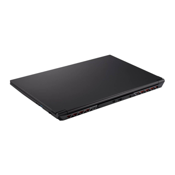
Introduction External Locator - Front & Right Side Views Figure 2 Front View 1. LED Indicators FRONT VIEW Figure 3 Right Side View 1. Speaker 2. Multi-in-1 Card Reader 3. USB 3.2 Gen 2 RIGHT SIDE VIEW Type-C Port 4. USB 3.2 Gen 1 Type-A Port 5. -
Page 18: External Locator - Left Side & Rear View
Introduction External Locator - Left Side & Rear View Figure 4 Left Side View 1. Security Lock Slot 2. Vent 3. USB 3.2 Gen 1 LEFT SIDE VIEW Type-A Ports 4. USB 2.0 Port 5. Microphone-In Jack 6. 2-In-1 Audio Jack (Headphone and Microphone) 7. -
Page 19: External Locator - Bottom View
Introduction External Locator - Bottom View Figure 6 Bottom View 1. Vent 2. RJ-45 LAN Jack 3. Speakers Overheating To prevent your com- puter from overhea- ting, make sure no- thing blocks any vent while the computer is in use. External Locator - Bottom View 1 - 7... -
Page 20: Mainboard Overview - Top (Key Parts)
Introduction Mainboard Overview - Top (Key Parts) Figure 7 Mainboard Top Key Parts 1 - 8 Mainboard Overview - Top (Key Parts) -
Page 21: Mainboard Overview - Bottom (Key Parts)
Introduction Mainboard Overview - Bottom (Key Parts) Figure 8 Mainboard Bottom Key Parts 1. Mini-Card Connector (M.2 SSD Module) 2. Mini-Card Connector (WLAN Module) 3. PCH 4. GPU 5. CPU 6. Memory Slots DDR4 SO-DIMM 7. KBC-ITE IT5570 Mainboard Overview - Bottom (Key Parts) 1 - 9... -
Page 22: Mainboard Overview - Top (Connectors)
Introduction Mainboard Overview - Top (Connectors) Figure 9 Mainboard Top Connectors 1. DC-In Jack 2. HDMI Port 3. Mini Display Port 4. Keyboard Cable Connector 5. LED KB Connector 6. USB 3.2 Gen 2 Type-C Port 7. USB 3.2 Gen 1 Type-A Port 8. -
Page 23: Mainboard Overview - Bottom (Connectors)
Introduction Mainboard Overview - Bottom (Connectors) Figure 10 Mainboard Bottom Connectors 1. Multi-in-1 Card Reader 2. LED Connector 3. Clickpad Cable Connector 4. HDD Cable Connector 5. CMOS Battery Connector 6. Audio Connector 7. Battery Connector 8. LCD Connector Mainboard Overview - Bottom (Connectors) 1 - 11... - Page 24 Introduction 1 - 12...
-
Page 25: Disassembly
Chapter 2: Disassembly Overview This chapter provides step-by-step instructions for disassembling the NP70HH / NP70HJ / NP70HK series notebook’s parts and subsystems. When it comes to reassembly, reverse the procedures (unless otherwise indicated). We suggest you completely review any procedure before you take the computer apart. -
Page 26: Maintenance Tools
Disassembly NOTE: All disassembly procedures assume that the system is turned OFF, and disconnected from any power supply (the battery is removed too). Maintenance Tools The following tools are recommended when working on the notebook PC: • M3 Philips-head screwdriver •... -
Page 27: Maintenance Precautions
Disassembly Maintenance Precautions The following precautions are a reminder. To avoid personal injury or damage to the computer while performing a re- moval and/or replacement job, take the following precautions: Power Safety Don't drop it. Perform your repairs and/or upgrades on a stable surface. If the computer falls, the case and other components Warning could be damaged. -
Page 28: Disassembly Steps
Disassembly Disassembly Steps The following table lists the disassembly steps, and on which page to find the related information. PLEASE PERFORM THE DISASSEMBLY STEPS IN THE ORDER INDICATED. To remove the Battery: 1. Remove the battery page 2 - 5 To remove the Keyboard: 1. -
Page 29: Removing The Battery
Disassembly Removing the Battery Figure 1 Battery Removal 1. Turn off the computer, turn it over. 2. Remove screws from the bottom case (Figure 1a). a. Remove the screws. 3. Carefully lift the bottom case up in the direction of the arrow at point and remove it (Figure 1b b. - Page 30 Disassembly 4. The battery will be visible at point on the computer (Figure 2c Figure 2 5. Carefully disconnect the cable , then remove screws (Figure 2d Battery Removal 6. Lift the battery off the computer (Figure 2e (cont’d.) 7. Reverse the process to install a new battery (do not forget to replace all the screws and the bottom cover). c.
-
Page 31: Removing The Keyboard
Disassembly Removing the Keyboard Figure 3 Keyboard Removal 1. Turn off the computer, turn it over and remove the battery (page 2 - 2. Remove screws from the bottom of the computer. a. Remove the screws from 3. Open it up with the LCD on a flat surface before pressing at point to release the keyboard module (use the spe- the bottom of the compu- cial eject stick... -
Page 32: Removing The Hard Disk Drive
Disassembly Removing the Hard Disk Drive Figure 4 HDD Assembly The hard disk drive can be taken out to accommodate other 2.5" serial (SATA) hard disk drives with a height of 7mm Removal (h). Follow your operating system’s installation instructions, and install all necessary drivers and utilities (as outlined in Chapter 4 of the User’s Manual) when setting up a new hard disk. - Page 33 Disassembly 4. Carefully lift and slightly slide the hard disk up Figure 5 5. Disconnect the hard disk assembly from the connector (Figure 5c HDD Assembly 6. Remove screws and bracket from the hard disk (Figure 5d Removal (cont’d.) 7. Reverse the process to install a new hard disk (do not forget to replace the screws). c.
-
Page 34: Removing The M.2 Ssd Module
Disassembly Removing the M.2 SSD Module Figure 6 M.2 SSD-1 Module M.2 SSD-1 Removal Procedure Removal 1. Turn off the computer, turn it over, remove the battery (page 2 - 2. The M.2 SSD module will be visible at point on the mainboard (Figure 6a). - Page 35 Disassembly M.2 SSD-2 Removal Procedure Figure 7 1. Turn off the computer, turn it over, remove the battery (page 2 - M.2 SSD-2 Module 2. The M.2 SSD module will be visible at point on the mainboard (Figure 7a). Removal 3.
- Page 36 Disassembly M.2 SSD-2 Installation Procedure Figure 8 M.2 SSD-2 Module 1. Turn off the computer, turn it over, remove the battery (page 2 - 5) and hard disk (page 2 - Installation 2. Disconnect the HDD connector cable (remove the screw and HDD bracket , if available) (Figure...
-
Page 37: Removing The System Memory (Ram)
Disassembly Removing the System Memory (RAM) Figure 9 RAM Module The computer has four memory sockets for 260 pin Small Outline Dual In-line Memory Modules (SO-DIMM) support- Removal ing DDR4 Up to 3200 MHz. The main memory can be expanded up to 32GB. The total memory size is automatically detected by the POST routine once you turn on your computer. -
Page 38: Removing The Wireless Lan Module
Disassembly Removing the Wireless LAN Module Figure 10 Wireless LAN 1. Turn off the computer, turn it over, remove the battery (page 2 - Module Removal 2. The Wireless LAN module will be visible at point on the mainboard (Figure 10a). -
Page 39: Wireless Lan, Combo Module Cables
Disassembly Wireless LAN, Combo Module Cables Note that the cables for connecting to the antennae on WLAN, WLAN & Bluetooth Combo, and LTE modules are not labelled. The cables/covers (each cable will have either a black or transparent cable cover) are color coded for identifi- cation as outlined in the table below. - Page 40 Disassembly 2 - 16...
-
Page 41: Part Lists
Appendix A: Part Lists This appendix breaks down the NP70HH / NP70HJ / NP70HK series notebook’s construction into a series of illustra- tions. The component part numbers are indicated in the tables opposite the drawings. Note: This section indicates the manufacturer’s part numbers. Your organization may use a different system, so be sure to cross-check any relevant documentation. -
Page 42: Part List Illustration Location
Part List Illustration Location The following table indicates where to find the appropriate part list illustration. Table A - 1 Part List Illustration Part Location page A - 3 page A - 4 Bottom page A - 5 Main Board page A - 6 page A - 7 A - 2... -
Page 43: Top
Figure A - 1 Top A - 3... -
Page 44: Bottom
Bottom Figure A - 2 Bottom A - 4 Bottom... -
Page 45: Main Board
Main Board Figure A - 3 Main Board Main Board A - 5... -
Page 46: Hdd
Figure A - 4 A - 6 HDD... -
Page 47: Lcd
Figure A - 5 LCD A - 7... - Page 48 A - 8...
-
Page 49: Schematic Diagrams
Schematic Diagrams Appendix B: Schematic Diagrams This appendix has circuit diagrams of the NP70HH / NP70HJ / NP70HK notebook’s PCB’s. The following table indi- cates where to find the appropriate schematic diagram. Diagram - Page Diagram - Page Diagram - Page... -
Page 50: System Block Diagram
Schematic Diagrams System Block Diagram NPX0HJ System Block Diagram (Tiger lake H) VDD3,VDD5 SHEET 42 nVIDIA 60W~80W GPU NVVDD PCI Express* GN20-P0/P1(NPx0HJ/HK) TIGER LAKE SHEET 53,54 (8x) N18P(NPx0HH) TGL-H 45W 5V,3.3V,5VS,3.3VS SHEET 10,11,12, 29x29mm eDP PANEL SHEET 44 DDIA (4x) 13,14,15,16,17,18 Connector 1358 Ball FCBGA... -
Page 51: Processor 1/6
Schematic Diagrams Processor 1/6 U20C 3 OF 15 PCIE4_RX_P_3 PCIE4_TX_P_3 PCIE4_RX_N_3 PCIE4_TX_N_3 PCIE4_RX_P_2 PCIE4_TX_P_2 PCIE4_RX_N_2 PCIE4_TX_N_2 PCIE4_RX_P_1 PCIE4_TX_P_1 3.3V PCIE4_RX_N_1 PCIE4_TX_N_1 PCIE4_RX_P_0 PCIE4_TX_P_0 PCIE4_RX_N_0 PCIE4_TX_N_0 PCIE16_RX_P_15 PCIE16_TX_P_15 *h6_2b4_0d4_0 *h6_2b4_0d4_0 *h6_2b4_0d4_0 PCIE16_RX_N_15 PCIE16_TX_N_15 PCIE16_RX_P_14 PCIE16_TX_P_14 EWTF02-104F4F-N PCIE16_RX_N_14 PCIE16_TX_N_14 PCIE16_RX_P_13 PCIE16_TX_P_13 PCIE16_RX_N_13 PCIE16_TX_N_13 THERM_VOLT 40 PCIE16_RX_P_12... -
Page 52: Processor 2/6
Schematic Diagrams Processor 2/6 U20A M_A_DQ[63:0] U20B DDR4(IL) / DDR4(NIL) DDR4 M_B_DQ[63:0] M_A_DQ63 1 OF 15 DDR4(IL) / DDR4(NIL) DDR4 M_A_DQ62 DDR0_DQ7_7/DDR1_DQ5_7 DDR0_CLK_P3 M_B_DQ63 2 OF 15 M_A_DQ61 DDR0_DQ7_6/DDR1_DQ5_6 DDR0_CLK_N3 M_B_DQ62 DDR1_DQ7_7/DDR1_DQ7_7 DDR1_CLK_P3 M_A_DQ60 DDR0_DQ7_5/DDR1_DQ5_5 DDR0_CLK_P2 M_B_DQ61 DDR1_DQ7_6/DDR1_DQ7_6 DDR1_CLK_N3 DDR0_DQ7_4/DDR1_DQ5_4 DDR0_CLK_N2 DDR1_DQ7_5/DDR1_DQ7_5 DDR1_CLK_P2... -
Page 53: Processor 3/6
Schematic Diagrams Processor 3/6 U20E CLKOUT_CPUBCLK_DP H_PRDY# 100_04 CLKOUT_CPUBCLK_DN CLKOUT_CPUBCLK_DP CPU_ID_R CPU_ID VCCIO 5 OF 15 R537 0_04 CLKOUT_CPU_PCI_BCLK_DP BCLK_P RSVD_18 CLKOUT_CPUBCLK_DN CPU_ID R538 10K_04 CLKOUT_CPU_PCI_BCLK_DN BCLK 3.3VA CFG_15 CLKOUT_CPU_PCI_BCLK_DP CFG_15 CFG_14 100_1%_04 VCCST CLKOUT_CPU_PCI_BCLK_DN PCI_BCLK_P CFG_14 CFG_13 H_SKTOCC_N R453 56.2_1%_04 R547 100K_04... -
Page 54: Processor 4/6
Schematic Diagrams Processor 4/6 VCCIN VCCIN VCCIN VCCIN U20J U20K 10 OF 15 11 OF 15 AB11 CB30 CG16 CN30 VCCIN_140 VCCIN_215 VCCIN_1 VCCIN_73 AC11 CB31 CG17 CN31 VCCIN_141 VCCIN_216 VCCIN_2 VCCIN_74 AC12 CB33 CG18 CN33 VCCIN_142 VCCIN_217 VCCIN_3 VCCIN_75 AD11 CB34 CG20... -
Page 55: Processor 5/6
Schematic Diagrams Processor 5/6 VDDQ U20N VCCIN_AUX VCCIO U20L 14 OF 15 AH11 VSS_572 VDD2_1 AA34 12 OF 15 VCCST AH12 VCCIN_AUX_1 VCCIO_OUT VSS_573 VDD2_2 AA36 AJ11 VCCIN_AUX_2 VSS_574 VDD2_3 VCCIN_AUX VCCIN_AUX AA39 AJ12 VCCIN_AUX_3 VCCST_1 VSS_575 VDD2_4 AB33 AL11 VCCIN_AUX_4 VCCST_2 VSS_576... -
Page 56: Processor 6/6
Schematic Diagrams Processor 6/6 U20F U20G U20H U20I 7 OF 15 6 OF 15 8 OF 15 9 OF 15 BN36 CB39 CU27 VSS_412 VSS_492 VSS_252 VSS_332 VSS_92 VSS_172 VSS_1 VSS_46 AL10 BA36 BN39 CC10 VSS_413 VSS_493 VSS_253 VSS_333 VSS_93 VSS_173 VSS_2 VSS_47... -
Page 57: Ddr4 Cha So-Dimm_0
Schematic Diagrams DDR4 CHA SO-DIMM_0 Channel A SO-DIMM 0[RAM1] VTT_MEM VDDQ J_DIMMA_1B 2.5V J_DIMMA_1A M_A_DQ[63:0] 3 VDD19 VDD18 M_A_DQ0 M_A_CLK_DDR0 CK0_T M_A_DQ2 VDD17 M_A_CLK_DDR#0 CK0_C VDD16 VPP2 M_A_DQ4 M_A_CLK_DDR1 CK1_T VDD15 VPP1 M_A_DQ5 M_A_CLK_DDR#1 CK1_C VDD14 M_A_DQ1 M_A_DQ3 VDD13 3.3VS M_A_CKE0 CKE0 M_A_DQ7... -
Page 58: Ddr4 Chb So-Dimm_0
Schematic Diagrams DDR4 CHB SO-DIMM_0 VTT_MEM J_DIMMB_1B Channel B SO-DIMM 0[RAM2] VDDQ 2.5V VDD19 VDD18 VDD17 J_DIMMB_1A VDD16 VPP2 M_B_DQ[63:0] 3 VDD15 VPP1 M_B_DQ4 M_B_CLK_DDR0 CK0_T VDD14 DDR4_DRAMRST# M_B_DQ3 8,27 DDR4_DRAMRST# M_B_CLK_DDR#0 CK0_C M_B_DQ5 VDD13 3.3VS M_B_CLK_DDR1 CK1_T VDD12 M_B_DQ7 M_B_CLK_DDR#1 CK1_C VDD11... -
Page 59: Vga Pci Express
Schematic Diagrams VGA PCI Express NV PCI EXPRESS 1V8_AON R508 0_04 20,53 NVVDD_PWRGD R512 *0_04 DGPU_PWRGD R515 10K_04 2SK3018S3 GFX_CLKREQ0# U19A GN20/QN20-P R514 BGA1358 1V8_AON COMMON R712 *10K_04 *10K_04 1V8_AON 1/17 PCI_EXPRESS PEX_VDD R713 *10K_04 *2SK3018S3 AP11 C125 C150 C137 C622 PEX_WAKE PEX_WAKE#... -
Page 60: Gpu Frame Buffer Partition
Schematic Diagrams GPU Frame Buffer Partition U19B U19C 2/17 FBA 3/17 FBB FBA_D[31..0] FBB_D[31..0] FBA_D[31..0] FBB_D[31..0] FBA_D0 1V8_FB_PLL_REF FBB_D0 FBA_D0 FB_PLLVDD 1V8_FB_PLL_REF FBB_D0 FBA_D1 FBB_D1 C146 FBA_D1 FBB_D1 FBA_D2 FBB_D2 FBA_D2 1u_6.3V_X6S_04 FBB_D2 FBA_D3 FBB_D3 FBA_D3 FBB_D3 FBVDDQ FBA_D4 FBB_D4 FBA_D4 FBB_D4 FBA_D5... - Page 61 Schematic Diagrams Frame Buffer A FRAME BUFFER PARTITION B 31..0 FBA_DBI[3..0] FBA_DBI[3..0] FBA_DBI0 FBA_DBI1 FBA_DBI2 FBA_DBI3 FBA_CMD[24..0] FBA_CMD[24..0] FBVDDQ FBA_EDC[3..0] FBA_EDC[3..0] FBA_EDC0 FBA_EDC1 FBA_EDC2 FBA_EDC3 FBA_D[31..0] FBA_D[31..0] FBA_CMD1 FBA_VREFC CA0_A VREFC FBA_CMD13 CA1_A FBA_CMD12 CA2_A FBA_CMD24 CA3_A R445 FBA_CMD11 CA4_A FBA_CMD15 1K_1%_04 CA5_A...
-
Page 62: Frame Buffer A
Schematic Diagrams Frame Buffer A FRAME BUFFER PARTITION A 63..32 M10D FBA_DBI[7..4] COMMON FBA_DBI[7..4] FBVDDQ FBA_DBI4 FBA_DBI5 FBA_DBI6 M10C FBA_DBI7 COMMON FBA_EDC[7..4] FBA_CMD[52..28] FBA_EDC[7..4] FBA_CMD[52..28] FBA_EDC4 FBA_CMD33 FBA_VREFC_H CA0_A VREFC FBA_EDC5 FBA_CMD45 CA1_A FBA_EDC6 FBA_CMD35 CA2_A FBA_EDC7 FBA_CMD46 CA3_A FBA_CMD36 R440 CA4_A FBA_D[63..32]... - Page 63 Schematic Diagrams Frame Buffer B FRAME BUFFER PARTITION B 31..0 FBB_DBI[3..0] FBB_DBI[3..0] FBB_DBI0 FBB_DBI1 FBB_DBI2 M11D FBB_DBI3 FBB_EDC[3..0] FBVDDQ FBB_EDC[3..0] FBB_CMD[24..0] FBB_EDC0 FBB_CMD[24..0] FBB_EDC1 FBB_EDC2 FBB_EDC3 M11C FBB_D[31..0] FBB_CMD1 FBB_VREFC CA0_A VREFC FBB_D[31..0] FBB_CMD13 CA1_A FBB_CMD12 CA2_A FBB_CMD24 CA3_A FBB_CMD11 CA4_A M11A FBB_CMD15...
-
Page 64: Frame Buffer B
Schematic Diagrams Frame Buffer B FBB_DBI[7..4] FRAME BUFFER PARTITION B 63..32 FBB_DBI[7..4] FBB_DBI4 FBB_DBI5 FBB_DBI6 FBB_DBI7 FBB_EDC[7..4] FBB_EDC[7..4] M12D FBB_EDC4 FBB_EDC5 FBB_CMD[52..28] FBB_EDC6 FBB_CMD[52..28] FBVDDQ FBB_EDC7 FBB_D[63..32] FBB_D[63..32] M12C FBB_CMD33 FBB_VREFC_H CA0_A VREFC FBB_CMD45 M12A M12B CA1_A FBB_CMD35 CA2_A FBB_CMD46 CA3_A FBB_CMD36 R456... -
Page 65: Vga Nvvdd Coupling
Schematic Diagrams VGA NVVDD Coupling FBVDDQ NVVDD C238 C237 C309 C342 C343 C344 C341 C318 C256 C136 C148 C133 C222 C130 C131 C122 C147 C155 C174 C141 C173 Sheet 16 of 62 VGA NVVDD Coupling C152 C190 C188 C194 C264 C161 C162 C163... -
Page 66: Straps And Xtal
Schematic Diagrams Straps and XTAL XTAL U19Q GPU_PLLVDD 1V8_RUN 11/17 XTAL_PLL 40mil GPU_PLLVDD HCB1608KF-300T60 CORE_PLL_AVDD GPCADC_AVDD 1V8_AON C275 C268 C258 C257 SP_PLLVDD C316 C283 1u_6.3V_X6S_04 1u_6.3V_X6S_04 1u_6.3V_X6S_04 1u_6.3V_X6S_04 AJ10 VID_PLLVDD 22u_6.3V_X6S_08 4.7u_6.3V_X6S_06 R554 *100K_1%_04 XTALOUTBUFF XTALSSIN EXT_REFCLK_FL XTAL_OUTBUFF MULTI-LEVEL STRAPS XTAL_IN XTAL_OUT R553... -
Page 67: Ifp I/O Interface
Schematic Diagrams IFP I/O Interface DP to TYPE-C IFP I/O INTERFACE U19L 5/17 IFPAB HDMI U19M SL/DL 6/17 IFPC HDMI IFPA_L3 TXC/TXC R517 1K_1%_04 TXC/TXC IFPA_L3 IFPCD_RSET R516 1K_1%_04 IFPAB_RSET HDMI IFPA_L2 TXD0/0 IFPA_L2 IFPC_AUX_SDA TXD0/0 IFPC_AUX_SCL IF_PLLVDD IFPAB_PLLVDD IFPA_L1 TXD1/1 40 mil C307... -
Page 68: Misc - Gpio, I2C And Vbios
Schematic Diagrams Misc - GPIO, I2C and VBIOS MISC: GPIO, I2C, and ROM N18P GN20P U19P NV3V3 1V8_AON R585 10K_04 12/17 MISC2 1V8_AON NV3V3 R581 10K_04 R585 10K_04 R608 R607 VGA_ROM_CS# 1V8_AON 0_04 *10K_04 ROM_CS VBIOS ROM 1M VGA_ROM_SI GPIO26_ROM_WP# R624 R606 ROM_SI... -
Page 69: Nvidia Power Sequence
Schematic Diagrams NVIDIA Power Sequence DEFAULT HW POWER SEQUENCE 3.3VS R635 3.3VA 100K_04 BAT54AS3 FBVDDQ_PWRGD 56 FBVDDQ_EN NV_FBVDDQ_EN 56 10,20 DGPU_PWRGD PEX_VDD_PWRGD 55 NV_EN_DOWN VIN_DOW N PEX_VDD_EN NV_PEXVDD_EN 55 NV_NVVDDS_EN R707 0_04 OVERT# OVERT#_EC 40 OVERT# NVVDDS_EN 1V8_AON_PWRGD SUSB# NVVDD_EN NV_NVVDD_EN 53,54 R702 0_04... -
Page 70: Gpu Nvvdd, Fbvddq
Schematic Diagrams GPU NVVDD, FBVDDQ NVVDD U19J NVVDD FBVDDQ FBVDDQ 14/17 FBVDDQ U19G U19H NVVDD NVVDD AA31 FBVDDQ FBVDDQ AA36 4/17 VDDMS 13/17 VDD FBVDDQ FBVDDQ AB33 FBVDDQ FBVDDQ AA12 AJ22 AA13 AB34 VDDMS VDDMS FBVDDQ FBVDDQ AA29 AJ23 AA14 AB35 VDDMS VDDMS... -
Page 71: Gpu Gnd
Schematic Diagrams GPU GND GPU GND U19D U19E 15/17 GND_1/2 16/17 GND_2/2 AN10 AN31 AN33 AN34 AN35 AN39 AP12 U19F AP14 NVVDD NVVDD AB13 AP16 9/17 Configurable AB14 AP18 Power Channels AB15 AB16 AP20 XVDD XVDD AB17 AP32 XVDD XVDD AB18 AP37 XVDD... -
Page 72: Mdp
Schematic Diagrams NV_MDP_PW R 3.3V VOUT C557 C556 10u_6.3V_X5R_06 *10u_6.3V_X5R_06 SY6288D20AAC NV_MDP_PW R SYT16B05DVD 38,44,45 SUSB I_MDP_D3 I_MDP_D3J GND1 COMMON I_MDP_D#3 I_MDP_D#3J GND2 I_MDP_AUX_R I_MDP_AUX_J I_MDP_AUX#_R I_MDP_AUX#_J I_MDP_AUX#_J AUX_CHN I_MDP_D#2J I_MDP_AUX_J LANE_2N AUX_CHP I_MDP_D#0 I_MDP_D2J 0.1u_10V_X5R_04 LANE_2P DP_E#0 I_MDP_D0 *DVI2012F2SF-900T05_08-SHORT 0.1u_10V_X5R_04 DP_E0 I_MDP_D#3J... -
Page 73: Panel,Inverter
Schematic Diagrams Panel, Inverter PANEL POWER DEFAULT PANEL CONNECTOR SHORT VLED PJ21 OPEN_2A LED PANEL (EDP Channel). PLVDD J_LCD1 *MTP3403N3 C187 C608 C607 D02A 1u_6.3V_X5R_02 EMC2 1000p_50V_X7R_04 3.3V C176 0.1u_10V_X5R_04 *0.22u_25V_X7R_06 EDP_TXN_0 C166 0.1u_10V_X5R_04 *4.7K_06 EDP_TXP_0 C154 0.1u_10V_X5R_04 GND5 *150K_04 EDP_TXN_1 GND5 GND4... -
Page 74: Hdmi
Schematic Diagrams HDMI TMDS_CLOCK#_R TMDS_CLOCK#J TMDS_CLOCK_R TMDS_CLOCKJ TMDS_DATA0#_R TMDS_DATA0#J EMR8 0_1%_02 TMDS_DATA0_R TMDS_DATA0J EMR7 0_1%_02 HDMI CONNECTOR SYT16B05DVD HDMI_5VS TMDS_DATA1#_R TMDS_DATA1#J EMR6 0_1%_02 J_HDMI1 TMDS_DATA1_R TMDS_DATA1J EMR5 0_1%_02 VOUT TMDS_DATA2#_R TMDS_DATA2#J C582 C579 C587 EMR4 0_1%_02 TMDS_DATA2_R TMDS_DATA2J EMR3 0_1%_02 HDMI_HPD-C-R HOT PLUG DETECT APL3517A... -
Page 75: Pch 1/7
Schematic Diagrams PCH 1/7 U37F XTAL38.4_OUT XTAL38.4_OUT 6 OF 9 12p_50V_NPO_04 C727 XTAL_OUT USB31_4_TXP USB3_TXP4 35 XTAL38.4_IN XTAL38.4_IN XTAL_IN USB31_4_TXN USB3_TXN4 35 USB31_4_RXP USB3_RXP4 35 R632 60.4_1%_04 USB3_RXN4 35 XCLK_BIASREF USB31_4_RXN R633 AC17 USB3_TXP3 35 RSVD_1 USB31_3_TXP 200K_1%_04 AC15 RSVD_2 USB31_3_TXN USB3_TXN3 35 XTAL19001-X-022-3... -
Page 76: Pch 2/7
Schematic Diagrams PCH 2/7 U37B TGP_H_IP_EXT GPD_12 2 OF 9 R337 0_04 AL47 GPD12 DMI7_TXP DMI_IT_MR_7_DP LAN_DISABLE_N AK46 DMI_IT_MR_7_DN SLP_S5# GPD11/LANPHYPC DMI7_TXN LAN_WAKEUP# T101 R811 *10K_04 AJ47 PCH_SLP_WLAN# GPD10/SLP_S5# DMI7_RXP DMI_MT_IR_7_DP VDD3 AJ46 SUS_CLK_R GPD9/SLP_WLAN# DMI7_RXN DMI_MT_IR_7_DN SUS_CLK R335 33_04 R336 *1K_04 AJ45... - Page 77 Schematic Diagrams PCH 3/7 3.3VS C449 *27P_25V_NPO_02 LAN_CLKREQ# U37C PEG_CLKREQ# 10K_8P4R_04 CARD_CLKREQ# 3 OF 9 R259 *33_04 AU21 AY12 DMIC_DATA0 GPP_S7/SNDW4_DATA/DMIC_DATA0 GPP_H23/TIME_SYNC0 GPP_H23_SSD1_RST# 34 SSD_CLKREQ# R252 *33_04 I2C1_SCL AW21 BD10 DMIC_CLK0 GPP_S6/SNDW4_CLK/DMIC_CLKA0 GPP_H22/ISH_I2C1_SCL I2C1_SDA AY20 BE10 GPP_S5/SNDW3_DATA/DMIC_DATA1 GPP_H21/ISH_I2C1_SDA DGPU_PWR_EN *10K_04 R820 BB20 GPP_S4/SNDW3_CLK/DMIC_CLKA1...
- Page 78 Schematic Diagrams PCH 4/7 U37D 4 OF 9 PM_CLKRUN# AU29 AW46 PM_CLKRUN# GPP_D23/UART3_CTS#/THC1_SPI2_INT# GPP_A14/IMGCLKOUT0 AY30 AV46 UART2_TXD GPP_D22/UART3_RTS#/THC1_SPI2_RST# GPP_A13/ESPI_ALERT3# R281 *0_06 AW29 AV47 UART2_RXD GPP_D21/UART3_TXD/THC1_SPI2_IO3 GPP_A12/ESPI_ALERT2# LAN_WUP1# R269 *0_06 BD30 AU45 *0_04 R772 LAN_WAKEUP# 27,34,37,40 GPP_D20/UART3_RXD/THC1_SPI2_IO2 GPP_A11/ESPI_ALERT1# BD35 AU46 SERIRQ_ESPI_ALERT0 SMB_DATA 52 GPP_D19/GSPI3_MOSI/THC1_SPI2_IO1 GPP_A10/ESPI_ALERT0#...
- Page 79 Schematic Diagrams PCH 5/7 U37A 1 OF 9 CPU_C10_WAKE C10_WAKE CLKOUT_PCIE_P15 CLKOUT_PCIE_N15 CLKOUT_CPUBCLK_DP CLKOUT_CPUBCLK_DP CLKOUT_CPUBCLK_P CLKOUT_CPUBCLK_DN CLKOUT_CPUBCLK_DN CLKOUT_CPUBCLK_N CLKOUT_PCIE_P14 CLKOUT_PCIE_N14 CLKOUT_CPUNSSC_DP CLKOUT_CPUNSSC_DP CLKOUT_CPUNSSC_P CLKOUT_CPUNSSC_DN CLKOUT_CPUNSSC_DN CLKOUT_CPUNSSC_N CLKOUT_PCIE_P13 CLKOUT_PCIE_N13 CLKOUT_CPU_PCI_BCLK_DP CLKOUT_CPU_PCI_BCLK_DP CLKOUT_CPUPCIBCLK_P CLKOUT_CPU_PCI_BCLK_DN CLKOUT_CPU_PCI_BCLK_DN CLKOUT_CPUPCIBCLK_N CLKOUT_PCIE_P12 CLKOUT_PCIE_N12 CLKOUT_CPURTC CLKOUT_CPURTC CLKOUT_PCIE_P11 CLKOUT_CPUBCLK2_P AC11 CLKOUT_CPUBCLK2_P CLKOUT_PCIE_N11...
-
Page 80: Pch 6/7
Schematic Diagrams PCH 6/7 VCCLDOSTD_OUT_0P85 VCC_RTC 1.8VA U37G 3.3VA 7 OF 9 VCCST_OVERRIDE VCCST_OVERRIDE VCCST_OVERRIDE VCCLDOSTD_0P85_1 VCCLDOSTD_0P85_2 C389 C492 C491 C458 C431 VCCPRIM_3P3_1 VCCLDOSTD_0P85_3 2.2u_6.3V_X5R_04 VCC_RTC BF46 AA38 VCCRTC_1 VCCIN_AUX_1 VCCPRIM_1P05 BG46 AC38 VCCRTC_2 VCCIN_AUX_2 372uA BG47 AC39 VCCRTC_3 VCCIN_AUX_3 VCCPRIM_1P05 AC41 VCCIN_AUX_4... -
Page 81: Pch 7/7
Schematic Diagrams PCH 7/7 U37H U37I 8 OF 9 9 OF 9 AJ23 AW25 VSS_163 VSS_240 VSS_1 VSS_78 AJ25 AW39 VSS_164 VSS_241 VSS_2 VSS_79 AJ27 AY25 VSS_165 VSS_242 VSS_3 VSS_80 *M-MARK *M-MARK *M-MARK AJ28 AY43 VSS_166 VSS_243 VSS_4 VSS_81 AK12 VSS_167 VSS_244 VSS_5... -
Page 82: Audio Codec
Schematic Diagrams Audio Codec HEADPHONE_R HEADPHONE_L AUDIO CODEC ALC256 LINE1-VREFO-L LINE1-VREFO-R MIC2-VREFO AUDG C534 10u_6.3V_X5R_06 AUDG 50271-0020N-001 SPKOUTR+_R R417 100K_04 SPKOUTR+ ANALOG DIGITAL 5VS_AUD HCB1005KF-121T20 HCB1608KF-800T30 C518 J_SPKR1 C514 180p_50V_NPO_04 *1u_6.3V_X5R_02 C837 C526 C520 SPKOUTR-_R SPKOUTR- HCB1608KF-800T30 C517 1.8VS AUDG 180p_50V_NPO_04 SPKOUTL+_L SPKOUTL+... -
Page 83: Wlan+Bt, Pcie 4X Ssd
Schematic Diagrams M.2 WLAN+BT, PCIE 4X SSD WLAN+BT VDD3 R699 0_04 26,36,37 PCIE_WAKE# WLAN_3.3V J_WLAN1 WLAN_WAKE_N R703 *0_04 40 mil 27,29,37,40 LAN_WAKEUP# >120 mil >120 mil WLAN_3.3V GND13 3.3V3 CNVI_WT_CLKP WT_CLKP 3.3V2 VOUT C459 C453 CNVI_WT_CLKN WT_CLKN PEWAKE1_N R678 *0_04 C404 WLAN_CLKREQ_3# WLAN_CLKREQ#... -
Page 84: Type-C & A
Schematic Diagrams Type-C & A J_TYPEC1 UCF3T-21S01-0P11 USBVCC3.1_1 A_UTXP_SW2_J USB3_RXP4_J 100 MIL A_UTXN_SW2_J TX0_P RX0_P USB3_RXN4_J C699 USB3.1 PORT(PORT1) W/O USB CHARGER TX0_N RX0_N VDD5 USBVCC_CH 10u_6.3V_X5R_06 C710 C712 USBVCC3.1_1 VBUS VBUS USBVCC3.1_1 80 mil TYPEC_CC1 *0.1u_6.3V_X5R_02 0.1u_6.3V_X5R_02 80 mil SBU2 TYPEC_UDP_J TYPEC_UDN_J... -
Page 85: Card Reader Rts5227S Rtd3
Schematic Diagrams Card Reader RTS5227S RTD3 RTS5227S OZ711LV2 VDD3 J_CARD-REV1 3V3AUX 3.3VS SD_D3 3V3AUX CD/DAT3 SD_WP# VCC_CARD SD_CMD CR1_LEDN R241 10K_04 40 mil VSS1 SD_CD# R240 R698 MS_INS# SD_CLK 0_04 *10K_04 C485 C480 C476 VSS2 SD_D0 C751 C752 DAT0 SD_D1 26,34,37 PCIE_WAKE# SD_D2... -
Page 86: Lan Rtl8111H Rtd3
Schematic Diagrams LAN RTL8111H RTD3 LAN (RTL8111H LDO MODE ONLY) (W>60mil VDD10 L<200mil) REGOUT R653 *28mil short-p (>60mil) C383 C364 C385 3.3V_AUX VDD3 R169 2.49K_1%_04 0.1u_6.3V_X5R_02 *4.7u_6.3V_X5R_06 *0.1u_6.3V_X5R_02 R651 *28mil short-p LED0 LED1/GPO RTL8111H LED2 R850 0_04 XTAL2 GCLK_25M_GLAN R643 10K_04 AVDD33 R642... -
Page 87: Hdd, Click Tp, Audio
Schematic Diagrams HDD, Click TP, Audio FOR SUPPORT OPTANE project, SATA HDD POWER GATEING HDD CONNECT1 (MASTER) J_HDD1 JHDD_SATA_TXP3 C817 0.01u_16V_X7R_04 SATA_TXP3 27 JHDD_SATA_TXN3 DEFAULT C813 0.01u_16V_X7R_04 SATA_TXN3 27 SHORT SATA_5VS JHDD_SATA_RXN3 C819 0.01u_16V_X7R_04 SATA_RXN3 27 JHDD_SATA_RXP3 C830 0.01u_16V_X7R_04 SATA_RXP3 27 PJ14 OPEN-3mm SATA_5VS... -
Page 88: Led, Ccd, Tpm, Power Sw Bd
Schematic Diagrams LED, CCD, TPM, Power SW Bd. VDD_TPM R373 *0_04 3.3VA R422 0_04 VDD3 R389 R400 *4.7K_04 4.7K_04 TPM_GPIO GPIO0 TPM_PP VDD_TPM R378 4.7K_04 C540 C834 C513 C839 20,29,34,36,37,40 BUF_PLT_RST# RST# VSS_3 0.1u_6.3V_X5R_02 0.1u_6.3V_X5R_02 1u_6.3V_X5R_02 0.1u_6.3V_X5R_02 TPM_PIRQ# PIRQ# NC_1 NC_2 R414 56_1%_04... -
Page 89: Kbc-Ite It5570
Schematic Diagrams KBC-ITE IT5570 EC ROM Debug Port C460 VDD3 IT5570 *0.1u_6.3V_X5R_02 KBC_AVDD HCB1005KF-121T20 VDD3 ALSPI_MSI_L R262 33_04 VDD3 J_80DEBUG1 ALSPI_MSO_L C758 R266 33_04 R255 3IN1 3.3K_1%_04 34,40 3IN1 ALSPI_CE#_L 0.1u_6.3V_X5R_02 80CLK R278 0_04 FDIO2 34,40 80CLK ALSPI_SCLK_L R273 33_04 R264 KBC_AGND 3.3K_1%_04... -
Page 90: Rgb Kb
Schematic Diagrams RGB KB RGB KB Only VDD3 RGBKB_PWR J_KBLED1 R260 *100K_04 RGB_SS 1K_04 R355 0_06 R279 RGBKBSW_R KBZONE_R RGBKB-DET_R 100_04 RGBKB-DET# 40 KBZONE_B R271 KBZONE_R KBZONE_G SM3422KTDSH EC_PWM_LEDKB_R FP225H-008S11M R353 0_06 RGBKBSW_G KBZONE_G RGBKB_PWR Sheet 41 of 62 SM3422KTDSH EC_PWM_LEDKB_G J_KBLED2 RGB KB... -
Page 91: Vdd3,Vdd5
Schematic Diagrams VDD3, VDD5 PR107 PR109 24K_1%_04 24K_1%_04 EN_3V EN_5V PJ35 *CV-40mil PC51 1000p_50V_X7R_04 2.5A VREG3 PC259 PC274 PC266 PC57 PC275 PC272 PC268 PC258 VDD3 PC68 1u_6.3V_X5R_04 VREG3 PGOOD PC58 PC59 VDD5 PR103 0_06 PR102 0_06 VBST2 VBST1 0.1u_10V_X7R_04 0.1u_10V_X7R_04 PR101 0_06 PR100... -
Page 92: 1V8_Run/Aon, Nv3V3, 3.3Va
Schematic Diagrams 1V8_RUN/AON, NV3V3, 3.3VA VREG5 1.8VA PU21 AOZ2261NQI-11 PR252 0_06 PC249 PC237 PC244 3.3VA PC254 4.7u_6.3V_X5R_04 PR244 180K_1%_04 PR246 PR257 0_06 PC265 0.1u_16V_X7R_04 10K_1%_04 1.8VA_PWRGD PGOOD 1.8VA_PWRGD PR242 *10K_1%_04 VREG5 PS_1V8_PFM 1.8VA PFM* PR239 PL20 10K_1%_04 BCIHP5420HC-1ROM PR245 10K_04 PJ30 *CV-40mil PC247... -
Page 93: 5V,3Vs,5Vs
Schematic Diagrams 3V, 5V, 3VS, 5VS VDD3 DD_ON# R655 VDD5 VDD5 300_1%_04 R756 C447 EM5209 C410 *100_04 0.1u_6.3V_X5R_02 R770 0.1u_6.3V_X5R_02 2SK3018S3 *2SK3018S3 10K_04 DD_ON# DD_ON# OUT1 OUT2 DD_ON# 35 SUSB OUT1 OUT2 C441 C413 2SK3018S3 0.1u_6.3V_X5R_02 DEFAULT SHORT 0.1u_6.3V_X5R_02 C423 C774 35,40,42,45 DD_ON... -
Page 94: V,1.8Vs,1.8Va_C10
Schematic Diagrams 1.8V, 1.8VS, 1.8VA, C10 1.8VA 1.8VA 1.8VS C759 1.8V C761 G5016 0.1u_6.3V_X5R_02 *0.1u_10V_X5R_04 1.8V 1.8VS OUT1 OUT2 OUT1 OUT2 C748 C757 DEFAULT SHORT R700 *0.1u_10V_X5R_04 0.1u_6.3V_X5R_02 100_06 C750 C749 220p_50V_NPO_04 *220p_50V_NPO_04 2SK3018S3 VDD3 24,27,29,35,44,46,47,52 SUSB# SUSB 23,38,44 R744 *10K_04 35,40,42,44 DD_ON... -
Page 95: Vccst, Vccstg
Schematic Diagrams VCCST, VCCSTG 1.05V VCCST VCCSTG VCCST VCC1.05_OUT_FET VCC1.05_OUT_FET VCCSTG VOUT VOUT C623 C624 C618 C455 C457 C753 *10u_6.3V_X5R_06 1u_6.3V_X5R_02 0.1u_6.3V_X5R_02 *10u_6.3V_X5R_06 1u_6.3V_X5R_02 0.1u_6.3V_X5R_02 R452 VDD3 R674 VDD3 *33_04 *33_04 R451 R708 Q48A *100K_04 Q48B *100K_04 *MTDK3S6R *MTDK3S6R VDD3 VDD3 R722 PJ22... -
Page 96: Vnn / V1.05
Schematic Diagrams VNN / V1.05 PR233 V1.05A BYPASS RAIL 3.3_06 PR251 0_04 V1.05A_EN PR249 0_04 PC232 0.22u_10V_X5R_04 V1.05A_EXT_OUT VCC_V1P05EXT_1P05 PU20 PL18 CIHP-0420-1R0-M PJ29 PC48 PC47 PC49 PC235 PC234 PC239 PC238 PC271 *2mm 4.7u_25V_X5R_08 4.7u_25V_X5R_08 0.1u_25V_X7R_06 VOUT 3.3VA VCCIN_AUX_PG_R V1.05A_EN PR250 10K_04 NB695AGD-Z PC250... -
Page 97: Vccin
Schematic Diagrams VCCIN PR132 0_04 VCCIN_TEMP VCCIN_EN PR117 10K_04 PJ18 *CV-40mil 3.3V VDD3 PC77 *0.1u_16V_X7R_04 PR136 PC82 DEFAULT SHORT 49.9K_1%_04 1u_16V_X7R_06 PJ17 4,24,29,40 ALL_SYS_PW RGD PR123 VCCST 4.7_1%_06 PR139 0_04 PSYS PC86 *0.01u_50V_X7R_04 PC80 4.7u_6.3V_X6S_06 PR147 PR140 4.87K_1%_04 2M_1%_04 PR118 *1K_1%_04 VR_HOT_N PR121... -
Page 98: Vccin Output
Schematic Diagrams VCCIN Output phase 1 3.3V PC135 PC102 PC109 PC119 PU11 MP86941GQVT-Z 0.1u_25V_X7R_06 VIN1 PC127 VIN2 1u_6.3V_X6S_04 BST_PWM1 AGND VCCIN VCCIN_PWM1 PR168 0_04 PC139 1u_25V_X7R_06 SW_PWM1 PR172 0_04 48,49 VCCIN_TEMP VTEP/FLT CMME063T-R15MS0R907 48,49 VCCIN_SYNC SYNC PGND9 PGND8 PC152 PGND7 PR176 0_04 0.1u_16V_X7R_04... -
Page 99: Ac_In, Charger
Schematic Diagrams AC_In, Charger EML2 HCB2012KF-800T80 AC Detect 17.2V MDU1517 MDU1721 J_DC_JACK1 PRS1 2DC3003-016211F EML1 HCB2012KF-800T80 WMCSL0612R010FETA DC_19V ULTRASO-8 ULTRASO-8 PC15 PC12 PC14 PC123 PC121 PC122 PC124 PC108 PC87 PC106 PC88 PC112 PR12 4.7_06 4.7_06 PQ17 MDU1517 26786_PA PC171 *0.1u_25V_X7R_06 PC43 26786_VAD PC170... -
Page 100: Vccin Aux
Schematic Diagrams VCCIN AUX PR13 VCCIN_AUX 200_1%_04 330p_50V_NPO_04 PR188 PR11 *100_04 10K_1%_04 *20mil short-p VCCIN_AUX_VCCSENSE 5,31 PR20 *20mil short-p 330p_50V_NPO_04 VCCIN_AUX_VSSSENSE 5,31 PR17 PR187 14.3K_1%_04 *100_04 47p_50V_NPO_04 33.2K_1%_04 PC107 PR162 0.1u_16V_X7R_04 16.5K_1%_04 PR165 4.32K_1%_04 PC16 PC13 PC11 PR14 *20mil short-p AGND_P PR156 10K_04... -
Page 101: Ddr 1.2V/0.6Vs,2.5V
Schematic Diagrams DDR 1.2V / 0.6VS, 2.5V DDR4 1.2V/0.6VS PC256 PC263 PC267 RB0540S2 G5616BRZ1U VDDQ_R VTT_MEM(0.6V) PC61 PC55 SHORT VLDOIN VBST EMR2 10u_6.3V_X5R_06 0.1u_25V_X7R_06 VDDQ_R 1.2V SHORT VTT_MEM DRVH PJ16 PL19 0_06 TMPC0603H-1R0M-Z01 PC72 VTTGND VDDQ PR108 *15mil_short PC230 E-jump-6mm 22u_6.3V_X5R_06 VTTSNS DRVL... -
Page 102: Nvvdd1
Schematic Diagrams NVVDD1 MP2988_NV_PWM1 PR86 0_04 NVVDD_PHASE1_PWM 54 MP2988_NV_SDA PWM1 PR92 0_04 Sheet 53 of 62 20,56 I2CC_SDA_PP MP2988_NV_PWM2 PR94 *1.5K_04 PR83 0_04 VDD3 NVVDD_PHASE2_PWM 54 PWM2 NVVDD1 MP2988_NV_SCL MP2988_NV_PWM3 PR93 0_04 PR82 0_04 20,56 I2CC_SCL_PP NVVDD_PHASE3_PWM 54 PWM3 PR95 *1.5K_04 VDD3 MP2988_NV_EN... -
Page 103: Nvvdd2
Schematic Diagrams NVVDD2 PWR_SRC_NV PC217 PC213 EMC14 PC207 0.1u_25V_X5R_04 1u_25V_X7R_06 M-C0603 PU19 M-C0603 3.3V PC178 1u_25V_X7R_06 GPU DECOUPLING NVVDD_DRMOS_VCC PR221 0_06 NVVDD PL14 PC35 HPRM-1074-R22-M PR64 1u_6.3V_X6S_04 MP86941GQVT-Z 2K_04 PR207 AGND 2.2_06 NVVDD SYNC VTEMP/FLT NVVDD_DRMOS_VTEMP 53,54 NVVDD_PHASE1_PWM NVVDD_PHASE1_CS 53 PC168 PC160 PC164... - Page 104 Schematic Diagrams PEX_VDD 3.3V PEX_VDD 3.3V R430 10K_04 PEX_VDD_PW RGD 20 G2823DRE1U PC73 22u_6.3V_X5R_06 PGOOD OpenVReg PEX_VDD_G2823_EN 100K_04 VDD3 *CV-40mil PC74 0.1u_10V_X7R_04 PEX_VDD PEX_VDD_G2823_SW PEX_VDD_R PJ20 0_04 PC75 NV_PEXVDD_EN CV-40mil BCIHP5420HC-1ROM 0.1u_6.3V_X5R_02 PC97 PC96 PC98 DEFAULT SHORT DEFAULT SHORT THERM PC83 PR137 Sheet 55 of 62...
-
Page 105: Fbvddq
Schematic Diagrams FBVDDQ MP2988_FB_PWM1 PR43 0_04 FBVDD_PHASE1_PWM 56 MP2988_FB_SDA PWM1 PR57 0_04 20,53 I2CC_SDA_PP MP2988_FB_PWM2 PR40 0_04 FBVDD_PHASE2_PWM 56 PWM2 FBVDDQ MP2988_FB_SCL PR58 0_04 20,53 I2CC_SCL_PP PWM3 MP2988_FB_EN PR52 10K_04 NV_FBVDDQ_EN 20 PR49 10K_1%_04 PC159 PC165 PC163 NV3V3 PGOOD EC_GPIO 20,40,48,53 MDL914S2 PR53 *10K_1%_04... -
Page 106: Ovrm
Schematic Diagrams OVRM NV3V3 VDD3 3.3VS Output power MEASUREMENT R141 R158 R910 *0_04 *0_04 0_04 U812_VCC PWR_SRC_NV_VINP_R R208 *0_04 C370 COMMON C397 1000p_50V_X7R_04 1u_6.3V_X6S_04 PFM_CH1_BS_IN1 U812_VCC BS_IN1 NVVDD PWR_SRC_NV R214 649_1%_04 FBVDDQ PWR_SRC_VINP_R PFM_CH1_BS_IN2 PFM_CH1_SH_IN_P1_C PWR_SRC_NV_VINP_R R204 *0_04 R211 *0_04 BS_IN2 SH_P1 PWR_SRC_NV... -
Page 107: Audio Board + Redriver
Schematic Diagrams Audio Board + Redriver USB2.0 CON USB3.0 CON AC30 22u_6.3V_X5R_06 AGND 60 mil AC17 0.1u_6.3V_X5R_02 A_USBVCC1 AGND AC29 22u_6.3V_X5R_06 AGND 1AR1 *0_02 4AR1 *0_02 60 mil AC27 22u_6.3V_X5R_06 AC28 22u_6.3V_X5R_06 AGND A_USBVCC1 AGND AUSB_PN9 AUSB_PN9_C 2AR1 *0_02 5AR1 *0_02 AUSB_PP9 AUSB_PP9_C... -
Page 108: Led Board
Schematic Diagrams LED Board 1LR1 *0_02 4LR1 *0_02 2LR1 *0_02 5LR1 *0_02 3LR1 *0_02 6LR1 *0_02 7LR1 *0_02 8LR1 *0_02 HDD LED L_LED_HDD# 1K_04 L_3.3VS 19-21SYGC/S530-E1/TR8 Sheet 59 of 62 1.8K_1%_04 L_GND LED Board BAT LED *ESD73034D L_LED_BAT_FULL 1.8K_1%_04 L_GND FP225H-016S10M L_LED_BAT_CHG RY-SP195UHYUYG4... - Page 109 Schematic Diagrams Power SW Board 1BR1 *0_02 4BR1 *0_02 2BR1 *0_02 5BR1 *0_02 3BR1 *0_02 6BR1 *0_02 7BR1 *0_02 8BR1 *0_02 POWER SW BOARD Sheet 60 of 62 Power SW Board BH_3.3VS BH_3.3VS 390_06 BJ_SW1 390_06 BSW1 BH_3.3VS T4BJB10BQR2 BDGND BPWRBTN# BPWRBTN# FP226H-004S10M...
- Page 110 Schematic Diagrams 17” LED Board 1LLR1 *0_02 4LLR1 *0_02 2LLR1 *0_02 5LLR1 *0_02 3LLR1 *0_02 6LLR1 *0_02 7LLR1 *0_02 8LLR1 *0_02 LLD5 HDD LED LL_LED_HDD# LLR3 1K_04 LL_3.3VS 19-21SYGC/S530-E1/TR8 Sheet 61 of 62 LLD4 LLR6 1.2K_04 LL_GND BAT LED *ESD73034D 17”...
- Page 111 Schematic Diagrams Power Sequence Sheet 62 of 62 Power Sequence CLEVO CLEVO CLEVO Title Title Title [62] Power map and Sequencing [62] Power map and Sequencing [62] Power map and Sequencing Size Size Size Document Number Document Number Document Number...
- Page 112 Schematic Diagrams B - 64 Power Sequence...
Need help?
Do you have a question about the NP70HH and is the answer not in the manual?
Questions and answers