Table of Contents
Advertisement
Advertisement
Table of Contents

Related Manuals for Clevo NJ70CU


Summary of Contents for Clevo NJ70CU
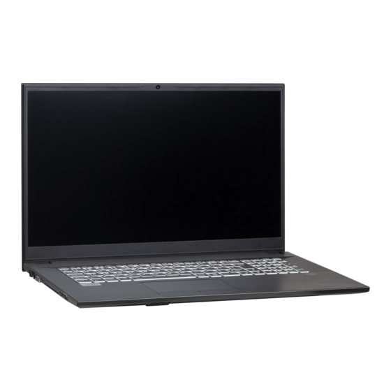
- Page 1 NJ70CU...
- Page 3 Preface Notebook Computer NJ70CU Service Manual...
- Page 4 Preface Notice The company reserves the right to revise this publication or to change its contents without notice. Information contained herein is for reference only and does not constitute a commitment on the part of the manufacturer or any subsequent ven- dor.
- Page 5 This manual is intended for service personnel who have completed sufficient training to undertake the maintenance and inspection of personal computers. It is organized to allow you to look up basic information for servicing and/or upgrading components of the NJ70CU se- ries notebook PC.
- Page 6 Preface IMPORTANT SAFETY INSTRUCTIONS Follow basic safety precautions, including those listed below, to reduce the risk of fire, electric shock and injury to per- sons when using any electrical equipment: 1. Do not use this product near water, for example near a bath tub, wash bowl, kitchen sink or laundry tub, in a wet basement or near a swimming pool.
- Page 7 Preface Instructions for Care and Operation The notebook computer is quite rugged, but it can be damaged. To prevent this, follow these suggestions: Don’t drop it, or expose it to shock. If the computer falls, the case and the components could be damaged. Do not expose the computer Do not place it on an unstable Do not place anything heavy...
- Page 8 Preface Avoid interference. Keep the computer away from high capacity transformers, electric motors, and other strong mag- netic fields. These can hinder proper performance and damage your data. Take care when using peripheral devices. Use only approved brands of Unplug the power cord before peripherals.
- Page 9 Preface Battery Precautions • Only use batteries designed for this computer. The wrong battery type may explode, leak or damage the computer. • Do not continue to use a battery that has been dropped, or that appears damaged (e.g. bent or twisted) in any way. Even if the computer continues to work with a damaged battery in place, it may cause circuit damage, which may possibly result in fire.
- Page 10 Preface Related Documents You may also need to consult the following manual for additional information: User’s Manual on CD/DVD This describes the notebook PC’s features and the procedures for operating the computer and its ROM-based setup pro- gram. It also describes the installation and operation of the utility programs provided with the notebook PC. System Startup 1.
-
Page 11: Table Of Contents
Preface Contents Introduction ..........1-1 Top ....................A-3 Bottom ................... A-4 Overview ..................1-1 LCD ....................A-5 Specifications ..................1-2 Dummy ODD ................. A-6 External Locator - Top View with LCD Panel Open ......1-4 HDD ....................A-7 External Locator - Front & Right Side Views .........1-5 Second HDD .................. - Page 12 Preface USB Charger/Audio Conn............B-24 Card Reader & LAN_RTL8411B ..........B-25 M Key PCIE SSD ................. B-26 M.2 Card ..................B-27 Audio Codec ................. B-28 CCD, MIC, LID, I/O Conn ............B-29 KBC ITE IT5570 ................B-30 VDD3/VDD5 ................B-31 3V, 5V, 3VS, 5VS, 1.8VS CTL ...........
-
Page 13: Introduction
Chapter 1: Introduction Overview This manual covers the information you need to service or upgrade the NJ70CU series notebook computer. Information about operating the computer (e.g. getting started, and the Setup utility) is in the User’s Manual. Information about dri- vers (e.g. -
Page 14: Specifications
Introduction Specifications Processor Options Video Adapter Intel® Core™ i7 Processor Intel UHD Graphics 620 i7-10510U (1.80GHz) Dynamic Frequency 8MB Smart Cache, 14nm, DDR4-2666MHz, TDP 15W Intel Dynamic Video Memory Technology Intel® Core™ i5 Processor Microsoft DirectX®12 Compatible Latest Specification Information i5-10210U (1.60GHz) Pointing Device 6MB Smart Cache, 14nm, DDR4-2666MHz, TDP 15W... - Page 15 Introduction Interface Environmental Spec One USB 3.2 Gen 2 Type-C Port* Temperature ° ° Operating: 5 C - 35 (Factory Option) One USB 3.2 Gen 2 Type-C Port* with Non-Operating: -20°C - 60°C Power Delivery (DC-In) Relative Humidity *The maximum amount of current supplied by USB Type-C Operating: 20% - 80% ports is 500mA (USB 2.0)/1500mA (USB 3.1).
-
Page 16: External Locator - Top View With Lcd Panel Open
Introduction External Locator - Top View with LCD Panel Open Figure 1 Top View 1. PC Camera 2. *PC Camera LED *When the PC camera is in use, the LED will be illuminated in white. 3. Built-In Array Microphone 4. LCD 5. -
Page 17: External Locator - Front & Right Side Views
Introduction External Locator - Front & Right Side Views Figure 2 Front View 1. LED Indicators 2. Multi-in-1 Card Reader FRONT VIEW Figure 3 Right Side View 1. 2-In-1 Audio Jack (Headphone and Microphone) 2. Microphone-In RIGHT SIDE VIEW Jack 3. -
Page 18: External Locator - Left Side & Rear View
Introduction External Locator - Left Side & Rear View Figure 4 Left Side View 1. DC-In Jack 2. RJ-45 LAN Jack 3. External Monitor LEFT SIDE VIEW Port 4. USB 3.2 Gen 2 Type-C Port *(Factory Option) USB 3.2 Gen 2 Type-C Port with Power Delivery 5. -
Page 19: External Locator - Bottom View
Introduction External Locator - Bottom View Figure 6 Bottom View 1. Battery 2. Vent 3. Speakers Overheating To prevent your com- puter from overhea- ting, make sure no- thing blocks any vent while the computer is in use. External Locator - Bottom View 1 - 7... -
Page 20: Mainboard Overview - Top (Key Parts)
Introduction Mainboard Overview - Top (Key Parts) Figure 7 Mainboard Top Key Parts 1 - 8 Mainboard Overview - Top (Key Parts) -
Page 21: Mainboard Overview - Bottom (Key Parts)
Introduction Mainboard Overview - Bottom (Key Parts) Figure 8 Mainboard Bottom Key Parts 1. CPU 2. Memory Slots DDR4 SO-DIMM 3. KBC-ITE IT5570 4. CMOS Battery Mainboard Overview - Bottom (Key Parts) 1 - 9... -
Page 22: Mainboard Overview - Top (Connectors)
Introduction Mainboard Overview - Top (Connectors) Figure 9 Mainboard Top Connectors 1. DC-In Jack 2. RJ-45 LAN Jack 3. External Monitor Port 4. USB 3.2 Gen 2 Type-C Port *(Factory Option) USB 3.2 Gen 2 Type-C Port with Power Delivery 5. -
Page 23: Mainboard Overview - Bottom (Connectors)
Introduction Mainboard Overview - Bottom (Connectors) Figure 10 Mainboard Bottom Connectors 1. ODD Connector 2. HDD Connector 3. Multi-in-1 Card Reader 4. M.2 Card Connector 5. Fan Connector 6. LCD Cable Connector 7. WLAN Connector 8. LTE Connector 9. SIM Card Reader 10. - Page 24 Introduction 1 - 12...
-
Page 25: Disassembly
Chapter 2: Disassembly Overview This chapter provides step-by-step instructions for disassembling the NJ70CU series notebook’s parts and subsystems. When it comes to reassembly, reverse the procedures (unless otherwise indicated). We suggest you completely review any procedure before you take the computer apart. -
Page 26: Maintenance Tools
Disassembly NOTE: All disassembly procedures assume that the system is turned OFF, and disconnected from any power supply (the battery is removed too). Maintenance Tools The following tools are recommended when working on the notebook PC: • M3 Philips-head screwdriver •... -
Page 27: Maintenance Precautions
Disassembly Maintenance Precautions The following precautions are a reminder. To avoid personal injury or damage to the computer while performing a removal and/or replacement job, take the following precautions: Power Safety Don't drop it. Perform your repairs and/or upgrades on a stable surface. If the computer falls, the case and other components Warning could be damaged. -
Page 28: Disassembly Steps
Disassembly Disassembly Steps The following table lists the disassembly steps, and on which page to find the related information. PLEASE PERFORM THE DISASSEMBLY STEPS IN THE ORDER INDICATED. To remove the Battery: To remove the 4G Module: 1. Remove the battery page 2 - 5 1. -
Page 29: Removing The Battery
Disassembly Removing the Battery Figure 1 Battery Removal 1. Turn off the computer, turn it over. 2. Slide the latch in the direction of the arrow (Figure 1a a. Slide the latch and hold it 3. Slide the latch in the direction of the arrow, and hold it in place (Figure 1b in place. -
Page 30: Removing The Hard Disk Drive
Disassembly Removing the Hard Disk Drive Figure 2 The hard disk drive can be taken out to accommodate other 2.5" serial (SATA) hard disk drives with a height of 7.0mm HDD Assembly (h). Follow your operating system’s installation instructions, and install all necessary drivers and utilities (as outlined in Removal Chapter 4 of the User’s Manual) when setting up a new hard disk. - Page 31 Disassembly 5. Remove screws from the HDD assembly (Figure 3d). Figure 3 6. Slightly lift and pull the hard disk assembly in the direction of arrow (Figure 3e HDD Assembly 7. Lift the hard disk assembly out of the bay (Figure 3f Removal (cont’d.) 8.
-
Page 32: Removing The System Memory (Ram)
Disassembly Removing the System Memory (RAM) Figure 4 RAM Module The computer has two memory sockets for 260 pin Small Outline Dual In-line Memory Modules (SO-DIMM) supporting Removal DDR4 2400MHz. The main memory can be expanded up to 32GB. The total memory size is automatically detected by the POST routine once you turn on your computer. - Page 33 Disassembly 5. Pull the latches to release the second module if necessary. 6. Insert a new module holding it at about a 30° angle and fit the connectors firmly into the memory slot. 7. The module will only fit one way as defined by its pin alignment. Make sure the module is seated as far into the slot as it will go.
-
Page 34: Removing The Keyboard
Disassembly Removing the Keyboard Figure 5 1. Turn off the computer, turn it over to remove the battery (page 2 - 10) and component cover (page 2 - Keyboard Removal 2. Locate the release points from the open bottom case (Figure 5a). -
Page 35: Removing The Optical (Cd/Dvd) Device
Disassembly Removing the Optical (CD/DVD) Device Figure 6 Optical Device 1. Turn off the computer, remove the battery (page 2 - 5), and bottom case (page 2 - Removal 2. Remove the screw and push the optical device out of the bay in the direction of the arrow (Figure 6a 3. -
Page 36: Removing The Wireless Lan Module
Disassembly Removing the Wireless LAN Module Figure 7 Wireless LAN 1. Turn off the computer, turn it over to remove the keyboard (page 2 - 10) and battery (page 2 - Module Removal 2. The Wireless LAN module will be visible at point on the mainboard (Figure 7a). -
Page 37: Wireless Lan, And Combo Module Cables
Disassembly Wireless LAN, and Combo Module Cables Note that the cables for connecting to the antennae on WLAN, WLAN & Bluetooth Combo modules are not labelled. The cables/covers (each cable will have either a black or transparent cable cover) are color coded for identification as outlined in the table below. -
Page 38: Removing The 4G Module
Disassembly Removing the 4G Module Figure 8 4G Module Removal 1. Turn off the computer, turn it over to remove the keyboard (page 2 - 10) and battery (page 2 - 2. The module will be visible at point on the mainboard (Figure 7a). -
Page 39: Removing The M.2 Ssd Module
Disassembly Removing the M.2 SSD Module Figure 9 M.2 SSD Module 1. Turn off the computer, turn it over to remove the keyboard (page 2 - 10) and battery (page 2 - Removal 2. The M.2 SSD module will be visible at point on the mainboard (Figure 9a). -
Page 40: Removing The Ccd
Disassembly Removing the CCD Figure 10 CCD Removal 1. Turn off the computer, turn it over to remove the keyboard (page 2 - 10) and battery (page 2 - 2. Run your fingers around the inner frame of the LCD panel at the points as indicated by the arrows (Figure a. - Page 41 Disassembly 4. Disconnect the cable (Figure 11f). Figure 11 5. Remove the CCD module (Figure 11g). CCD Removal 6. Reverse the process to install a new CCD module. (cont’d.) c. Disconnect the cable. d. Remove the CCD mod- ule. 6.
- Page 42 Disassembly 2 - 18...
-
Page 43: Part Lists
Appendix A:Part Lists This appendix breaks down the NJ70CU series notebook’s construction into a series of illustrations. The component part numbers are indicated in the tables opposite the drawings. Note: This section indicates the manufacturer’s part numbers. Your organization may use a different system, so be sure to cross-check any relevant documentation. -
Page 44: Part List Illustration Location
Part List Illustration Location The following table indicates where to find the appropriate part list illustration. Table A - 1 Part List Illustration Part Location page A - 3 page A - 4 Bottom page A - 5 page A - 6 Dummy ODD page A - 7 page A - 8... -
Page 45: Top
Figure A - 1 Top A - 3... -
Page 46: Bottom
Bottom Figure A - 2 Bottom A - 4 Bottom... -
Page 47: Lcd
Figure A - 3 LCD A - 5... -
Page 48: Dummy Odd
Dummy ODD Figure A - 4 Dummy ODD A - 6 Dummy ODD... -
Page 49: Dvd
Figure A - 5 DVD A - 7... -
Page 50: Hdd
Second HDD Figure A - 6 Second HDD A - 8 Second HDD... - Page 51 Figure A - 7 MB A - 9...
- Page 52 A - 10...
-
Page 53: Schematic Diagrams
Schematic Diagrams Appendix B: Schematic Diagrams This appendix has circuit diagrams of the NJ70CU notebook’s PCB’s. The following table indicates where to find the appropriate schematic diagram. Diagram - Page Diagram - Page Diagram - Page Table B - 1... - Page 54 Schematic Diagrams System Block Diagram &8 6\VWHP %ORFN 'LDJUDP &RPHW ODNH 8 &$''< %$< 6+((7 6+((7 &/,&. %2$5' '3 72 9*$ 6+((7 62 ',00B$B 6+((7 6+((7 6+((7 $8',2 %2$5' ';B9&&67* 9&&6)5B2& 9&&67 3RZHU 6+((7 6+((7 6<67(0 60%86 +'0, $8',2 %2$5' 62 ',00B%B 6+((7 6+((7...
-
Page 55: Processor 10/12
Schematic Diagrams Processor 1/12 0B$B'4> 0B%B'4> 8 & 0B$B'4 0B%B'4 0B$B&/.B''5 ''5 B&.1B ''5 B&.1B 0B%B&/.B''5 0B$B'4 ''5 B'4B ''5 B'4B 0B%B'4 ''5 B'4B ''5 B'4B ''5 B&.1B ''5 B&.1B ''5 B&.3B ''5 B&.3B 0B$B&/.B''5 ''5 B'4B ''5 B'4B ''5 B'4B ''5 B'4B ''5 B&.3B ''5 B&.3B 0B%B&/.B''5 0B$B'4... - Page 56 Schematic Diagrams Processor 2/12 '', 72 P'3 9*$ 3257 ('3 3$1(/ 9*$B 1 '', B7;1B ('3B7;1B ('3B7;1B 9*$B 3 '', B7;3B ('3B7;3B ('3B7;3B 9*$B 1 ('3B7;1B '', B7;1B ('3B7;1B 9*$B 3 ('3B7;3B '', B7;3B ('3B7;3B ',)) ('3B7;1B '', B7;1B ('3B7;1B '', B7;3B ('3B7;3B ('3B7;3B...
- Page 57 Schematic Diagrams Processor 3/12 9&&,2 &)* &)*B 569'B73B &)* 569'B73B &)*B &3 ,67B75,* &)*B &1 &)* 569'B73B &)*B &)* &)*B &)* &)* &)*B 569'B &)* &)*B 569'B &)* &)*B &)* &)*B &)* &)*B &)*B &)*B &)*B &)*B 569'B &)*B 569'B &)*>...
- Page 58 Schematic Diagrams Processor 4/12 63,B6&/. 63,B6&/. 63,B 63, B&6 60%B'$7$ 63, B&6 63,B6, 63,B6, 60%B&/. 63,B62 3&+B*33B& 63,B62 3&+B*33B& &ORVH WR 63, 730 3HWHU 63,B6&/. 60%B&/. &+ &. PLOB 63, B&/. *33B& 60%&/. 60%B&/.B''5 63,B62 60%B'$7$ PLOB &) &+ 60%B'$7B''5 63,B6, 63, B0,62 *33B&...
- Page 59 Schematic Diagrams Processor 5/12 3HWHU &38 &% 86% B 5;1 3&,(B5;1 B66' 3&,( B5;1 86% B B5;1 3&,( B5;1 86% B B5;1 &% 86% B 5;3 3&,(B5;3 B66' 3&,( B5;3 86% B B5;3 3&,( B5;3 86% B B5;3 & 9B; 5B 86% SRUW 7\SH &...
- Page 60 Schematic Diagrams Processor 6/12 %2$5'B,' && *33B% *63, B&6 && 3HWHU 730B3,54 3&+B*33B% *33B$ 3,54$ *63, B&6 &( &1 3&+B*33B% *33B% *63, B&/. *33B' ,6+B63,B&6 *63, B&6 &( &5 *33B% *63, B0,62 *33B' ,6+B63,B&/. *63, B&/. '(/ 3HWHU 3&+B*33B% &( &0 *33B% *63, B026,...
- Page 61 Schematic Diagrams Processor 7/12 &19L &5 &19,B:5B' 1 &19B:5B' 1 &3 &1 &19,B:5B' 3 &19B:5B' 3 *33B+ &38B& B*$7( &38B& B*$7( &0 &0 &19,B:5B' 1 &19B:5B' 1 *33B+ 7,0(6<1&B &1 &19,B:5B' 3 &19B:5B' 3 *33&B+ &) *33B+ ;7$/B)5(4B6(/(&7 &1 &1 &19,B:7B' 1 &19B:7B' 1 *33B+...
- Page 62 Schematic Diagrams Processor 8/12 %,26 3/7B567B57' /9& 3/7B567 WR %XIIHU 3/7B567 %8)B3/7B567 9&&67 +B9&&67B3:5*' $&( %(0 + 6/3B6 3/7B567 6/3B6 $&( %(0 + 3/7B567 6<6B5(6(7 *33B% 3/7567 *33B% 6/3B6 &1 6<6B5(6(7 *3' 6/3B6 686% B3&+ $//B6<6B3:5*' & 560567 560567 560567 *3' 6/3B6 686&...
- Page 63 Schematic Diagrams Processor 9/12 9&25( 69,' 9&&*7 9&&*7 69,' 9&&B&25( 9&&B&25( 9&&*7 9&&&25(B 9&&&25(B 9&&*7B 9&&*7B " " 9&&&25(B 9&&&25(B 9&&*7B 9&&*7B " " & & & & 9&&&25(B 9&&&25(B 9&&*7B 9&&*7B & " " 9&&&25(B 9&&&25(B 9&&*7B 9&&*7B & &...
- Page 64 Schematic Diagrams Processor 10/12 9''4 ),; 9''4 9&&,2 ),; 9&&,2 & & & & & & 9&&,2B287B 9''4B 9&&,2B287B 9''4B 9&&,2B287B 9''4B 9&&,2B287B & & 9''4B & & & 9&&,2B287B 9''4B 9&&,2B287B 9''4B $< 9&&,2B287B 9''4B 9&&,2B287B 9''4B 9&&,2B287B 9''4B &38 9&&,2B287B &38...
- Page 65 Schematic Diagrams Processor 11/12 9&&35,0B 3 &% 9&&35,0B 3 9&&35,0B 3 B 9&&B57& 9&&35,0B 3 9B; 6B & 9&&35,0B 3 9B; 6B %< & 9&&35,0B 3 &38 &$ & 9B; 5B 9&&35,0B 3 9&&57& &38 %< && 9&&35,0B 3 &38 9&&35,0B 3 B 9B;...
- Page 66 Schematic Diagrams Processor 12/12 &5 %< &) 966B 966B 966B 966B 966B 966B 966B 966B 966B 966B 966B 966B %< &% 966B 966B 966B 966B 966B 966B &3 &0 %< &) 966B 966B 966B 966B 966B 966B &0 966B 966B 966B 966B 966B...
- Page 67 Schematic Diagrams DDR4 SO_DIMM_0 9''4 9''4B977 -B',00$$ -B',00$% 0B$B'4> 0B$B'4 0B$B&/.B''5 &. B7 0B$B'4 0B$B&/.B''5 &. B& 0B$B'4 0B$B&/.B''5 &. B7 0B$B'4 0B$B&/.B''5 &. B& 0B$B'4 0B$B'4 9''4 W> >K^ dK ^K /DD 0B$B&.( &.( 0B$B'4 0B$B&.( &.( 0B$B'4 0B$B'4 ',00 B&+$B(9(17 0B$B&6 0B$B'4...
- Page 68 Schematic Diagrams DDR4 SO_DIMM_1 9''4B977 9''4 -B',00%$ -B',00%% 0B%B'4> 0B%B'4 0B%B&/.B''5 &. B7 62 ',00 % 0B%B'4 0B%B&/.B''5 &. B& 0B%B'4 0B%B&/.B''5 &. B7 0B%B'4 0B%B&/.B''5 &. B& 0B%B'4 0B%B'4 0B%B&.( &.( 0B%B'4 0B%B&.( &.( 0B%B'4 0B%B'4 0B%B&6 0B%B'4 W> >K^ dK ^K /DD 9''4 0B%B&6...
-
Page 69: Panel, Inverter
Schematic Diagrams Panel, Inverter 3$1(/ &211(&725 3$1(/ 32:(5 3/9'' H'3 SDQHO & -B/&' 9B; 5B 23(1B $ B$OH[ 9/(' & 9B; 5B ('3B7;1B & 9B; 5B ('3B7;3B & 9B; 5B ('3B7;1B & & 9B; 5B ('3B7;3B 9B; 5B & & 9B;... -
Page 70: Kbl Rtd2168
Schematic Diagrams KBL RTD2168 &57 -B&57 '5 1 '5 1 96B&57 '$&B5(' )&0 )5(' & '$&B*5((1 )&0 )*51 '$&B%/8( )&0 )%/8( & & & & & & 9*$B6'$ 9*$B+6<1& 9*$B+6B5 9*$B96<1& 9*$B96B5 9*$B6&/ & & & & & 9B; 5B &... -
Page 71: Pd Function
Schematic Diagrams PD Function $B$OH[ -'&B$& -B'&B-$&. & -'&B$& & 3& '& * 3& 3& 86%9&& % =$ $216 $216 7<3(& ,1 (0& 3& 9B; 5B Sheet 18 of 46 PD Function & & & 6,1.B&75/B(& 6,1.B&75/ 86%9&& ! ! ! !!DMFWP!DP/ ! ! ! !!DMFWP!DP/ ! ! ! !!DMFWP!DP/ 7LWOH... -
Page 72: Hdmi
Schematic Diagrams HDMI +'0, &211(&725 : 2 /(9(/6+,)7 +'0,B 96 & -B+'0, 9287 9B; 5B & & & +'0,B+3' & +27 3/8* '(7(&7 %< 3/$7)520 %< 3/$7)520 +'0,B6'$ & ''& &(& *1' +'0,B6&/ & 6&/ 5(6(59(' 70'6B&/2&. 70'6B&/2&. +'0,B&(& 70'6B&/2&. - &(&... -
Page 73: Hdd, Odd, Led, Tpm
Schematic Diagrams HDD, ODD, LED, TPM +'' &211(&7 2'' &211(&7 -B2'' 6$7$7;3 B5 & 9B; 5B 6$7$B7;3 B2'' 6$7$7;1 B5 & 9B; 5B 6$7$B7;1 B2'' -B+'' 6$7$5;1 B5 & 9B; 5B 6$7$B5;1 B2'' 6$7$5;3 B5 B6$7$7;3 B5 & 9B; 5B &... -
Page 74: Type-C
Schematic Diagrams Type-C $60B 86%9&& $60B 3HWHU B$OH[ 86%9&& B9&211B(1 $60B &&B5'< $60B B3:5B(1 0&B5'< & & B3:5B(1 B02'(B6(/ +&B5'< & 9B; 5B 9B; 5B B$OH[ & & & '()$8/7 7UDFH OHQJWK ',6&+$5*(B&75/ B,B6(/ $B85;1B6: $B85;1B6: ,B6(/ 08;B(1 '$BD B5;1 B5 $B85;3B6: B5;1 B5... - Page 75 Schematic Diagrams M Key PCIE SSD 1*))B0 3&,( 3RUW -B66' & & & 0 066' )25 237$1( 6833257 9B; 5B 3('(7 1& 3&,H *1' 6$7$ 1& 686&/. .K] 2 0 .(< 0 066' 0 066' 0 066' 1& &/.B3&,(B66' 5()&/.3 1&...
- Page 76 Schematic Diagrams USB Charger/Audio Conn. 3257 &KDUJH 86%B''B21 : 2 86% &+$5*(5 86%B3:5B(1 86%9&&B&+ 86%B31 B5 : 2 86% &+$5*(5 86%B31 : 2 86% &+$5*(5 86%B33 B5 86%B33 9287 : 2 86% &+$5*(5 & & 9B; 5B 9B; 5B 2& B$OH[ &+$5*(5 PRKP...
- Page 77 Schematic Diagrams Card Reader & LAN_RTL8411B &U\VWDO 6,=( 6ZLWFKLQJ 5HJXODWRU FORVH WR 3,1 PHHW UHDOWHN )UHT WROHUDQFH &$5' 5($'(5 ;7$/ 5(*287 PLOBVKRUWB $9'' -B&$5' 5(9 &D &E 6'B' 06B' B5 PLOBVKRUWB )25 6 :$.( 83 21 /$1 & & &' '$7 ;7$/ 6'B&0' 06B' B5...
-
Page 78: M Key Pcie Ssd
Schematic Diagrams M Key PCIE SSD 1*))B0 3&,( 3RUW 6$7$ B 6$7$ B -B66' & & & )25 237$1( 6833257 9B; 5B 6$7$*3 3('(7 1& 3&,H *1' 6$7$ 1& 686&/. .K] 2 0 .(< B$OH[ 3&,(B:$.( 1& &/.B3&,(B66' 5()&/.3 1& 6$7$ B 3&,(B:$.(B57' &/.B3&,(B66'... -
Page 79: M.2 Card
Schematic Diagrams M.2 Card 1*))B% 0 * /7( &$5' * /7( * /7( * /7( * /7( -B * & & + B % B ' B &21),*B 1*)) FRQQHFWRU SLQ LV GHILQHG DV QHHGLQJ WR VXSSRUW P$ 3LQ FRQWLQXRXV &21),*B 686&/. -
Page 80: Audio Codec
Schematic Diagrams Audio Codec +&% $8',2 &2'(& $/& & 9B; 5B & 9B; 5B > +($'3+21(B5 $8'* +($'3+21(B/ $8'* %((3B5 &/26( 72 &2'(& 3& %((3 0,& B95()2B/ ' B$OH[ E >K' /'/d > & &6 )25 92/801 6/((9( 96B$8' %((3 $'-867 9B;... -
Page 81: Ccd, Mic, Lid, I/O Conn
Schematic Diagrams CCD, MIC, LID, I/O Conn 7 3 &RQQHFW /,' 6:,7&+ 3HWHU IROORZ Q DGG /,' 3HWHU 73B9&& -B/,' /,'B6: B$OH[ BVKRUW /,'B6: /,' ,& 9$8/( )25 5()(5(1&( %< 352-(&7 0RGLI\ 5 (& SXOO XS & 9B; 5B $9/& -B73 &... -
Page 82: Kbc Ite It5570
Schematic Diagrams KBC ITE IT5570 (&B9'' ' B$OH[ '(%8* 3257 PLOBVKRUWB .%&B$9'' +&% 237,21 &/. & &/. 9B; 5B 3HWHU '(%8* 'HEXJ XVH 9B; 5B (0& )63,B .%&B$*1' (&B9'' 3&% )RRWSULQW PLO VKRUW S 86%B3:5B(1 &RQQHFW 9$8/( )25 5()(5(1&( %< 352-(&7 &... -
Page 83: Vdd3/Vdd5
Schematic Diagrams VDD3/VDD5 (1B 9 (1B 9 3& &9 9B; 5B 3& 3& 3& 23(1 95(* 3& 3& 3& 3& 3& 3& 9B; 5B 95(* 3*22' 3& 3& Sheet 30 of 46 9%67 9%67 9B; 5B % 58.5 9B; 5B 6<6 9 '59+ '59+... -
Page 84: 3V, 5V, 3Vs, 5Vs, 1.8Vs Ctl
Schematic Diagrams 3V, 5V, 3VS, 5VS, 1.8VS CTL ''B21 686% 686% 686% ''B21 & 686% & ''B21 9B132B 9B; 5B & & 9B; 5B 9B; 5B Sheet 31 of 46 & & &7 &7 9B; 5B 9B; 5B 3V, 5V, 3VS, 5VS, &... -
Page 85: 1.05Dx Vccstg, Vccsfr, Vccst
Schematic Diagrams 1.05DX VCCSTG, VCCSFR, VCCST 127( ';B9&&67* 7RQ QHHG 78521 21 7,0( 6+257 9&&67* 9&&67* 9287 B8 9287 & & & 9&&67*B(1 9B; 5B 3& 9&&6)5B2& &RPELQH ZLWK 7& 6= 9$ 8 &38B& B*$7( 9%,$6 9B; 5B 3& Sheet 32 of 46 &... - Page 86 Schematic Diagrams VDDQ, VDDQ_VTT 3& 3& 3& 9''4 9''4B977 & 9''4B5 %5= 8 3& 3& 9B; 5B 9''4B977 9/'2,1 9%67 9''4B'59+B5 9B; 5B 977B0(0B5 9''4B'59+ 9''4 '59+ 9''4B5 23(1 PP %&,+3 9''4B/ 977*1' 3& 3& PLO VKRUW S 23(1 PP 977B616 9''4B'59/ 9B;...
- Page 87 Schematic Diagrams 1.05VA 977B6(/(&7 977 95 2XWSXW 9ROWDJHV KLJK 6B977 9$B3:5*' 3& 3& 3& 9$B3:5*' 9''B $B%67 9''B $B%67B5 3& 9B; 5B %&,+3 0 1/ 9''B $B6: 1& 3&% )RRWSULQW %&,+3 1& 23(1B PP 6+257 6< 5$& 9'' B(1 9''B $B)% 23(1 &9...
-
Page 88: 1.8V, 2.5V
Schematic Diagrams 1.8V, 2.5V 3& 95(* 3& 9B; 5B 9B; 5B 3& 9B; 5B $'-) 9&17/ 23(1 PP 9$B3*' 9287 &9 1& 3& 3& 3& 3& -803 00 3& Sheet 35 of 46 6/3B686 1.8V, 2.5V & & 3& 3& 3&... -
Page 89: Mp2979 Controller
Schematic Diagrams MP2979 Controller 95$&38B3:0 95$&38B3:0 95B9'' 95B(1 95$&38B3:0 95$&38B3:0 3HWHU &9 95$&38B3:0 3& XB 9B; 5B 95$&38B3:0 (&B*3,2 $//B6<6B3:5*' 95$*7B3:0 95$*7B3:0 95$6$B3:0 95$6$B3:0 95$&38B3( & (&B*3,2 95$B67% 3& 95$B67% XB 9B; 5B 9&&67 95$&38B&6 95$&38B&6 95$&38B&6 95$&38B&6 95$&38B&6 95$&38B&6 *1'B6,*1$/ 95$*7B&6 3&... -
Page 90: Vccin, Vccgt, Vccsa Output
Schematic Diagrams VCCIN, VCCGT, VCCSA Output ( &$3 (0& (0& (0& (0& (0& 3HWHU 3& 3& 3& &R OD\ (0& (0& (0& (0& (0& 3& 3& 3& &*/7 = 9&& 3& XB 9B; 5B %67B3:0 $*1' 9&&B&25( 3& 95$&38B3:0 XB 9B; 5B 6:B3:0 95$B97(03 97(3 )/7... -
Page 91: Vccio, 2.5V
Schematic Diagrams VCCIO, 2.5V 3HWHU &38B& &9 &38B& B*$7( 3& 9&&,2 9B; 5B 3& 3& 3& 9&&,2 %&,+3 0 1/ 9&&,2B5 3&% )RRWSULQW %&,+3 3& 3& 3& 3& 3& '()$8/7 6+257 9287 *' = 3HWHU 3& 9B; 5B 3& 6+257 9B;... -
Page 92: Charger, Dc In
Schematic Diagrams Charger, DC IN 60$57 &+$5*(5 ,/,0 8/75$62 8/75$62 +&% 3& 3& & 3& 3& 3& 3& 3& 3& 3& 3& 3& 3& 3& 9B; 5B BVKRUW BVKRUW 3& 3& %$7'59 9B; 5B 3& 3& 3& 3& 9B; 5B 9B;... -
Page 93: Lid Sw Board
Schematic Diagrams LID SW Board /,' 6:,7&+ %2$5' /-B/,' /B/,'B6: /,' 6: %2$5' /B*1' Sheet 40 of 46 LID SW Board /,' 6: %2$5' & & /B/,'B6: 9&& /B& 175 * 9B; 5B /,' 6: %2$5' /& /,' 6: %2$5' + B ' B + B ' B + B ' B... -
Page 94: Odd To Hdd Caddy Bay
Schematic Diagrams ODD to HDD Caddy Bay 2'' 72 +'' %2$5' &$1'< %$< &DGG\ ED\ 6$7$ 3RUW %,26 6$7$ 3RUW 'HIDXOW &RQQHFW 607 &RQQHFW '-B2'' '-B+'' '2''B7;3 '2''B7;1 '2''B5;1 '2''B5;3 + B ' B Sheet 41 of 46 'B 96 ODD to HDD Caddy &... -
Page 95: Click Board
Schematic Diagrams Click Board &/,&. %2$5' 3&%$ &+(&. &&5 &&5 &&5 &&5 Sheet 42 of 46 &-B73 &73%87721B5 B$OH[ &&5 &&5 Click Board &73%87721B/ &/,&. %2$5' & & &*1' &6: &6: 7 %-% &73%87721B5 7 %-% &73%87721B/ && &/,&. %2$5' &&... -
Page 96: Audio Board
Schematic Diagrams Audio Board $8',2 %2$5' &21 3257 $B86%9&& $B86%9&& &21 3257 '()$8/7 $B86%9&& $B86%9&& $B86%9&& $B86%9&& $B86%9&& $B86%9&& $& $& $& $& $& $& $& $& $& $& 9B; 5B $& $& $& 9287 $8',2 %2$5' $& 9B; 5B 9287 $*1' $8',2 %2$5'... -
Page 97: Power Sw Board
Schematic Diagrams Power SW Board 32:(5 6:,7&+ 3:B6: B(0, %-B6: %& Sheet 44 of 46 9B; 5B 3:B6: %0B%71 Power SW Board 3: 6: %*1' %*1' & & 3:B6: 3:B6: %*1' %*1' 32:(5 21 /(' + B ' B + B ' B + B ' B 3&%$ &+(&. -
Page 98: Rgb Kb
Schematic Diagrams RGB KB 5*% .% 2QO\ 5*%.%B3:5 -B.%/(' & 9B; 5B &8B5*% &8B5*% &8B5*% .% '(7 .%=21(B% .%=21(B5 &8B5*% .%=21(B* 5*%.%6:B5 .%=21(B5 J[[[PBU .% /(' 5*% (&B3:0B/('.%B5 &8B5*% .% /(' 5*% 5*%.%6:B* .%=21(B* Sheet 45 of 46 .% /(' 5*% RGB KB (&B3:0B/('.%B* .% /(' 5*%... -
Page 99: Power Seq
Schematic Diagrams Power Seq. 32:(5 6(4 57&9&& 6WDWXV W3&+ 9FF57& VWDEOH WR 57&B567 KLJK ! 57&B567 $& ,1 6WDWXV B/'2 3:5B6: 3RZHU RQ 6WDWXV 9$B(&B(1 ''B21 Sheet 46 of 46 Power Seq. & & 560567 686& 9''4 686% 9''4B977 $//B6<6B3:5*' 9&&6$ +B95B5($'<... - Page 100 Schematic Diagrams B - 48...
Need help?
Do you have a question about the NJ70CU and is the answer not in the manual?
Questions and answers