Advertisement
Quick Links
AR0140CS2C00SUEAH3-GEVB
AR0140CS Evaluation Board
User's Manual
Evaluation Board Overview
The evaluation boards are designed to demonstrate the features of
ON Semiconductor's image sensors products. This headboard is
intended to plug directly into the Demo 3 system. Test points and
jumpers on the board provide access to the clock, I/Os, and other
miscellaneous signals.
Features
•
Clock Input
Default – 27 MHz Crystal Oscillator
♦
Optional Demo 3 Controlled MClk
♦
•
Two Wire Serial Interface
Selectable Base Address
♦
•
Parallel Interface
•
HiSPi (High Speed Serial Pixel) Interface
•
MIPI Interface
•
ROHS Compliant
Block Diagram
© Semiconductor Components Industries, LLC, 2015
September, 2015 − Rev. 0
Figure 2. Block Diagram of AR0140CS2C00XUEAH3−GEVB
EVAL BOARD USER'S MANUAL
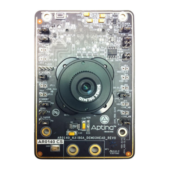
Figure 1. AR0140CS Evaluation Board
1
www.onsemi.com
Publication Order Number:
EVBUM2309/D
Advertisement

Related Manuals for ON Semiconductor AR0140CS2C00SUEAH3-GEVB


Summary of Contents for ON Semiconductor AR0140CS2C00SUEAH3-GEVB
- Page 1 Evaluation Board Overview The evaluation boards are designed to demonstrate the features of www.onsemi.com ON Semiconductor’s image sensors products. This headboard is intended to plug directly into the Demo 3 system. Test points and EVAL BOARD USER’S MANUAL jumpers on the board provide access to the clock, I/Os, and other miscellaneous signals.
-
Page 2: Bottom View
AR0140CS2C00SUEAH3−GEVB Top View RESET Switch SW1 Parallel O/p P6 CLK Sel P19 TEST P5 C Bypass P24 EEPROM ADDR Sel P27 FLASH P7 ATEST P14 I/O Voltage Sel P16 STANDBY P8 C ADDR Sel P4 HiSPi Mode Sel P18 Figure 3. Top View of Evaluation Board − Default Jumpers Bottom View Baseboard Connector J1 Figure 4. - Page 3 AR0140CS2C00SUEAH3−GEVB Jumper Pin Location The jumpers on headboards start with Pin 1 on the leftmost side of the pin. Grouped jumpers increase in pin size with each jumper added. Pin 1 Pins 1−4 Figure 5. Pin Locations for a Single Jumper. Pin 1 is Located at the Leftmost Side and Increases as it Moves to the Right Pin 1 Pins 1 and 2...
- Page 4 When Pushed, 240 ms Reset Signal will be Sent to AR0140CS Interfacing to ON Semiconductor Demo 3 Baseboard Table 2. SHORTED JUMPERS FOR POWER The ON Semiconductor Demo 3 baseboard has a similar MEASUREMENT 52-pin connector which mates with J1 of the headboard. Jumper...
- Page 5 AR0140CS2C00SUEAH3−GEVB References All design files; schematics, board design images, Gerber files, as well as the BOM file can be found here: http://www.onsemi.com/PowerSolutions/product.do?id=A R0140CS www.onsemi.com...
-
Page 6: Technical Support
onsemi, , and other names, marks, and brands are registered and/or common law trademarks of Semiconductor Components Industries, LLC dba “onsemi” or its affiliates and/or subsidiaries in the United States and/or other countries. onsemi owns the rights to a number of patents, trademarks, copyrights, trade secrets, and other intellectual property. A listing of onsemi’s product/patent coverage may be accessed at www.onsemi.com/site/pdf/Patent−Marking.pdf.
Need help?
Do you have a question about the AR0140CS2C00SUEAH3-GEVB and is the answer not in the manual?
Questions and answers