Telit Wireless Solutions WE310F5-I Hardware User's Manual
Hide thumbs
Also See for WE310F5-I:
- Hardware user's manual (60 pages) ,
- Reference manual (40 pages) ,
- Quick start manual (19 pages)

Subscribe to Our Youtube Channel
Related Manuals for Telit Wireless Solutions WE310F5-I


Summary of Contents for Telit Wireless Solutions WE310F5-I
- Page 1 WE310F5-I/P Module Hardware User Guide 1VV0301662 Rev. 16 – 2021-10-01 Telit Technical Documentation 1VV0301698 2021-01 Rev.0...
- Page 2 WE310F5-I/P Module Hardware User Guide APPLICABILITY TABLE PRODUCTS WE310F5-I WE310F5-P 1VV0301662 Rev. 16 Page 2 of 41 2021-10-01 Not Subject to NDA...
-
Page 3: Table Of Contents
WE310F5-I/P Module Hardware User Guide CONTENTS INTRODUCTION Scope Audience Contact Information, Support Symbol Convention Related Documents GENERAL PRODUCT DESCRIPTION Overview Product Variants and Frequency Bands Block Diagram FEATURES Main Features PIN ALLOCATION PIN-Out General Purpose I/O SAR ADC Characteristics Pad Layout... - Page 4 WE310F5-I/P Module Hardware User Guide ESD Characteristics MECHANICAL DESIGN WE310F5-I WE310F5-P PCB Pad Design PCB Pad Dimensions Stencil Solder Paste PCB Pad Dimensions PACKAGING Tray Moisture sensitivity CONFORMITY ASSESSMENT ISSUES FCC/IC Regulatory Notices FCC/IC Compliance SAFETY RECOMMENDATIONS GLOSSARY DOCUMENT HISTORY 1VV0301662 Rev.
-
Page 5: Introduction
This document describes electrical specifications, mechanical information, interfaces application, and manufacturing information about the Telit WE310F5-I/P Wi-Fi/BLE module. With the help of this document and other application notes or user guides, users can understand the Telit WE310F5-I/P Wi-Fi/BLE module well and develop various products quickly. Audience This document is intended for Telit customers, especially system integrators, about to implement their applications using the Telit module. -
Page 6: Related Documents
WE310F5-I/P Module Hardware User Guide Related Documents Module Name Description 80664ST11034A WE310F5-I/P AT Command Reference Guide 1VV0301663 WE310F5-I/P EVB Hardware User Guide Table 1: Related documents 1VV0301662 Rev. 16 Page 6 of 41 2021-10-01 Not Subject to NDA... -
Page 7: General Product Description
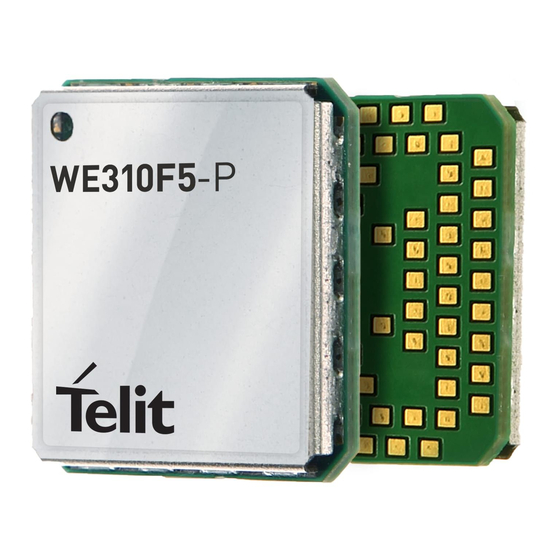
2. GENERAL PRODUCT DESCRIPTION Overview The WE310F5-I/P is a module with a single-band Wi-Fi/BLE (5.0) 2.4GHz combo module that provides an easy and cost-effective way for users to add wireless connectivity to their products. This module is available in two different factors the antenna version named WE310F5-I with 15mmx18mm dimensions and an on-board multilayer antenna and the WE310F5-P with 13.1mmX14.3mm with antenna pad. -
Page 8: Block Diagram
[HE] WE310F5-I/P Block Diagram The following figure shows a high-level block diagram of the WE310F5-I/P module and its major functional blocks. Figure 2: Telit WE310F5-I/P module block diagram 1VV0301662 Rev. 16 Page 8 of 41... -
Page 9: Features
Internal Co-existence mechanism between Wi-Fi and BLE to share the same antenna Temperature Operating: -40°C ~ 85°C Range Junction: -40°C ~ 105°C Storage: -55°C ~ 125°C Table 2: Main Features The WE310F5-I/P module supports the following peripherals Interfaces. Item Peripherals Comment UART UART0 Low Power Mode Wakeup AUX_UART LOG UART/Low power mode wakeup (no Flow control)). - Page 10 WE310F5-I/P Module Hardware User Guide The sample size for Stereo & 5.1 channel: 16-bit, 24-bit 32 bit. PCM not supported WAKEUP Wake up from deep sleep USB 2.0 CDC class device 12-bit SAR ADC Single ended input Range: 0~3.3V 12- or 24-hour format (seconds, minutes, hours,...
-
Page 11: Pin Allocation
WE310F5-I/P Module Hardware User Guide 4. PIN ALLOCATION PIN-Out All IO’s are in LVTTL 3.3V logic. Signal Function Comment Pull-down Restriction Primary serial port RXD0 Serial data Input (RXD) >1K AA15 TXD0 Serial data Output (TXD) >1K CTS0 Input for Clear to send >1K... - Page 12 WE310F5-I/P Module Hardware User Guide Miscellaneous RESET pin Active low WAKEUP WAKEUP Module from >1K sleep Audio DVI_WA0 I2S Frame Sync DVI_RX I2S RX DVI_TX I2S TX DVI_CLK I2S CLK Power Supply VBATT_3V3 Main power supply 3.3V Power VBATT_3V3 Main power supply 3.3V...
- Page 13 WE310F5-I/P Module Hardware User Guide Power Ground Power Debug Port (SWD) SWD_CLK SWD_CLK SWD_DATA SWD_DATA Bootstrap pin. LOW for SWD RESERVED RESERVED RESERVED RESERVED RESERVED RESERVED RESERVED RESERVED RESERVED RESERVED RESERVED RESERVED RESERVED RESERVED RESERVED RESERVED RESERVED RESERVED RESERVED RESERVED...
-
Page 14: General Purpose I/O
WE310F5-I/P Module Hardware User Guide General Purpose I/O Module by default has 5 dedicated GPIO’s (IO1 ~ IO5). The remaining GPIO’s are multiplexed with other interfaces. Signal Name GPIO Number IO1/I2C_SCL IO2/I2C_SDA IO3/SD_CMD IO4/SD_CLK IO5/SD_D0 SPI_INT/IO6 RXD0 AA15 TXD0 CTS0... -
Page 15: Sar Adc Characteristics
VBAT=1.62~3.63V Table 7: SAR ADC Characteristics Pad Layout The Pad layout for both (WE310F5-I and WE310F5-P) versions of the module is the same, the only difference is the dimension of the module as WE310F5-I has the onboard antenna. The following figures show the pad layout: Figure 5: Telit WE310F5-I Pads Layout Top View 1VV0301662 Rev. - Page 16 WE310F5-I/P Module Hardware User Guide Figure 6: Telit WE310F5-I PIN Out Legend Figure 7: Telit WE310F5-P Pads Layout Top View Figure 8: Telit WE310F5-P PIN Out Legend 1VV0301662 Rev. 16 Page 16 of 41 2021-10-01 Not Subject to NDA...
-
Page 17: Power Supply
5. POWER SUPPLY Power Supply Requirements The WE310F5-I/P can be directly supplied by a 3.3V power supply source capable of at least 500mA or higher. The voltage supply to all the required parts of the chipset is provided by an embedded switching regulator. -
Page 18: Average Power Consumption
WE310F5-I/P Module Hardware User Guide Average power consumption The table below shows the current consumption in different states. These measurements are obtained from a DC power analyzer. Power Consumption Typical Average (mA) Standby 0.003 Idle (Radio OFF, UART ON) 14.3 Deep Sleep (Radio OFF) (no Wi-Fi Association) 0.04... - Page 19 WE310F5-I/P Module Hardware User Guide QPSK MCS1_40 12.7 QPSK MCS2_40 12.7 16QAM MCS3_40 12.2 16QAM MCS4_40 12.2 64QAM MCS5_40 11.7 64QUAM MCS6_40 11.7 64QAM MCS7_40 11.7 Table 12: WLAN Continuous Tx Power consumption Danger: The equipment must be supplied by an external limited power source in compliance with clause 2.5 of the standard EN 60950-1.
-
Page 20: Rf Specification
WE310F5-I/P Module Hardware User Guide 6. RF SPECIFICATION Wi-Fi Tx Power The Wi-Fi Transmit power at RF pad at 25 °C @3.3V. To measure WE310F5-P power, remove the antenna and connect a pigtail to the RF pad. Wi-Fi 2G4 / CH 6... -
Page 21: Ble Tx Power
WE310F5-I/P Module Hardware User Guide Wi-Fi 2G4 / CH 6 Modulation Data Rates Sensitivity (dBm) Standard 802.11x 11 Mbps BPSK 6 Mbps BPSK 9 Mbps QPSK 12 Mbps QPSK 18 Mbps 16 QAM 24 Mbps 16 QAM 36 Mbps 64 QAM... -
Page 22: Design Guidelines
Figure 9: Telit WE310F5 Sample Circuit A voltage translator must be used if the components are interfacing with Telit components have digital signals with higher I/O interface voltage than the WE310F5-I/P module. Using voltage translator components in your design makes the system ready for operation at the full VIO voltage range, 3.3V to system I/O voltage. -
Page 23: Power Supply Design Guidelines
PC. It is recommended to connect the WE310F5-I/P ON* (N16 pin) to control the Enable pin of the level shifter, in this way a tri-state will be guarantee during BOOT. -
Page 24: Bypass Capacitors
Another example is for GSM, in general, you can use 33pF 0402 or 56pF 0201 General Design Rules The WE310F5-I has an embedded ceramic antenna. To preserve the bandwidth, keep attention to not place any copper or mechanical component in front or close to the ceramic antenna. - Page 25 WE310F5-I/P Module Hardware User Guide Figure 11: WE310F5-I Placement Example For the WE310F5-I version the antenna is placed directly on the board, so you will need to leave a copper keep-out area as shown below: Figure 12: WE310F5-I Placement Example showing no copper in any layer of the board.
-
Page 26: Audio
(G-CPW) line. Figure 15: Coplanar Waveguide Dimensioning Example The final dimensions depend on the use of stack-up. While the WE310F5-I is already tuned to the embedded antenna, the WE310F5-P version needs to be tuned in relationship to the stack-up used. -
Page 27: Audio Considerations
WE310F5-I/P Module Hardware User Guide Audio considerations Since, components and PCBs are getting smaller while the component’s density increases, another problem that becomes important is heat dissipation. For that reason, pay special attention to the PCB stack-up and component placement. -
Page 28: Esd Characteristics
Figure 17: Layout Example for FAST Digital Lines Lines to resolve this, add in parallel, to 10nF, another capacitor of about 10pF to 33pF. ESD Characteristics Refer to the table below for ESD characteristics of the WE310F5-I/P modules. Human Body Model (HBM) ±2000 Charge Device Model ±... -
Page 29: Mechanical Design
WE310F5-I/P Module Hardware User Guide 8. MECHANICAL DESIGN The following is the Top and bottom view of the Telit WE310F5-I module WE310F5-I Figure 18: WE310F5-I bottom view Figure 19: WE310F5-I side view and mechanical design 1VV0301662 Rev. 16 Page 29 of 41... -
Page 30: We310F5-P
WE310F5-I/P Module Hardware User Guide WE310F5-P Figure 20: WE310F5-I bottom view Figure 21: WE310F5-P side view and mechanical design PCB Pad Design For the solder pads, it is recommended to use Non-Solder Mask Defined pad (NSMD) on the PCB. Figure 22: SMD and NSMD Pad 1VV0301662 Rev. -
Page 31: Pcb Pad Dimensions
WE310F5-I/P Module Hardware User Guide PCB Pad Dimensions It is not recommended to place via or micro-via not covered by the solder resist in an area of 0.3 mm around the pads unless it carries the same signal of the pad itself as shown below. -
Page 32: Pcb Pad Dimensions
Note/Tip: All temperatures refer to the topside of the package, measured on the package body surface. Danger: The WE310F5-I/P module withstands only one reflow process. The above solder reflow profile represents the typical SAC reflow limits and does not guarantee adequate adherence of the module to the customer application throughout the temperature range. -
Page 33: Packaging
9. PACKAGING Tray The WE310F5-I/P modules are packaged on trays of 50 pieces each when small quantities are required (i.e. for test and evaluation purposes). These trays are not designed for use in SMT processes for pick and place handling. -
Page 34: Moisture Sensitivity
WE310F5-I/P Module Hardware User Guide Moisture sensitivity The WE310F5-I/P module is classified as a LEVEL 3 moisture-sensitive device following IPC/JEDEC J-STD-020. Moreover, the customer must take care of the following conditions: a. The shelf life of the product inside the dry bag is 12 months starting from the bag seal date when stored in a non-condensing atmospheric environment of <... -
Page 35: Conformity Assessment Issues
WE310F5-I/P Module Hardware User Guide 10. CONFORMITY ASSESSMENT ISSUES FCC/IC Regulatory Notices Hereby, Telit Communications S.p.A declares that the WE310F5-I/P Module is following Directive 2014/53/EU. The full text of the EU declaration of conformity is available at the following internet http://www.telit.com\red... - Page 36 WE310F5-I/P Module Hardware User Guide FCC Class B digital device notice This equipment has been tested and found to comply with the limits for a Class B digital device, pursuant to part 15 of the FCC Rules. These limits are designed to provide reasonable protection against harmful interference in a residential installation.
- Page 37 WE310F5-I/P Module Hardware User Guide Omnidirectional 2.3dBi@2.4GHz band Label and compliance information The product has FCC ID and ISED label on the device itself. Also, the OEM host end product manufacturer will be informed to display a label referring to the enclosed module.
-
Page 38: Safety Recommendations
WE310F5-I/P Module Hardware User Guide 11. SAFETY RECOMMENDATIONS Be sure the use of this product is allowed in the country and the environment required. The use of this product may be dangerous and must be avoided in the following areas: •... -
Page 39: Glossary
WE310F5-I/P Module Hardware User Guide 12. GLOSSARY Acronym Definition Universal Serial Bus High Speed UART Universal Asynchronous Receiver Transmitter Bluetooth low energy WLAN Wireless LAN Serial Peripheral Interface Analog – Digital Converter Digital – Analog Converter Pulse Width Modulation Input Output... -
Page 40: Document History
Pinout and some figures. Updated Pinout figures, Addition of details to Table 7 2020-09-01 General Power Consumption and Deleted figures - WE310F5-I Top View and WE310F5-P Top View. 2020-06-29 Update of SD card, Clock, and Memory specification. 2020-05-27 First issue. - Page 41 Telit Technical Documentation 1VV0301698 2021-01 Rev.0...
Need help?
Do you have a question about the WE310F5-I and is the answer not in the manual?
Questions and answers