Telit Wireless Solutions WE310F5-I Hardware User's Manual
Hide thumbs
Also See for WE310F5-I:
- Hardware user's manual (54 pages) ,
- Reference manual (40 pages) ,
- Quick start manual (19 pages)
Advertisement
Quick Links
Advertisement

Subscribe to Our Youtube Channel
Related Manuals for Telit Wireless Solutions WE310F5-I


Summary of Contents for Telit Wireless Solutions WE310F5-I
- Page 1 WE310F5-I/P Module Hardware User Guide 1VV0301662 Rev 2 – 2020-09-01...
- Page 2 WE310F5-I/P Module Hardware User Guide SPECIFICATIONS ARE SUBJECT TO CHANGE WITHOUT NOTICE NOTICE While reasonable efforts have been made to assure the accuracy of this document, Telit assumes no liability resulting from any inaccuracies or omissions in this document, or from use of the information obtained herein.
- Page 3 WE310F5-I/P Module Hardware User Guide USAGE AND DISCLOSURE RESTRICTIONS License Agreements The software described in this document is the property of Telit and its licensors. It is furnished by express license agreement only and may be used only in accordance with the terms of such an agreement.
- Page 4 WE310F5-I/P Module Hardware User Guide APPLICABILITY TABLE PRODUCTS WE310F5-I WE310F5-P 1VV0301662 Rev 2 Page 4 of 60 2020-09-01...
- Page 5 WE310F5-I/P Module Hardware User Guide Contents NOTICE……………..................2 COPYRIGHTS ....................2 COMPUTER SOFTWARE COPYRIGHTS ............2 USAGE AND DISCLOSURE RESTRICTIONS ..........3 CONTENTS ....................5 FIGURE LIST ....................7 TABLE LIST ....................8 INTRODUCTION ................9 Scope ................... 9 Audience..................
- Page 6 WE310F5-I/P Module Hardware User Guide PINS ALLOCATION ..............27 Pin-out ..................27 Pads Layout ................33 DESIGN GUIDELINES ............... 35 General Digital Interface Recommendations ....... 35 Power circuitry ................36 Bypass Capacitors ..............36 Antenna Guidelines ..............37 Audio considerations ..............40 Other General Design Considerations ........
- Page 7 Figure 25: Inhibit Area for Not Solder Covered Vias ............47 Figure 26: Solder Reflow Profile ..................48 Figure 27: WE310F5-I/P Packaging example (to replace with the final one and add the WE310F5-P figure ) ...................... 50 1VV0301662 Rev 2...
- Page 8 WE310F5-I/P Module Hardware User Guide TABLE LIST Table 1: Feature Description Table ................16 Table 2: Peripherals Interfaces ..................17 Table 3: GPIO Alternate Pinmux Table ................. 18 Table 4: Power Supply requirements ................20 Table 5: Input/output Levels ..................20 Table 6: Timing Specification-Power Sequence ............
- Page 9 WE310F5-I/P Module Hardware User Guide INTRODUCTION Scope The aim of this document is to describe some of the hardware solutions useful for developing a product with the Telit WE310F5-I/P Wi-Fi/BLE module. Audience This document is intended for Telit customers, who are integrators, about to implement their applications using our WE310F5-I/P modules.
- Page 10 WE310F5-I/P Module Hardware User Guide Text Conventions Danger – This information MUST be followed, or catastrophic equipment failure or bodily injury may occur. Caution or Warning – Alerts the user to important points about integrating the module, if these points are not followed, the module and end user equipment may fail or malfunction.
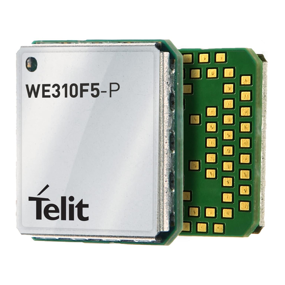
- Page 11 PRODUCT DESCRIPTION Overview The WE310F5-I/P is a module with single band Wi-Fi/BLE(5.0) 2.4GHz combo module that provides an easy and cost-effective way to the users to add wireless connectivity to their products. This module is available in two different from factors the antenna version named WE310F5-I with 15mmx18mm dimensions and an on-board multilayer antenna and the WE310F5-P with 13.1mmX14.3mm with antenna PAD.
- Page 12 (SL) Integracija WE310F5-I/P modula v uporabniški aplikaciji bo morala upoštevati projektna navodila, opisana v tem priročniku. (SP) La utilización del modulo WE310F5-I/P debe ser conforme a los usos para los cuales ha sido deseñado descritos en este manual del usuario.
- Page 13 WE310F5-I/P Module Hardware User Guide Block Diagram Following is the block diagram: Figure 3: WE310F5-I/P Block Diagram 1VV0301662 Rev 2 Page 13 of 60 2020-09-01...
- Page 14 WE310F5-I/P Module Hardware User Guide FEATURE DESCRIPTION Main Features 1. Highly integrated single chip with low power single band (2.4GHz) Wireless LAN (WLAN) and Bluetooth Low Energy (BLE5.0) communication controller. 2. Dedicated ArmV8-M Cortex-M33 (KM4) processor + low power Armv8-M Cortex-M23 (KM0) WLAN (802.11 b/g/n) MAC, an 1T1R capable WLAN baseband, RF, Bluetooth...
- Page 15 WE310F5-I/P Module Hardware User Guide Item Description USB 2.0 HS/FS/LS mode Internal DMA support 1.5Kbyte built-in\bulk out buffers Master/slave modes SPI (High Speed) master/slave up to 50 MHz Dynamic bit-rate clock UART Format 1 start bi/, 7/8 bits, 0/1 parity and 1/2 Stop...
- Page 16 One programmable alarm with interrupt function. The alarm can be triggered by any combination of the time fields Digital calibration circuit Register write protection Key-Matrix Table 1: Feature Description Table The WE310F5-I/P module supports the following peripherals Interfaces. Item Peripherals Comment UART LP_UART1...
- Page 17 WE310F5-I/P Module Hardware User Guide EXT_32K EXT_32K LP_TIM4_TRIG LP_TIM4_TRIG Timer Capture LP_TIM5_TRIG LP_TIM5_TRIG Time Capture LP_I Standard/fast/high speed mode (up to 3.33Mbps) SDIO 1-Bit SDIO mode Maximum 25 MHz Clock SD HOST Maximum 25 MHz Clock HS_PWM0~17 LP_PWM0~5 Support Low Power Mode X5...
- Page 18 WE310F5-I/P Module Hardware User Guide Please refer to documents for more detail. General Purpose I/O The module has 6 GPIO which can be configured as Input \ Output or as Alternate Function. Following table provides the GPIO numbers and their alternate functions with direction and Internal PU/PD at startup.
- Page 19 WE310F5-I/P Module Hardware User Guide 5. Multi-channel DMA support 6. Multi sampling trigger sources a. Software b. Timer 7. 1 low power voltage comparator for battery voltage measurement 8. Conversion item control or another FIFO level trigger wakeup 1VV0301662 Rev 2...
- Page 20 WE310F5-I/P Module Hardware User Guide POWER SUPPLY Power Supply Requirements The WE310F5-I/P is directly supplied by using a 3.3V power supply source. The voltage supply to all the required parts of the chipset is provided by an embedded switching regulator.
- Page 21 WE310F5-I/P Module Hardware User Guide Figure 4: Power UP Sequence Symbol Parameter Minimum Typical Maximum Unit VDDX ready time PRDY Internal ring clock stable time after VD1833 ready LP core power CORE ready time HS MCU boot time boot Shutdown occurs 0.5*VDD...
- Page 22 WE310F5-I/P Module Hardware User Guide Figure 5: Shutdown Sequence Power Consumption Power Consumption Typical Average [mA] Standby Idle (Radio OFF, UART ON) Deep Sleep (Radio OFF) 0.02 DTIM=1 @ 2.4G DTIM=3 @ 2.4G DTIM=10 @ 2.4G BLE RX (peak current, connected to BT BLE TX (@ RF pad’s xxdBm @1Mbps)
- Page 23 WE310F5-I/P Module Hardware User Guide 5.5 Mbps 11 Mbps BPSK 6 Mbps BPSK 9 Mbps QPSK 12 Mbps QPSK 18 Mbps 16 QAM 24 Mbps 16 QAM 36 Mbps 64 QAM 48 Mbps 64 QAM 54 Mbps BPSK MCS0_20 QPSK...
- Page 24 WE310F5-I/P Module Hardware User Guide Wi-Fi 2G4 / CH 6 Modulation Data Rates RF Output IEEE EVM Standard 802.11x (dBm) (dB) Limit (dB) WE310F5-I/P* BPSK 1 Mbps QPSK 2 Mbps 5.5 Mbps 11 Mbps BPSK 6 Mbps BPSK 9 Mbps...
- Page 25 WE310F5-I/P Module Hardware User Guide Wi-Fi 2G4 / CH 6 Modulation Data Rates RF Output IEEE EVM Standard 802.11x (dBm) (dB) Limit (dB) WE310F5-I/P* 64 QAM MCS5_40 64 QAM MCS6_40 64 QAM MCS7_40 Table 9: IEEE 802.11 EVM @2.4GHz * for P version remove the antenna and apply a pigtail to the hot pad.
- Page 26 WE310F5-I/P Module Hardware User Guide Wi-Fi 2G4 / CH 6 Modulation Data Rates Sensibility IEEE EVM Standard 802.11x (dBm) Limit (dB) 16 QAM 24 Mbps 16 QAM 36 Mbps 64 QAM 48 Mbps 64 QAM 54 Mbps BPSK MCS0_20 QPSK...
- Page 27 WE310F5-I/P Module Hardware User Guide PINS ALLOCATION Pin-out Signal Function Type Comment Asynchronous Serial Port (USIF0) – Prog. / Data + HW Flow Control RXD0 Serial data output (RXD) to DTE LVTTL 3.3V Serial data input (TXD) from AA15 TXD0 LVTTL 3.3V...
- Page 28 WE310F5-I/P Module Hardware User Guide I2C ( SCL ) Configurable GPIO01 LVTTL 3.3V SD (CMD) alternate I2C ( SDA) Configurable GPIO02 LVTTL 3.3V SD (CLK) alternates SD ( DO ) Configurable GPIO03 LVTTL 3.3V alternate DVI Fn enable as Configurable GPIO04 LVTTL 3.3V...
- Page 29 WE310F5-I/P Module Hardware User Guide RF Section WIFI/BT Main Antenna (50 ohm) ANTENNA Miscellaneous Functions Input Command for Module CMOS 1.8V Active high Enable WAKEUP WAKEUP Module from Idle LVTTL 3.3V TBD if could be implemente Audio Section DVI_WA0 TBD if I2S Digital Audio Interface LVTTL 3.3V...
- Page 30 WE310F5-I/P Module Hardware User Guide RF Ground Power RF Ground Power RF Ground Power RF Ground Power RF Ground Power RF Ground Power RF Ground Power RF Ground Power RF Ground Power RF Ground Power Thermal Ground Power Thermal Ground...
- Page 31 WE310F5-I/P Module Hardware User Guide Thermal Ground Power Thermal Ground Power Thermal Ground Power Thermal Ground Power Power Ground Power Power Ground Power Power Ground Power Power Ground Power Power Ground Power Debug Port (SWD) RESERVED SWD_CLK RESERVED SWD_DATA RESERVED...
- Page 32 WE310F5-I/P Module Hardware User Guide RESERVED RESERVED RESERVED RESERVED RESERVED RESERVED RESERVED RESERVED RESERVED RESERVED RESERVED RESERVED RESERVED RESERVED RESERVED RESERVED RESERVED RESERVED RESERVED RESERVED RESERVED RESERVED RESERVED RESERVED RESERVED RESERVED RESERVED RESERVED RESERVED RESERVED RESERVED RESERVED RESERVED RESERVED RESERVED...
- Page 33 *Reserved Pins must not be connected. Pads Layout The Pads layout for both (WE310F5-I and WE310F5-P) the versions of the module is the same, the only difference is the dimension of the RAW PCB due to the on-board antenna on the WE310F5-I version of the module Following figure shows the pads layout configuration for the module: Figure 6: Pads Layout Top View –...
- Page 34 WE310F5-I/P Module Hardware User Guide Figure 7: Pads Layout Top View – WE310F5-P Figure 8: Pinout Legend Color-WE310F5-I/P 1VV0301662 Rev 2 Page 34 of 60 2020-09-01...
- Page 35 PC. It is recommended to connect the WE310F5-I/P ON* pin to control the EN pin of the level shifter, in this way a tri-state will be guarantee duting the BOOT-UP activity.
- Page 36 WE310F5-I/P Module Hardware User Guide Power circuitry It is important to provide to the module a clean power supply source. We recommend adding and external EMI filter to improve the quality of the power supply especially when the module will be embedded with other technologies, (i.e. Cellular).
- Page 37 Figure 11: Placement Example-Please place the module aligning the PCB outline of the module with that one of the EVK For WE310F5-I version the antenna is placed directly on the board, so you will need to leave a copper cutout area as shown in below:...
- Page 38 WE310F5-I/P Module Hardware User Guide Figure 12: Placement Example and Cutout copper area for WE310F5-I-Please place and remove the copper in any layer of the board. For WE310F5-P you will need to use an external antenna connected to the antenna pad of the module through an SMA connector placed to the board as shown in figure 13.
- Page 39 (G-CPW) line. Figure 15: Coplanar Waveguide Dimensioning Example The final dimensions depend on the use of stack-up. While the WE310F5-I is already tuned to the embedded antenna, the WE310F5-P version needs to be tuned in relationship to the stack-up used.
- Page 40 WE310F5-I/P Module Hardware User Guide ANT1 Antenna_PAD Figure 16: Minimal RF Matching Network Circuitry A possible network topology is seen in the above figure and it consist of three passive components. To reuse Telit’s FCC certification for our module, the antenna on the application board...
- Page 41 WE310F5-I/P Module Hardware User Guide 6. Use one layer for horizontal lines only, and the another one for vertical lines. Fill the remaining empty space with ground. 7. Use several vias to connect all ground planes and areas in all layers with possible through hole drills.
- Page 42 WE310F5-I/P Module Hardware User Guide 1VV0301662 Rev 2 Page 42 of 60 2020-09-01...
- Page 43 WE310F5-I/P Module Hardware User Guide MECHANICAL DESIGN WE310F5-I Figure 18: WE310F5-I Mechanical Design Figure 19: WE310F5-I Side View 1VV0301662 Rev 2 Page 43 of 60 2020-09-01...
- Page 44 WE310F5-I/P Module Hardware User Guide Figure 20: WE310F5-I Recommended Land Pattern 1VV0301662 Rev 2 Page 44 of 60 2020-09-01...
- Page 45 WE310F5-I/P Module Hardware User Guide WE310F5-P Figure 21: WE310F5-P Mechanical Design Figure 22: WE310F5-P Side View 1VV0301662 Rev 2 Page 45 of 60 2020-09-01...
- Page 46 WE310F5-I/P Module Hardware User Guide Figure 23: WE310F5-P Recommended Land Pattern PCB Pad Design For the solder pads, it is recommended to use Non-Solder Mask Defined pad (NSMD) on the PCB. Figure 24: SMD and NSMD Pad PCB Pad Dimensions It is not recommended to place via or micro-via not covered by solder resist in an area of 0.3 mm around the pads unless it carries the same signal of the pad itself as shown below.
- Page 47 WE310F5-I/P Module Hardware User Guide Figure 25: Inhibit Area for Not Solder Covered Vias The holes in pad are allowed only for blind holes and not for through holes. Table 14: shows the recommended PCB pad surfaces Finish Layer thickness [µm] Properties 3 –7 / 0.03 –...
- Page 48 WE310F5-I/P Module Hardware User Guide Solder Reflow Figure 26: and Table 16: shows the recommended solder reflow profile. Figure 26: Solder Reflow Profile Profile Feature Pb-Free Assembly Average ramp-up rate (T to T 3 °C/second max. Preheat • 150 °C Temperature Min.
- Page 49 All temperatures refer to topside of the package, measured on the package body surface. WARNING: The WE310F5-I/P module withstands only one reflow process. The above solder reflow profile represents the typical SAC reflow limits and does not guarantee adequate adherence of the module to the customer application throughout the temperature range.
- Page 50 WE310F5-I/P Module Hardware User Guide PACKAGING Tray The WE310F5-I/P modules are packaged on trays of 50 pieces each when small quantities are required (i.e. for test and evaluation purposes). These trays are not designed for use in SMT processes for pick and place handling.
- Page 51 WE310F5-I/P Module Hardware User Guide Moisture Sensitivity The WE310F5-I/P module is classified as a LEVEL 3 moisture sensitive device in accordance with IPC/JEDEC J-STD-020. Moreover, the customer must take care of the following conditions: a) The shelf life of the product inside the dry bag is 12 months starting from the bag seal date, when stored in a non-condensing atmospheric environment of <...
- Page 52 WE310F5-I/P Module Hardware User Guide CONFORMITY ASSESSMENT ISSUES FCC/IC Regulatory Notices Hereby, Telit Communications S.p.A declares that WE310 F5-I/P Module is following Directive 2014/53/EU. The full text of the EU declaration of conformity is available at the following internet address: http://www.telit.com\red...
- Page 53 WE310F5-I/P Module Hardware User Guide FCC/IC COMPLIANCE Modification statement Telit has not approved any changes or modifications to this device by the user. Any changes or modifications could void the user’s authority to operate the equipment. Telit n’approuve aucune modification apportée à l’appareil par l’utilisateur, quelle qu’en soit la nature.
- Page 54 WE310F5-I/P Module Hardware User Guide radio communications. However, there is no guarantee that interference will not occur in a particular installation. If this equipment does cause harmful interference to radio or television reception, which can be determined by turning the equipment off and on, the...
- Page 55 WE310F5-I/P Module Hardware User Guide The product has a FCC ID label on the device itself. Also, the OEM host end product manufacturer will be informed to display a label referring to the enclosed module. The exterior label will read as follows: “Contains Transmitter Module FCC ID: xxx” or “Contains FCC ID: xxx”.
- Page 56 WE310F5-I/P Module Hardware User Guide SAFETY RECOMMENDATIONS Read Carefully Be sure the use of this product is allowed in the country and in the environment required. The use of this product may be dangerous and must be avoided in the following areas: •...
- Page 57 WE310F5-I/P Module Hardware User Guide ACRONYMS TTSC Telit Technical Support Centre Universal Serial Bus High Speed Data Terminal Equipment UMTS Universal Mobile Telecommunication System WCDMA Wideband Code Division Multiple Access HSDPA High Speed Downlink Packet Access HSUPA High Speed Uplink Packet Access...
- Page 58 WE310F5-I/P Module Hardware User Guide Complementary Metal – Oxide Semiconductor CMOS Master Output – Slave Input MOSI Master Input – Slave Output MISO Clock MRDY Master Ready SRDY Slave Ready Chip Select Real Time Clock Printed Circuit Board Equivalent Series Resistance...
- Page 59 Update of SD card, Clock and Memory specification. 2020-09-01 Updated Pinout figures, Addition of details to Table 7 General Power Consumption and Deleted figures - WE310F5-I Top View and WE310F5-P Top View. 1VV0301662 Rev 2 Page 59 of 60 2020-09-01...
Need help?
Do you have a question about the WE310F5-I and is the answer not in the manual?
Questions and answers