
Related Manuals for CIS VISION:elite VCC-F52U25CL


Summary of Contents for CIS VISION:elite VCC-F52U25CL
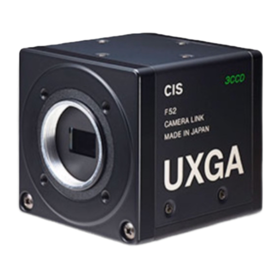
- Page 1 VCC-F52U25CL Rev.900-668-31-01 English UXGA 3CCD Color Camera Link Camera VCC-F52U25CL Product Specification & Operational Manual CIS Corporation ©2010 CIS Corporation. All rights reserved.
-
Page 2: Table Of Contents
Remote Interface Function ......................17 10. Initial Settings ..........................18 11. CCD Optical Axis Accuracy ......................19 12. Dimensions ..........................20 13. Cases for Indemnity (Limited Warranty)..................21 14. CCD Pixel Defect........................21 15. Product Support ........................21 ©2010 CIS Corporation. All rights reserved. -
Page 3: Scope Of Application
With a rise in temperature, color of the sticker goes to black. The circle for 60 must be kept white. (Please be noted that once the sticker color turns to black, it won’t be back to white again.) <Example>:Ambient temperature +45℃ (113 degrees F), calm →Installed on an aluminum board. (120×200×5mm) ©2010 CIS Corporation. All rights reserved. - Page 4 The rising time of camera power supply voltage shall be less than +10V, Max 60ms. Please avoid noises like chattering when rising. Voltage Rising Time [ ms ] In case of abnormal operation, contact the distributor from whom you purchased the product. ©2010 CIS Corporation. All rights reserved.
-
Page 5: Product Outline
Please refer to the timing chart for the details. RGB 24bit/30bit are selectable. □ Bundled Items Camera □ CIS Control Panel Software (For evaluation and demonstration purpose). ※ □ Please ask for the details or download it from our web. ※ ©2010 CIS Corporation. All rights reserved. -
Page 6: Specification
1/1,000, 1/1,500, 1/2,500, 1/5,000, 1/10,000, 1/54,000s (18) Pulse Width: 1/15~1/8,000s (Trigger input pulse width: 2,504H (max)~2H (min)) variable range Manual Shutter: 1/30(Off)~1/54,000s ・Fixed Trigger Shutter Mode ・Pulse Width Trigger Mode Trigger shutter mode (19) ©2010 CIS Corporation. All rights reserved. - Page 7 ※Camera functions can operate normally under operation guaranteed temperature. Humidity RH 20~80% with no condensation -25℃ ~ +60℃ Temperature Storage environment (23) Humidity RH 20~80% with no condensation ©2010 CIS Corporation. All rights reserved.
-
Page 8: Camera Output Signal Specification
5 seconds shall be waited after turning on power to get proper camera operation. ※ +5.0V(VCC) 100Ω TTL Output HD74LV1GT32ACME (RENESA) Voh:3.8V(Min) Vol:0.55V(Max) 100Ω TTL Input HD74LV1GT14ACME (RENESAS) Vt-:0.5(Min) Vt+:1.9V(Max) 12pins circular connector at rear, GPIO Interface ©2010 CIS Corporation. All rights reserved. -
Page 9: Ccd Spectral Response (Representative Value)
VCC-F52U25CL Rev.900-668-31-01 4.3 . CCD Spectral Response (Representative Value) 4.3.1. CCD (ICX274AL) Spectral Response ※ Lens characteristics, IR cut filter, and luminous source characteristics are not considered. 4.3.2. Prism Spectral Transmission Characteristics ©2010 CIS Corporation. All rights reserved. -
Page 10: Function Settings
Address 009 MSB and address 010 LSB makes 16bit in total. Shutter speed = (1251 - (009&010))×26.27μ s+18.53μ s Max Data = 1251 Trigger Polarity 0: Positive Input 1: Negative Input Trigger Input 0: Camera Link (CC1) Input 1: 12pin Connector(11pin) Input ©2010 CIS Corporation. All rights reserved. - Page 11 Input 083 or 053 to save the data to EEP-ROM. Note: When setting the data with 2 Byte, High Byte shall be set first, then Low Byte to the next. ※ The camera rewrites the internal resister when receiving Low Byte. ©2010 CIS Corporation. All rights reserved.
-
Page 12: External Connector Pin Assignment
Pin No. Pin No. Xclk- Xclk+ Yclk- Yclk+ 100Ω SerTC+ SerTC- Terminated SerTFG- SerTFG+ CC1- CC1+ (Trigger IN -) (Trigger IN +) NC (CC2+) NC (CC2-) NC (CC3-) NC (CC3+) NC (CC4+) NC (CC4-) ©2010 CIS Corporation. All rights reserved. -
Page 13: Timing Chart
9 10 11 12 30 31 32 33 34 35 36 37 38 39 40 LVAL Output DVAL Output FVAL Output 9H(V Sync) 19H(Back proch) 1200H (Active Line Margin) (Active Line) Total = 1252H ©2010 CIS Corporation. All rights reserved. -
Page 14: Fixed Trigger Shutter Mode
Exposure Time Trigger invalid ✖ (Trigger Input ) ( Exposure Time ) ✖ SP Output (F) (Exposure Signal) Exposure Time (B) Exposure Time ( Register Set Value) (Register Set Value) Video Output (B) DVAL Output ©2010 CIS Corporation. All rights reserved. -
Page 15: Pulse Width Trigger Shutter Mode
(Trigger Input) SP Output (Exposure Time) (Exposure Signal) (B) Exposure Time Exposure Time Exposure Time (B) (Pulse Width) ( Pulse Width ) (Pulse Width) ( Video Output ( C)) ✖ Video Output DVAL Output ©2010 CIS Corporation. All rights reserved. -
Page 16: Partial Scan Mode Details
50 fps・ 480 H 756 H ・ ・ ・ ・ 768 H 948 H 40 fps ・ ・ ・ ・ 1026 H 1120 H 33 fps ・ ・ ・ ・ 1224 1252 H 30 fps ©2010 CIS Corporation. All rights reserved. -
Page 17: Remote Interface Function
To save the data into EEPROM, please refer to Section 5., Function Settings. C is the code to send the data back from the camera. Note: Do not set code C when sending the data from PC side. ©2010 CIS Corporation. All rights reserved. -
Page 18: Initial Settings
0: Camera Link (CC1) Input Output Data Select 0: 24bit RGB Output Data Gamma Mode 0: Gamma OFF (1.0) Partial Scan Mode 0: Full Frame Scan Mode Partial Scan Total Line 021&022 1251: Read Only ©2010 CIS Corporation. All rights reserved. -
Page 19: Ccd Optical Axis Accuracy
0.6 phai to the center of lens mount. Datum Plane A Inclination of effective pixels theta to datum plane A. Theta shall be under ±0.5° *)Dimensions from datum plane A to the center of the lens mount 910-010-00-00 (Unit:mm) ©2010 CIS Corporation. All rights reserved. -
Page 20: Dimensions
Label Position *) C Mount screws comply with ANSI/ASME B1.1, 1-32U (2B). *) Screw length from C mount lens surface shall be under 4.5mm. And protruding portion shall be less than 4.5mm. 999-502-00-02 (Unit :mm) ©2010 CIS Corporation. All rights reserved. -
Page 21: Cases For Indemnity (Limited Warranty)
On very rare occasions, however, CCD pixel defects might be noted with time of usage of the products. Cause of the CCD pixel defects is the characteristic phenomenon of CCD itself and CIS is exempted from taking any responsibilities for them.
Need help?
Do you have a question about the VISION:elite VCC-F52U25CL and is the answer not in the manual?
Questions and answers