Table of Contents
Advertisement
Quick Links
Advertisement
Table of Contents

Related Manuals for Texas Instruments ADC0XD1520RB


Summary of Contents for Texas Instruments ADC0XD1520RB
- Page 1 ADC0XD1520RB Reference Board Users’ Guide SNAU133 Page 1 ...
-
Page 2: Table Of Contents
1.2 Packing List 1.3 References 2.0 Quick Start 2.1 Installing the WaveVision 5 Software 2.2 Installing the ADC0XD1520RB Hardware 2.3 Launching the WaveVision 5 Software 2.4 WaveVision 5 – User Interface Overview 2.5 System / Device Configuration 2.6 Data Capturing 3.0 Secondary Panel Description... -
Page 3: Overview
The ADC0XD1520RB demonstrates a high-performance signal acquisition sub-system that achieves 7/8-bit resolution and corresponding SNR and dynamic range on two channels with sampling rates of at least 1.5 GS/s or one channel at a sampling rate of 3.0 GHz. The board showcases the following Texas Instruments devices: •... -
Page 4: Features
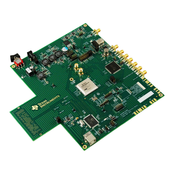
Single +12V power adapter input Simplicity and performance of USB 2.0 connection to the PC Functions with TI's latest WaveVision 5 signal-path control and analysis software 1.2 Packing List The ADC0XD1520RB kit consists of the following components: • ADC0XD1520RB Reference Board •... - Page 5 1.4 Board Orientation Q-ch. Sig. I-ch. Sig. Ext Clock DCLK_RST Ext. Trigger LEDs LMX2541 Int Clock ADC08D1520 Control Jumpers Power section +12V Controller Power FPGA (Xilinx Power Switch Auxiliary Data Port (FMC connector) on bottom Figure 1: ADC0XD1520RB Board Layout SNAU133 Page 5 ...
-
Page 6: Quick Start
Figure 2: Recommended lab setup. A filter may not be necessary on the clock if the generator is very clean (beyond -80dBm SFDR). 12V DC Signal Signal Generator Generator Bandpass Filter DC block Bandpass Balun Filter DC block ADC0xD1520RB 50Ω termination DC block 50Ω termination DC block USB2.0 SNAU133... -
Page 7: Installing The Wavevision 5 Software
7. Turn on the SW2 rocker power switch. Verify that the green LED (labeled LD10, near the J12 power jack) is lit. 8. Connect the supplied USB 2.0 cable from the PC USB port to the ADC0XD1520RB USB jack. SNAU133 ... - Page 8 2.3 Launch the WaveVision 5 Software. Start the WaveVision 5 software on your computer by selecting the desktop icon “WaveVision 5” or by clicking on the Start button, and selecting Start -> Programs -> WaveVision 5 -> WaveVision 5 The software will automatically detect the board and load the appropriate software profile and will proceed to download the controller firmware and FPGA code onto the reference board.
-
Page 9: Wavevision 5 - User Interface Overview
2.4 WaveVision 5 - User Interface Overview Figure 3: WaveVision 5 Example Window Figure 3 above shows the WV5 user interface panel (GUI). This is the top level interface panel. It is arranged in such a way that the plot is always in the middle. There are tabs arranged on each side of the window to give the user additional information or control of features. -
Page 10: System / Device Configuration
2.5 System / Device Configuration Prior to capturing data, confirm that the board is in the "ECE (Extended Control Enable)" mode, The ECE jumper is located in the ADC pin control jumper area. The board should be sent with this jumper in place. This means that the ADC will be controlled through the SPI interface and not with jumpers driving the control pins. - Page 11 2.5.1 Main Panel The main menu bar of the WaveVision 5 software has several control buttons as shown in Figures 4 and 5, which may be used to perform most tasks with a button click. 1 - Load Plot A new plot window is created and the Plot Load dialog is displayed. The selected plot file is loaded into the new window.
- Page 12 2.5.2 Plot Window Controls Figure 6: WaveVision 5 plot window controls 1 - Load Plot The Plot Load dialog is displayed, and the selected plot file is loaded into the new window. 2 - Save Plot Displays the Plot Save dialog (this button is only active when the plot contains one or more channels with data). 3 - Reset Zoom Reset X and Y axis zoom to 100%.
- Page 13 Figure 7a: WaveVision 5 main window command buttons Open the Signal Source panel on the right side of the window and confirm that the ADC0XD1520RB is available and confirm that it is selected. There are five possible modes of operation selectable here: •...
- Page 14 Note – When using “I and Q” mode, it is also necessary to select the Channels tab and deselect the “Automatically hide inactive channels” option box in order to allow both channels to appear on the plot. Alternatively, one channel may be displayed per plot: Figure 7b: I and Q mode –...
- Page 15 Figure 8: WaveVision 5 main window command buttons • Sampling Rate - When the signal source panel is selected, the clock frequency is displayed. This is initially the internal clock. In this example, 1500 MHz is generated by the LMX2541 on the reference board.
- Page 16 Next, configure the hardware (including the ADC) using the Registers control panel on the right side. This is the most important of all the panels for controlling the ADC0XD1520RB. This panel has seven sub-tabs that control the settings of the board and registers inside the ADC0XD1520. The seven sub-tabs are shown below and include;...
- Page 17 Config: This tab configures various features and modes of the ADC0XD1520 and is shown below. It accesses or changes the following functions, all of which are controlled through Configuration Register 1. Figure 10: Config Panel • nSD – Second DCLK output – When this bit is 1b, the device only has one DCLK output and one OR output.
- Page 18 Extended Config: This tab controls the extended configuration register. Figure 11: Extended Config Panel • TPO – Test Pattern Output – When this bit is set to 1b, the ADC is disengaged and a test pattern generator is connected to the outputs including OR. This test pattern will work with the device in the SDR, DDR, and the Non-demux Modes (DES and Non-DES).
- Page 19 I-channel: This tab changes the sign and the magnitude of the offset and the full scale range settings. Figure 12: I-Channel Panel • I-channel Offset Sign – This pull-down selects a positive or negative offset. • I-ch Offset – This slider selects the magnitude of I-ch Offset applied. Adjustment can be done using the computer mouse/pointer, or using left/right arrow keys once the slider has been selected.
- Page 20 Phase Adjust : This tab controls the Aperture Delay function. Figure 13: t Adjust Panel • POL – Polarity Select – When this bit is selected, the polarity of the ADC sampling clock is inverted • Coarse Phase Adjust – Sets the approximate amount of coarse Aperture Delay applied. •...
- Page 21 Figure 14: Temperature Panel • Ambient Temperature – Provides the local/board temperature of the LM95233 IC. • ADC Temperature – Provides the approximate die temperature of the ADC0XD1520. • FPGA Temperature – Provides the approximate die temperature of the Xilinx Virtex-4 FPGA. Note: No changes will appear until the Update Temperatures button is clicked.
-
Page 22: Data Capturing
2.6 Data Capturing The board is now ready for a data capture. Before proceeding, perform a manual calibration of the ADC. Even though the ADC performs a self-calibration at the time of power-up, it is recommended that the user perform another calibration after sufficient time has passed for the system (primarily temperature) to stabilize. - Page 23 {0.4Vpp, 2.0Vpp}. However, there is a significant insertion for the Teledyne relay, RF303, and other components on the ADC0XD1520RB, as shown in Figure 15. To compensate for this insertion loss, use the recommended values in Table 1. The magnitude shown is for the signal at J11, the External Clock Input SMA, in order to maintain the proper level at the ADC’s CLK+/- inputs.
-
Page 24: Reference Board Functional Description
7 or 8x2 Ctrlr. Virtex -4 FPGA DCLKI/Q FIFO I/F Vcmo SPI(1.8V) DCLK_RST+/- SE2DIFF SPI(3.3V) Ext Clock +3.3V/5V, Local Clock (96 MHz) USI-1 Conx.x2 for external devices Clk Gen uWire (LMX2541) Trigger SE2DIFF Figure 16: ADC0XD1520RB System Block Diagram SNAU133... -
Page 25: System Description
3230MHz. This output frequency from the VCO is divided to achieve the desired clocking frequency of the ADC. On the ADC0XD1520RB board, the device is configured for a 1.5 GHz output through the serial interface. The initial command sequence that automatically configures the LMX2541 is pre-programmed into the FPGA’s firmware. - Page 26 Install J155 to force FPGA to output data on FMC port (without a power good signal from Carrier to Mezzanine). This is useful when a non FMC compliant board is connected to Mezzanine (ADC0XD1520RB) • Install J156 to force a power good signal from Mezzanine (ADC0XD1520RB) to Carrier. This is used to override for initial FPGA debug. SNAU133...
- Page 27 J155 FMC_PG_C2M Override power good C2M (FPGA will output data on Mezzanine FMC) Carrier (ADC0xD1520RB) (ADC12D1X00RFRB) J156 FMC_PG_M2C Override power good M2C (indicates power good from Mez. to Carrier) Figure 18: Explanation of Power Good override jumpers for FMC port SNAU133 ...
- Page 28 Figure 19: Bottom of ADC0XD1520RB showing FMC port 2.8.4 LM95233 Temperature Sensor Using the TI LM95233 temp sensor chip; the ambient, ADC0XD1520 and Xilinx FPGA temperatures can be monitored. The temperature readings are available through the WV-5 software. SNAU133...
-
Page 29: Electrical Specification
3.0 Electrical Specification Power Supply: Nominal = 12V Minimum = 11.0V, Maximum = 12.5V (Voltages outside these levels can cause damage!!) Power Consumption: Nominal = 10 Watts Maximum = 20 Watts ADC Input Signals: Maximum Operating Voltage = see datasheet Recommended/initial (full scale) generator setting = 0 dBm (The maximum level at the signal generator is dependent upon the insertion loss from other hardware before the ADC inputs. - Page 30 EVALUATION BOARD/KIT/MODULE (EVM) ADDITIONAL TERMS Texas Instruments (TI) provides the enclosed Evaluation Board/Kit/Module (EVM) under the following conditions: The user assumes all responsibility and liability for proper and safe handling of the goods. Further, the user indemnifies TI from all claims arising from the handling or use of the goods.
- Page 31 For EVMs annotated as FCC – FEDERAL COMMUNICATIONS COMMISSION Part 15 Compliant Caution This device complies with part 15 of the FCC Rules. Operation is subject to the following two conditions: (1) This device may not cause harmful interference, and (2) this device must accept any interference received, including interference that may cause undesired operation.
- Page 32 Also, please do not transfer this product, unless you give the same notice above to the transferee. Please note that if you could not follow the instructions above, you will be subject to penalties of Radio Law of Japan. Texas Instruments Japan Limited (address) 24-1, Nishi-Shinjuku 6 chome, Shinjukku-ku, Tokyo, Japan http://www.tij.co.jp...
- Page 33 【ご使用にあたっての注意】 本開発キットは技術基準適合証明を受けておりません。 本製品のご使用に際しては、電波法遵守のため、以下のいずれかの措置を取っていただく必要がありますのでご注 意ください。 (1)電波法施行規則第6条第1項第1号に基づく平成18年3月28日総務省告示第173号で定められた電波暗 室等の試験設備でご使用いただく。 (2)実験局の免許を取得後ご使用いただく。 (3)技術基準適合証明を取得後ご使用いただく。 なお、本製品は、上記の「ご使用にあたっての注意」を譲渡先、移転先に通知しない限り、譲渡、移転できないも のとします。 上記を遵守頂けない場合は、電波法の罰則が適用される可能性があることをご留意ください。 日本テキサス・インスツルメンツ株式会社 東京都新宿区西新宿6丁目24番1号 西新宿三井ビル http://www.tij.co.jp...
- Page 34 EVALUATION BOARD/KIT/MODULE (EVM) WARNINGS, RESTRICTIONS AND DISCLAIMERS For Feasibility Evaluation Only, in Laboratory/Development Environments. Unless otherwise indicated, this EVM is not a finished electrical equipment and not intended for consumer use. It is intended solely for use for preliminary feasibility evaluation in laboratory/development environments by technically qualified electronics experts who are familiar with the dangers and application risks associated with handling electrical mechanical components, systems and subsystems.
- Page 35 TI products are designated by TI as compliant with ISO/TS 16949 requirements. Buyers acknowledge and agree that, if they use any non-designated products in automotive applications, TI will not be responsible for any failure to meet such requirements. Following are URLs where you can obtain information on other Texas Instruments products and application solutions: Products...
- Page 36 Mouser Electronics Authorized Distributor Click to View Pricing, Inventory, Delivery & Lifecycle Information: Texas Instruments ADC07D1520RB/NOPB...
Need help?
Do you have a question about the ADC0XD1520RB and is the answer not in the manual?
Questions and answers