Advertisement
Quick Links
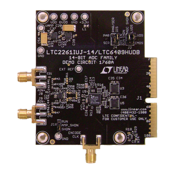
DESCRIPTION
Demonstration circuit 1760A supports a family of 14-
/12-bit 25Msps to 150Msps ADCs and an LTC
noise amplifier. Each assembly features a device from the
LTC2261-14 family of high dynamic range 1.8V ADCs and
a LTC6409 low noise amplifier.
Demonstration circuit 1760A supports the LTC2261-14
family full rate CMOS and DDR CMOS output mode. The
PERFORMANCE SUMMARY
PARAMETER
Supply Voltage—ADC
Supply Voltage—Amplifier
Analog Input Range
Logic Input Voltages
Logic Output Voltages (OV
= 1.8V)
DD
Sampling Frequency (Convert Clock Frequency)
Convert Clock Level
Convert Clock Level
Resolution
Input Frequency Range
SFDR
SNR
DEMO MANUAL DC1760A
12-/14-Bit, 25Msps to 150Msps
circuitry on the analog inputs is optimized for analog input
®
6409 low
frequencies from DC to 100MHz. Refer to the data sheet
for proper input networks for different input frequencies.
Design files for this circuit board are available at
http://www.linear.com/demo
L, LT, LTC, LTM, Linear Technology and the Linear logo are registered trademarks and PScope
and QuikEval are trademarks of Linear Technology Corporation. All other trademarks are the
property of their respective owners.
(T
= 25°C)
A
CONDITION
Depending on Sampling Rate and the A/D
Converter Provided, This Supply Must Provide Up
to 150mA
Depending on Supply Voltage Used, This Supply
Must Provide Up to 25mA
Depending On Sense Pin Voltage
Minimum Logic High
Maximum Logic Low
Minimum High Level Output Voltage
Maximum Low Level Output Voltage
Depending on ADC This Can Vary Between
20Msps and 125Msps
Single-Ended Encode Mode (ENC
–
Differential Encode Mode (ENC
Not Tied to GND) 0.2V to 3.6V
14 Bits
DC-100MHz
See Applicable Data Sheet
See Applicable Data Sheet
LTC2261-14 and LTC6409
ADC Combo Board
VALUE
Optimized for 3.3V [3.0V ⇔ 3.5V Min/Max]
Optimized for 3.0V [2.7V ⇔ 5.0V Min/Max]
1V
to 2V
P-P
P-P
1.3V
0.6V
1.750V (1.790V Typical)
0.050V (0.010V Typical)
LTC2261-14 = 125Msps
–
Tied To Gnd)
0V to 3.6V
dc1760af
1
Advertisement

Related Manuals for Linear Technology DC1760A


Summary of Contents for Linear Technology DC1760A
- Page 1 Demonstration circuit 1760A supports the LTC2261-14 L, LT, LTC, LTM, Linear Technology and the Linear logo are registered trademarks and PScope family full rate CMOS and DDR CMOS output mode. The and QuikEval are trademarks of Linear Technology Corporation. All other trademarks are the property of their respective owners.
-
Page 2: Quick Start Procedure
SHDN: In parallel programming mode enables and disables the LTC2261-14 (Default: Enable). If a DC890 QuikEval™-II data acquisition and collection system was supplied with the DC1760A demonstration LVDS: In parallel programming mode selects between circuit, follow the DC890 Quick Start Guide to install the CMOS and LVDS outputs. - Page 3 Most filters do not present If a DC890 is used to acquire data from the DC1760A, the 50Ω outside the passband. In some cases, 3dB to 10dB DC890 must first be connected to a powered USB port pads may be required to obtain low distortion.
- Page 4 PScope. Serial Programming Under the Configure menu, go to ADC Configuration.Check PScope has the ability to program the DC1760A board the Config Manually box and use the following configura- serially through the DC890. There are several options tion options, see Figure 2: available in the LTC2261-14 family that are only available through serially programming.
- Page 5 DEMO MANUAL DC1760A QUICK START PROCEDURE Clock Delay: Selects the phase delay of the CLKOUT signal: • None (Default) – No CLKOUT delay • 45° – CLKOUT delayed by 45° • 90° – CLKOUT delayed by 90° • 135° – CLKOUT delayed by 135°...
- Page 6 Randomizer: Enables Data Output Randomizer. • Double CMOS – double data rate CMOS output mode (This mode is not supported by the DC1760A). • Off (Default) – Disables data output randomizer Test Pattern: Selects Digital output test patterns.
-
Page 7: Parts List
DEMO MANUAL DC1760A PARTS LIST ITEM REFERENCE PART DESCRIPTION MANUFACTURER/PART NUMBER C1, C56 CAP ., 0603 2.2μF 6.3V 20% X5R AVX, 06036D255MAT2A C11, C12, C15 CAP ., 0402 1000pF 5% 50V COG MURATA, GRM1555C1H102JA01 C13, C14, C33, C37, C39, C40 CAP ., 0402 1μF 10V 10% X5R... -
Page 8: Schematic Diagram
DEMO MANUAL DC1760A SCHEMATIC DIAGRAM dc1760af... - Page 9 Information furnished by Linear Technology Corporation is believed to be accurate and reliable. However, no responsibility is assumed for its use. Linear Technology Corporation makes no representa- tion that the interconnection of its circuits as described herein will not infringe on existing patent rights.
- Page 10 Linear Technology Corporation (LTC) provides the enclosed product(s) under the following AS IS conditions: This demonstration board (DEMO BOARD) kit being sold or provided by Linear Technology is intended for use for ENGINEERING DEVELOPMENT OR EVALUATION PURPOSES ONLY and is not provided by LTC for commercial use. As such, the DEMO BOARD herein may not be complete in terms of required design-, marketing-, and/or manufacturing-related protective considerations, including but not limited to product safety measures typically found in finished commercial goods.
- Page 11 Mouser Electronics Authorized Distributor Click to View Pricing, Inventory, Delivery & Lifecycle Information: Analog Devices Inc. DC1760A...
Need help?
Do you have a question about the DC1760A and is the answer not in the manual?
Questions and answers