
Subscribe to Our Youtube Channel
Related Manuals for ADLINK Technology NuDAQ PCI-9222


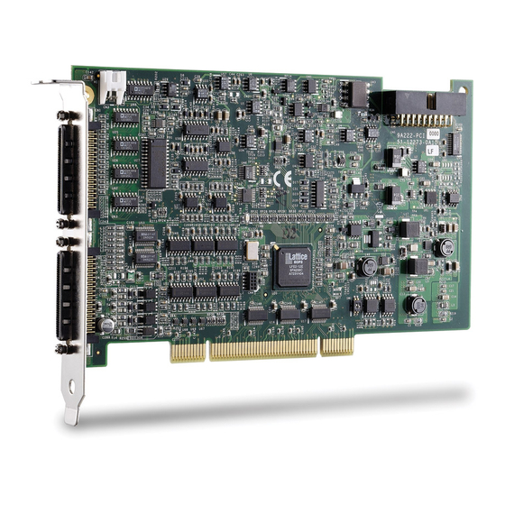
Summary of Contents for ADLINK Technology NuDAQ PCI-9222
- Page 1 ® NuDAQ PCI-9222 ® NuDAQ PCI-9223 16-bit High-Performance DAQ Card with Programmable Function I/O User’s Manual Manual Rev. 2.00 Revision Date: April 24, 2008 Part No: 50-11237-1000 Advance Technologies; Automate the World.
- Page 2 Copyright 2008 ADLINK TECHNOLOGY INC. All Rights Reserved. The information in this document is subject to change without prior notice in order to improve reliability, design, and function and does not represent a commitment on the part of the manufacturer.
- Page 3 Sales & Service info@adlinktech.com Toll-Free +1-866-4-ADLINK (235465) Fax No. +1-949-727-2099 Mailing Address 8900 Research Drive, Irvine, CA 92618, USA ADLINK TECHNOLOGY EUROPEAN SALES OFFICE Sales & Service emea@adlinktech.com Toll-Free +49-211-4955552 Fax No. +49-211-4955557 Mailing Address Nord Carree 3, 40477 Düsseldorf, Germany ADLINK TECHNOLOGY SINGAPORE PTE LTD Sales &...
- Page 4 ADLINK TECHNOLOGY KOREA Sales & Service korea@adlinktech.com Telephone No. +82-2-20570565 Fax No. +82-2-20570563 Mailing Address #402, Dongsung B/D, 60-12, Nonhyeon-Dong Gangnam-gu, Seoul, 135-010, South Korea ADLINK TECHNOLOGY BEIJING Sales & Service market@adlinkchina.com.cn Telephone No. +86-10-5885-8666 Fax No. +86-10-5885-8625 Mailing Address Room 801, Building E, Yingchuangdongli Plaza, No.1 Shangdidonglu,...
- Page 5 1.2 How this manual is organized This manual is organized as follows: Chapter 1 Introduction: This chapter introduces the ADLINK NuDAQ PCI-9222 and NuDAQ PCI-9223 cards including their features, specifications, software support information, and package contents. Chapter 2 Hardware Information: This chapter presents the card’s layout, connector pin assignment, signal descriptions,...
- Page 6 1.3 Conventions Take note of the following conventions used throughout the man- ual to make sure that you perform certain tasks and instructions properly. NOTE Additional information, aids, and tips that help you per- form particular tasks. IMPORTANT Critical information and instructions that you MUST perform to complete a task.
-
Page 7: Table Of Contents
Table of Contents List of Tables................iii List of Figures ................ iv 1 Introduction ................ 1 Features................2 Applications ................. 2 Specifications............... 3 Unpacking Checklist ............8 Software Support ..............8 Driver Support for Windows ..........9 2 Hardware Information ............13 Card Layout ............... - Page 8 Trigger Modes ............... 33 Bus-mastering DMA Data Transfer ....... 35 D/A Conversion..............38 Bipolar Output Modes ........... 38 Software Update ............38 Waveform Generation ........... 38 Programmable Function I/O..........47 TTL DI/DO ..............47 General Purpose Timer/Counter ........48 Basic Timer/Counter Functions ........48 General Purpose Timer/Counter Modes .......
-
Page 9: List Of Tables
List of Tables Table 2-1: CN1 Pin Assignment for PCI-9222 ......14 Table 2-2: CN1 Pin Assignment for PCI-9223 ......15 Table 2-3: CN2 Pin Assignment for PCI-9222/PCI-9223 ..16 Table 2-4: CN1/CN2 Signal Description ........17 Table 2-5: SSI Connector Pin Assignment ......18 Table 2-6: SSI Connector Signal Description ...... - Page 10 List of Figures Figure 1-1: ADLINK Software Support Overview ......9 Figure 1-2: DAQPilot Main Interface ..........9 Figure 1-3: DAQMaster Device Manager........10 Figure 1-4: Legacy Software Support Overview ......11 Figure 2-1: PCI-9222/PCI-9223 Layout........13 Figure 2-2: Floating Source and RSE Input Connections ..21 Figure 2-3: Ground-referenced Sources and NRSE Input Connections.........
- Page 11 Figure 4-26: Mode 9 Operation............ 54 Figure 4-27: Mode 10 Operation..........54 Figure 4-28: Digital Waveform Acquisition Operation ....55 Figure 4-29: Digital Waveform Generation Operation....56 Figure 4-30: Encoder Isolation Input Module ....... 57 Figure 4-31: Encoder OGRx Input ..........58 Figure 4-32: CW/CCW Encoder Timing........
-
Page 13: Introduction
Introduction The NuDAQ PCI-9222 (16-CH, 250 kS/s) and NuDAQ PCI-9223 (32-CH, 500 kS/s) are 16-bit high-performance DAQ cards with eight different input ranges. These cards also features a 2-CH, 16- bit analog output capable of up to 1 MS/s update rate, a 2-CH encoder input, and a programmable function I/O. -
Page 14: Features
1.1 Features The PCI-9222/PCI-9223 comes with the following features: Supports a 32-bit 3.3 V or 5 V PCI bus PCI 2.3-compliant Up to 32-CH single-ended or 16-CH differential analog input Up to 500 kS/s sampling rate Programmable analog input gains of 1, 2, 4, 5, 8, 10, 20, 40 2-CH, 16-bit simultaneous analog output supports update rate of up to 1 MS/s Programmable function I/O supports the following modes:... -
Page 15: Specifications
1.3 Specifications Analog Input (AI) Hardware PCI-9222 PCI-9223 Number of channels (programmable) A/D converter AD7685 or equivalent AD7686 or equivalent Maximum sampling rate Single-channel: 250 K samples/s 500 K samples/s Scanning: 100 K samples/s 200 K samples/s Resolution 16-bit Input coupling Programmable input range ±10 V, ±5 V, ±2.5 V, ±2 V, ±1.25 V, ±1 V, ±500 mV, ±250 mV... - Page 16 Spurious-free dynamic range 95 dB 88 dB (SFDR) Signal-to-noise and distortion 86 dB 84 dB ratio (SINAD) Total harmonic distortion –94 dB –90 dB (THD) Signal-to-noise ration (SNR) 87 dB 86 dB Effective number of bits 13.9 13.5 (ENOB) Settling time to full-scale step Multiple channels 2 µs to 0.1% error Multiple ranges...
- Page 17 Fall time 0.7 µs Settling time to 1% output 3 µs error 0.7 LSB 1 LSB Output driving ±5 mA (maximum) Function I/O Number of channels • 16-CH programmable function DI • 16-CH programmable function DO Compatibility TTL (single-ended) (supports 3.3 V and 5 V DI; 3.3 V DO) Input voltage •...
- Page 18 Encoder Input (EI) Number of channels Max. Input frequency 4 MHz Encoder count (2³¹-1) bits Photo isolator NEC PS9115 or equivalent Encoder modes • CW/CCW • X1 AB phase encoder • X2 AB phase encoder • X4 AB phase encoder Physical, Power, and Operating Environment Interface PCI 2.3-compliant...
- Page 19 2. System Noise (LSBrms, including Quantization, Typical, 25 º Input Range System Noise ±10 V 0.78 LSBrms ±5 V 0.80 LSBrms 0.98 LSBrms ±2.5 V ±2 V 0.96 LSBrms ±1.25 V 0.77 LSBrms ±1 V 0.81 LSBrms ±500 mV 0.99 LSBrms ±250 mV 0.96 LSBrms 3.
-
Page 20: Unpacking Checklist
1.4 Unpacking Checklist Before unpacking, check the shipping carton for any damage. If the shipping carton and/or contents are damaged, inform your dealer immediately. Retain the shipping carton and packing mate- rials for inspection. Obtain authorization from your dealer before returning any product to ADLINK. -
Page 21: Driver Support For Windows
Figure 1-1: ADLINK Software Support Overview Driver Support for Windows DAQPilot DAQPilot is a driver and SDK with a graphics-driven interface for various application development environments. DAQPilot comes as ADLINK's commitment to provide full support to its comprehensive line of data acquisition products and is designed for the novice to the most experienced programmer. -
Page 22: Figure 1-3: Daqmaster Device Manager
As a task-oriented DAQ driver, SDK and wizard for Windows systems, DAQPilot helps you shorten the development time while accelerating your learning curve for data acquisition pro- gramming. You can download and install DAQPilot at http://www.adlinktech.com/TM/DAQPilot.html DAQMaster The ADLINK DAQMaster is a smart device manager that opens up access to ADLINK data acquisition and test and mea- surement products. -
Page 23: Figure 1-4: Legacy Software Support Overview
PCIS-DASK (Legacy Drivers and Support) PCIS-DASK is composed of advanced 32-bit kernel drivers for customized application development. PCIS-DASK enables you to perform detailed operations and achieve supe- rior performance and reliability from your data acquisition sys- tem. DASK kernel drivers now support the revolutionary ®... - Page 24 PCIS-DASK drivers prepare legacy Windows users for Windows Vista and 64-bit editions of Windows. PCIS-DASK comes with the following features: Supports Windows Vista 32-bit or 64-bit editions Supports AMD64 and Intel x86-64 architectures Digitally-signed for Windows Vista 64-bit edition Utilizes WOW64 subsystem to ensure that 32-bit applications run normally on 64-bit editions of Windows XP, Windows 2003 Server, and Windows Vista without modification...
-
Page 25: Hardware Information
Hardware Information This chapter provides information on the PCI-9222/PCI-9223 lay- out, connectors, and pin assignments. 2.1 Card Layout Figure 2-1 shows the PCI-9222/PCI-9223 board layout and dimen- sions. 102.46 70.22 106.4 Figure 2-1: PCI-9222/PCI-9223 Layout 2.2 Connector Pin Assignment The PCI-9222/PCI-9223 card is equipped with two VHDCI 68-pin connectors. -
Page 26: Cn1 Pin Assignment
CN1 Pin Assignment Definition Pin # Definition AI0(AIH0) AI8(AIL0) AI1(AIH1) AI9(AIL1) AI2(AIH2) AI10(AIL2) AI3(AIH3) AI11(AIL3) AI4(AIH4) AI12(AIL4) AI5(AIH5) AI13(AIL5) AI6(AIH6) AI14(AIL6) AI7(AIH7) AI15(AIL7) AGND AISENSE AGND AGND AGND AGND Table 2-1: CN1 Pin Assignment for PCI-9222 Hardware Information... -
Page 27: Table 2-2: Cn1 Pin Assignment For Pci-9223
Definition Pin # Definition AI0(AIH0) AI16(AIL0) AI1(AIH1) AI17(AIL1) AI2(AIH2) AI18(AIL2) AI3(AIH3) AI19(AIL3) AI4(AIH4) AI20(AIL4) AI5(AIH5) AI21(AIL5) AI6(AIH6) AI22(AIL6) AI7(AIH7) AI23(AIL7) AGND AISENSE AI8(AIH8) AI24(AIL8) AI9(AIH9) AI25(AIL9) AI10(AIH10) AI26(AIL10) AI11(AIH11) AI27(AIL11) AI12(AIH12) AI28(AIL12) AI13(AIH13) AI29(AIL13) AI14(AIH14) AI30(AIL14) AI15(AIH15) AI31(AIL15) AGND AGND AGND AGND Table 2-2: CN1 Pin Assignment for PCI-9223... -
Page 28: Cn2 Pin Assignment
CN2 Pin Assignment Definition Pin # Definition GPI0/GPTC_CLK0 GPI8/GPTC_CLK2 GPI1/GPTC_UD0 GPI9/GPTC_UD2 GPI2/GPTC_GATE0 GPI10/GPTC_GATE2 GPI3/GPTC_AUX0 GPI11/GPTC_AUX2 GPI4/GPTC_CLK1 GPI12/GPTC_CLK3 GPI5/GPTC_UD1 GPI13/GPTC_UD3 GPI6/GPTC_GATE1 GPI14/GPTC_GATE3 GPI7/GPTC_AUX1 GPI15/GPTC_AUX3 DGND DGND GPO0/GPTC_OUT0 GPO8 GPO1/GPTC_OUT1 GPO9 GPO2/GPTC_OUT2 GPO10 GPO3/GPTC_OUT3 GPO11 GPO4 GPO12 GPO5 GPO13 GPO6 GPO14 GPO7 GPO15 DGND DGND... -
Page 29: Cn1/Cn2 Signal Descriptions
CN1/CN2 Signal Descriptions Below are the signal descriptions for the CN1/CN2 connectors: Signal Name Reference Direction Description AIGND — — Analog input ground. All three ground references (AIGND, AOGND, and DGND) are connected onboard. AI<0..15> (16-CH) AIGND Input PCI-9222 Analog Input Channels 0~15. -
Page 30: Ssi Connector Pin Assignment
Signal Name Reference Direction Description EZ<0, 1> Encoder Input Encoder Z Phase Ground ORG<0, 1> Encoder Input Encoder Original Signal Ground Encoder +24V Encoder Input Encoder voltage input pin Ground GPTC_CLK<0, 3> DGND Input GPTC<0, 3> clock source GPTC_GATE<0, 3> DGND Input GPTC<0, 3>... -
Page 31: Ssi Connector Signal Description
SSI Connector Signal Description Signal Name Setting Direction Description SSI_ADCONV Master Output Sends out the ADCONV Slave Input Accepts the SSI_ADCONV to replace the internal ADCONV signal SSI_AD_TRIG Master Output Sends the internal AD_TRIG out Slave Input Accepts the SSI_AD_TRIG as the digital trigger signal SSI_DAWR Master... -
Page 32: Analog Input Signal Connection
2.3 Analog Input Signal Connection The PCI-9222 provides up to 16 single-ended or 8 differential ana- log input channels, while the PCI-9223 offers up to 32 single- ended or 16 differential analog input channels. You can fill the Channel Gain Queue to get the desired input signal type combina- tion. -
Page 33: Input Configurations
Input Configurations Single-ended Connections A single-ended connection is used when the analog input sig- nal is referenced to a ground that can be shared with other analog input signals. There are two types of single-ended con- nections: RSE and NRSE configuration. In RSE configuration, the PCI-9222/PCI-9223 card provides the grounding point for external analog input signals and is suitable for floating signal sources. -
Page 34: Figure 2-3: Ground-Referenced Sources And Nrse Input Connections
Non-Referenced Single-Ended (NRSE) Mode To measure ground-referenced signal sources, which are con- nected to the same ground point, you can connect the signals in NRSE mode. Figure 2-3 illustrates the connection. The sig- nal’s local ground reference is connected to the negative input of the instrumentation amplifier (AISENSE pin on CN1 connec- tor), and the common-mode ground potential between signal ground and the onboard ground will be rejected by the instru-... -
Page 35: Figure 2-5: Floating Source And Differential Input
Figure 2-5 shows how to connect a floating signal source to the PCI-9222/PCI-9223 card in differential input mode. For floating signal sources, you need to add a resistor at each channel to provide a bias return path. The resistor value should be about 100 times the equivalent source impedance. - Page 36 Hardware Information...
-
Page 37: Installation
Installation 3.1 Before You Proceed The PCI-9222/PCI-9223 card has electro-static sensitive compo- nents that can be easily damaged by static electricity. The card must be handled on a grounded anti-static mat. The operator must wear an anti-static wristband, grounded at the same point as the anti-static mat. -
Page 38: Configuring The Card
6. Replace the system/chassis cover. 7. Connect the power plug to a power source, then turn on the system. 3.3 Configuring the Card As a plug and play component, the card requests an interrupt number through its PCI controller. The system BIOS responds with an interrupt assignment based on the card information and on known system parameters. -
Page 39: Operation Theory
Operation Theory The operation theory of each function in the PCI-9222/PCI-9223 card is described in this chapter. These functions include A/D conversion, D/A conversion, encoder, programmable function I/O, and more. The operation theory can help you understand how to configure and program the PCI-9222/PCI-9223 card. 4.1 Block Diagram There are 32/16 single-ended channels of 16-bit A/D input and 2 single-ended channels of 16-bit D/A output available in the PCI-... -
Page 40: A/D Conversion
4.2 A/D Conversion When using an A/D converter, you must know about the properties of the signal to be measured and decide which channel to use and how to connect the signals to the card. Refer to section 2.3. In addition, you should define and control the A/D signal configurations, including channels, gains, and signal types. -
Page 41: Ai Data Format
AI Data Format The data format of the acquired 16-bit A/D data is 2’s complement coding. Table 4-1 shows the valid input ranges and the ideal transfer characteristics. Digital Description Bipolar Analog Input Range code Full-scale Range ±10V ±5V ±2.5V ±2V Least significant bit 305.2uV... -
Page 42: Continuous Acquisition (Scanning) Mode
This method is suitable for applications that need to process A/D data in real time. In this mode, the timing of the A/D conversion is fully controlled by the software. The A/D conversion rate is decided by the software timer and may not be totally precise. In Software Polling, the channel, gain, and input configuration (RSE, NRSE, or DIFF) may be specified for each single-point measurement. -
Page 43: Figure 4-4: Scan Timing
SI_counter (32-bit) Specify the Scan Interval = SI_counter / Timebase SI2_counter (24-bit) Specify the Data Sampling Interval = SI2_counter/Timebase PSC_counter (31-bit) Specify the Post Scan Counts after a trigger event NumChan_counter (8-bit) Specify the number of samples per scan The acquisition timing and the meaning of the four counters are illustrated in Figure 4-4. - Page 44 NOTES • The maximum A/D sampling rate is 250 kHz for PCI-9222 and 500 kHz for PCI-9223. The minimum setting for the SI2_counter when using the internal Timebase is 320 (PCI-9222) and 160 (PCI-9223). • The SI_counter is 32-bit while the SI2_counter is 24-bit. The maxi- mum scan interval using the internal Timebase = 2 /80 Ms = 53.687s, and the maximum sampling interval between two chan-...
-
Page 45: Trigger Modes
Trigger Modes The PCI-9222/PCI-9223 supports two trigger sources: internal software and external digital trigger. You must select one as the trigger event source. A trigger event occurs when the specified condition is detected on the selected trigger source. For example, a rising edge on the external digital trigger input. -
Page 46: Figure 4-6: Post Trigger With Retrigger
Use Retrig_no to specify the re-trigger numbers. In Figure 4-6, two scans of data are acquired after the first trigger signal, then the card waits for the retrigger signal (retrigger signals which occur before the scans are completed will be ignored). When the retrigger signal occurs, two more scans are performed. -
Page 47: Bus-Mastering Dma Data Transfer
total acquired data length NumChan_counter *PSC_counter. Figure 4-7: Gated Trigger with Finite Scan Acquisition Bus-mastering DMA Data Transfer In programmable scan acquisition mode, the PCI-9222/PCI-9223 supports bus-mastering DMA data transfer. PCI bus-mastering DMA is necessary for high speed DAQ in order to utilize the maximum PCI bandwidth. -
Page 48: Figure 4-8: Scatter-Gather Dma For Data Transfer
simply need to assign the sampling period and the number of conversion through their specified counters. After the AD trigger condition is matched, the data will be transferred to the system memory by the bus-mastering DMA. The PCI controller also supports the scatter/gather bus mastering DMA function that enables transfer of large amounts of data by linking all the memory blocks into a continuous linked list. - Page 49 In non-chaining mode, the maximum DMA data transfer size is 2M double words (8 MB). However, by using chaining mode-scatter/ gather, there is no limitation for the DMA data transfer size. You may also link the descriptor nodes circularly to achieve a multi- buffered mode DMA.
-
Page 50: D/A Conversion
4.3 D/A Conversion For complex applications, the PCI-9222/PCI-9223 offers software polling to update the output, and DMA data transfer to generate waveform. This means that the D/A update rate is not only controlled by software timing, but can also be set by a precision hardware timer that you specified. -
Page 51: Figure 4-9: Fifo Data In/Out Structure
Waveform patterns larger than 512 samples are also supported using bus-mastering DMA transfer via the PCI controller. Data format in FIFO is shown in Figure 4-9. Figure 4-9: FIFO Data In/Out Structure DMA transfers data according to channel order. Figure 4-10 shows DA channel 0 to channel 3 data, while channel 2 is disabled. -
Page 52: Table 4-4: Summary Of Counters For Waveform Generation
You can choose the update clock source by setting the AO source configuration. Refer to Figure 4-11. It is recommended that you use the internal hardware to get a more precise update rate. Internal Timer AO update clock GPI[7..0] Figure 4-11: Waveform Generation Clock Source Selection Waveform Generation with Internal Hardware Timer Six counters interact with the waveform to generate different DAWR timing to form various waveforms. -
Page 53: Figure 4-12: Typical D/A Timing Of Waveform Generation
DLY2_counter 32-bit Defines the delay time Delay Time = to separate consecutive (DLY2_counter / Clock waveform generation. Timebase) This is applicable only in Iterative Waveform Generation mode. Trig_counter 32-bit Defines the acceptable start trigger count when re-trigger function is enabled Table 4-4: Summary of Counters for Waveform Generation Timebase*= 80M NOTE... -
Page 54: Figure 4-13: Post-Trigger Generation
Trigger Modes Post-Trigger Generation Use post-trigger generation when you want to generate a waveform right after a trigger signal. The number of patterns to be updated after the trigger signal is specified by UC_counter* IC_counter and is illustrated in Figure 4-13. Figure 4-13: Post-Trigger Generation Delay-Trigger Generation Use delay-trigger when you want to delay the waveform... -
Page 55: Figure 4-14: Delay-Trigger Generation
Figure 4-14: Delay-Trigger Generation Post-Trigger or Delay-Trigger with Retrigger Use post-trigger or delay-trigger with retrigger when you want to generate multiple waveforms with respect to multiple incoming trigger signals. You can set Trig_counter to specify the number of acceptable trigger signals. Refer to Figure 4-15. In this example, two waveforms are generated after the first trigger signal. -
Page 56: Figure 4-15: Post-Trigger With Retrigger Generation
Figure 4-15: Post-Trigger with Retrigger Generation NOTE Start Trigger signals asserted during the waveform gen- eration process will be ignored. Iterative Waveform Generation You can set the IC_counter to generate iterative waveforms regardless of the trigger mode used. The IC_counter stores the iteration number. -
Page 57: Figure 4-16: Finite Iterative Waveform Generation With
If the value specified in UC_counter is smaller than the sample size of the waveform patterns, the waveform will be generated piece-wisely. For example, if you defined a 16-sample sine wave and set the UC_counter to 2, the generated waveform will be a 1/8-cycle sine wave for every waveform period, and a complete sine wave will be generated for every 8-iterations. -
Page 58: Figure 4-17: Infinite Iterative Waveform Generation With
Figure 4-17: Infinite Iterative Waveform Generation with Post-trigger In conjunction with different trigger modes and counter setups, you can manipulate a single waveform to generate different and more complex waveforms. DLY2_Counter in Iterative Waveform Generation To expand the flexibility of iterative waveform generation, DLY2_counter was implemented to separate consecutive waveform generations. -
Page 59: Programmable Function I/O
4.4 Programmable Function I/O The PCI-9222/PCI-9223 supports a powerful programmable function I/O provided by an FPGA chip. These function I/O can be configured as TTL DI/DO or 32-bit timer/counters. In addition, the timer/counter supports a variety of modes, including general purpose timer/counter, PWM output, or encoder input for simple motion control. -
Page 60: General Purpose Timer/Counter
General Purpose Timer/Counter The PCI-9222/PCI-9223 comes with three general purpose timer/ counter sets featuring: Count up/down controlled by hardware or software Programmable counter clock source (internal clock up to 80 MHz, external clock up to 10 MHz) Programmable gate selection (hardware or software control) Programmable input and output signal polarities (high active or low active) Initial Count can be loaded from a software application... -
Page 61: General Purpose Timer/Counter Modes
controls the counter to count up or down (high: count up; low: count down), while the GPTC_GATE input is a control signal which acts as a counter enable or a counter trigger signal under different applications. The GPTC_OUT will then generate a pulse signal based on which timer/counter mode you have set. -
Page 62: Figure 4-19: Mode 2 Operation
Mode 2: Single Period Measurement The counter counts the period of the signal on GPTC_GATE in terms of GPTC_CLK. Initial count can be loaded from the software application. After the software-start, the counter counts the number of active edges on GPTC_CLK between two active edges of GPTC_GATE. -
Page 63: Figure 4-20: Mode 3 Operation
Figure 4-20: Mode 3 Operation Mode 4: Single Gated Pulse Generation This generates a single pulse with programmable delay and programmable pulse-width following the software-start. The two programmable parameters can be specified in terms of periods of the GPTC_CLK input by the software application. GPTC_GATE is use to enable/disable counting. -
Page 64: Figure 4-22: Mode 5 Operation
Mode 5: Single Triggered Pulse Generation This mode generates a single pulse with programmable delay programmable pulse-width following active GPTC_GATE edge. You may specify these programmable parameters in terms of periods of the GPTC_CLK input. When the first GPTC_GATE edge triggers the single pulse, GPTC_GATE makes no effect until the software-start is executed again. -
Page 65: Figure 4-24: Mode 7 Operation
Mode 7: Single Triggered Continuous Pulse Generation This mode is similar to Mode 5 except that the counter generates continuous periodic pulses with programmable pulse interval and pulse-width following the first active edge of GPTC_GATE. When the first GPTC_GATE edge triggers the counter, GPTC_GATE makes no effect until the software-start is executed again. -
Page 66: Figure 4-26: Mode 9 Operation
Mode 9: Edge Separation Measurement Measures the time differentiation between two different pulse signals. The first pulse signal is connected to GPTC_GATE and the second signal is connected to GPTC_AUX. It counts the clocks that pass by between the rising edge signal of two different pulses through the 40MHz internal clock or external clock. -
Page 67: Digital Waveform Acquisition And Generation
Digital Waveform Acquisition and Generation The PCI-9222/PCI-9223 GPI and GPO support digital waveform generation and digital waveform acquisition. You can sample GPI or update GPO based on the precision hardware timer. Digital Waveform Acquisition The digital data on GPI channels can be acquired by using the digital waveform acquisition mode. -
Page 68: Figure 4-29: Digital Waveform Generation Operation
Digital Waveform Generation The digital output on GPO [15..0] channels can be updated by using digital waveform generation mode. This works similar to AO waveform generation. With periodic update clock, you can generate a sequence of digital output patterns based on precision hardware time interval. -
Page 69: Isolation Encoder
4.5 Isolation Encoder PCI-9222/PCI-9223 features combination data acquisition and simple motion control with support for two channel encoder input sets which provide an alternative for step motor or servo motor's position feedback. The encoder sets are assigned in CN2. Definition Pin # Definition E24V... -
Page 70: Figure 4-31: Encoder Ogrx Input
The Encoder OGRx input is different from the encoder phase input since you need to add an external +24V power to drive the photo-couple. Figure 4-31 shows the OGRx input. Figure 4-31: Encoder OGRx Input CW/CCW Encoder Mode When GPTC is set to CW/CCW encoder mode and when the input EAx is connected to CW source signal and EBx is connected to CCW source signal, pulses from EAx will cause the counter to counter up and spin the motor clockwise. -
Page 71: Figure 4-33: X1 Encoder Mode
X1 Encoder Mode In X1 encoder mode, if phase A (EA0/EA1) is advanced of phase B (EB0/EB1) in a quadrature cycle, the increment of counter value will be 1. Otherwise, if phase B is advanced of phase A in a quadrature cycle, the decrement of counter value will also be 1. -
Page 72: Figure 4-35: X4 Encoder Mode
X4 Encoder Mode This mode is similar to X1 Encoder Mode, except that the amount of counter value increases or decreases by four. Refer to Figure 4-35. Figure 4-35: X4 Encoder Mode Phase Z Each encoder mode may use a third phase, phase Z, that is also frequently used for the index phase. -
Page 73: Figure 4-36: Phase Z
Figure 4-36: Phase Z Original Signal (ORGx) Original Signal (ORG0/ORG2/ORG1) is used with phase Z. With ORG enabled, a high level on phase Z and ORG causes the counter to reload with a specified value in a specified phase of the quadrature cycle. When you use ORG signal if it is at a low level and phase Z is at a high level, then counter reload is ignored. -
Page 74: Trigger Sources
4.6 Trigger Sources The PCI-9222/PCI-9223 supports two trigger sources for analog input, analog output, and digital waveform acquisition/generation: software trigger and external digital trigger. Software Trigger This trigger mode does not need any external trigger source. The trigger asserts right after you execute the specified function calls to begin data acquisition. -
Page 75: Calibration
Calibration This chapter introduces the card calibration process to minimize AD measurement errors and DA output errors. 5.1 Loading Calibration Constants The PCI-9222/PCI-9223 is factory-calibrated before shipment. The associated calibration constants of the TrimDACs firmware are written to the onboard EEPROM. TrimDACs firmware is the algorithm in the FPGA. -
Page 76: Saving Calibration Constants
5.3 Saving Calibration Constants Factory-calibrated constants are permanently stored in a bank of the onboard EEPROM and may not be modified. When you re-cal- ibrate the device, the software stores the new constants in a user- configurable section of the EEPROM. To return a device to its ini- tial factory calibration settings, the software can copy the factory calibrated constants to the user-configurable section of the EEPROM. -
Page 77: Warranty Policy
Warranty Policy Thank you for choosing ADLINK. To understand your rights and enjoy all the after-sales services we offer, please read the follow- ing carefully. 1. Before using ADLINK’s products please read the user man- ual and follow the instructions exactly. When sending in damaged products for repair, please attach an RMA appli- cation form which can be downloaded from: http:// rma.adlinktech.com/policy/. - Page 78 3. Our repair service is not covered by ADLINK's guarantee in the following situations: Damage caused by not following instructions in the User's Manual. Damage caused by carelessness on the user's part dur- ing product transportation. Damage caused by fire, earthquakes, floods, lightening, pollution, other acts of God, and/or incorrect usage of voltage transformers.
Need help?
Do you have a question about the NuDAQ PCI-9222 and is the answer not in the manual?
Questions and answers