Table of Contents
Advertisement
Quick Links
LM48511 Evaluation Board
User's Guide
Quick Start Guide
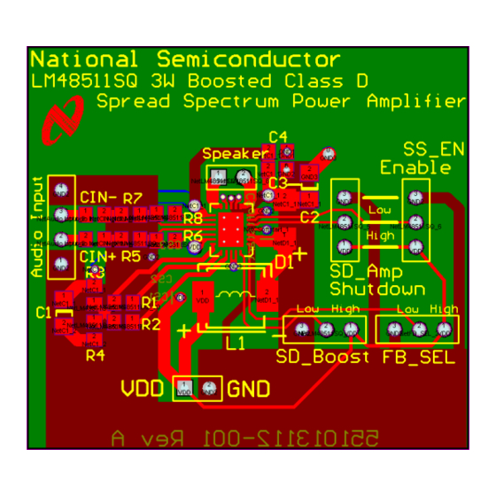
Apply a 3.0V to 5.5V power supply voltage to the VDD pin with
respect to the ground (GND) pin.
Set connectors SD_Amp, SS_En Enable, SD_Boost to High.
Set FB_SEL to Low (FB_SEL0) which boosts the regulator
output voltage PV1 to about 7.6V.
Apply a mono differential input signal into the Audio Input's
two center pins of the 4-pin connector.
Apply power. Make measurements.
© 2008 National Semiconductor Corporation
FIGURE 1. Typical LM48511SQ Demonstration Board
300855
National Semiconductor
Application Note 1922
Allan Soriano
November 5, 2008
Introduction
To help the user investigate and evaluate the LM48511SQ
performance and capabilities, a fully populated demonstration
board was created. Please contact National Semiconductor
Corporation's Audio Products Group for availability. This
board is shown in Figure 1. Connected to an external power
≤
≤
supply (3.0V
VDD
LM48511SQ demonstration board easily exercises the
amplifier's features.
5.5V) and a signal source, the
30085503
www.national.com
Advertisement
Table of Contents

Subscribe to Our Youtube Channel
Related Manuals for National Semiconductor LM48511


Summary of Contents for National Semiconductor LM48511
- Page 1 To help the user investigate and evaluate the LM48511SQ respect to the ground (GND) pin. performance and capabilities, a fully populated demonstration board was created. Please contact National Semiconductor Set connectors SD_Amp, SS_En Enable, SD_Boost to High. Corporation’s Audio Products Group for availability. This Set FB_SEL to Low (FB_SEL0) which boosts the regulator board is shown in Figure 1.
-
Page 2: General Description
■ ≤ ≤ power supply. When operating from a 3V to 4V power supply, Supply Voltage (V 3.0V ±5.5V the LM48511 can be configured to drive 1 to 2.5W into an ■ ≤ ≤ Amplifier Voltage (PV1, V1) 4.8V ±8.0V 8Ω... - Page 3 Schematic 30085504 FIGURE 2. Typical LM48511 Audio Amplifier Application Circuit www.national.com...
-
Page 4: Pcb Layout Guidelines
The two center pins of the 4 pin connector on the left above are used as differential inputs into the Audio Input LM48511, or two single-ended inputs when one center pin and an outer ground pin are paired. Speaker (Audio Output) The differential output for an 8Ω... -
Page 5: Bill Of Materials
Bill Of Materials Designator Description Footprint Quantity Value CHIP CAPACITOR GENERIC CAP 0805 470pF 1μF CINA CHIP CAPACITOR GENERIC CAP 1210 1μF CHIP CAPACITOR GENERIC CINB CAP 1210 10μF CHIP CAPACITOR GENERIC CAP 1210 2.2μF CHIP CAPACITOR GENERIC CAP 1210 4.7μF CHIP CAPACITOR GENERIC CAP 1210... - Page 6 surface. Figure 4 is the metal Top Layer. Figure 5 is the metal Demonstration Board PCB Layout Midlayer 1. Figure 6 is the metal Midlayer 2. Figure 7 is the Figures 3 through 8 shows the different layers used to create metal Bottom Layer.
- Page 7 30085505 FIGURE 5. Mid Layer 1 30085506 FIGURE 6. Mid Layer 2 www.national.com...
- Page 8 30085501 FIGURE 7. Bottom Layer 30085502 FIGURE 8. Bottom Overlay www.national.com...
-
Page 9: Typical Performance Characteristics
Typical Performance Characteristics THD+N vs Frequency THD+N vs Frequency = 8Ω = 8Ω = 5V, R = 3.6V, R = 2W, filter = 22kHz, PV = 7.8V = 500mW, filter = 22kHz, PV = 4.8V 30085519 30085518 THD+N vs Frequency THD+N vs Output Power = 8Ω... - Page 10 THD+N vs Output Power THD+N vs Output Power = 8Ω = 8Ω = 3V, 3.6V, 5V, R = 3.6V, R filter = 22kHz, PV = 7.8V, PV = 7V, PV = 4.8V, FF f = 1kHz, filter = 22kHz, R = 4.87kΩ, FF 30085525 30085524...
- Page 11 PSRR vs Frequency PSRR vs Frequency = 8Ω = 8Ω = 3.6V, R = 3V, R = 200mV , PV = 7V = 200mV , PV = 4.8V RIPPLE RIPPLE 30085530 30085531 Supply Current vs Supply Voltage Supply Current vs Supply Voltage = 7.8V = 7V 30085533...
- Page 12 Power Dissipation vs Output Power Power Dissipation vs Output Power = 8Ω = 8Ω = 3.6V, R = 3V, R = 7V, FF = 4.8V, FF 30085536 30085537 Boost Converter Efficiency vs I Boost Converter Efficiency vs I LOAD(DC) LOAD(DC) = 5V, PV = 7.8V = 3.6V, PV...
-
Page 13: Revision History
Revision History Date Description 11/05/08 Initial release. www.national.com... - Page 14 Notes For more National Semiconductor product information and proven design tools, visit the following Web sites at: Products Design Support Amplifiers www.national.com/amplifiers WEBENCH® Tools www.national.com/webench Audio www.national.com/audio App Notes www.national.com/appnotes Clock and Timing www.national.com/timing Reference Designs www.national.com/refdesigns Data Converters www.national.com/adc Samples www.national.com/samples...
Need help?
Do you have a question about the LM48511 and is the answer not in the manual?
Questions and answers