Table of Contents
Advertisement
Quick Links
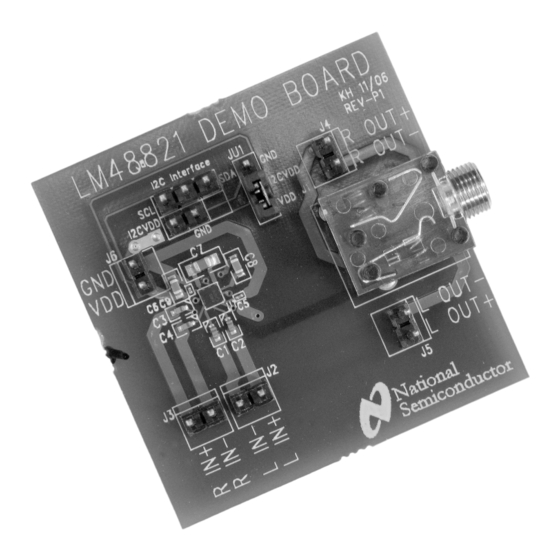
LM48821 Evaluation Board
User's Guide
Quick Start Guide
Connect the I
2
C signal generation and interface board to a
computer's parallel port.
Install LM48821 control software: "LM48821_Software."
Amplifier output mode:
Apply a 2.0V to 4.0V power supply's positive voltage output
to the "VDD" pin on jumper J6. Apply the power supply's
ground return to the "GND" pin on J6.
Connect the supplied 5-wire cable between the I
generation and interface board and the 5-pin connector (I2C
Interface) on the LM48821 demonstration board.
Apply a stereo audio signal to jumpers JP2(Left) and JP3
(Right). Apply the source's +input and -input to the "+" pin and
the "-" pin, respectively.
≥
16Ω) to JP(Right) and another load to JP5
Connect a load (
(Left). JP4's "+" pin and JP's "+" pin carries the output signals
© 2007 National Semiconductor Corporation
2
C signal
FIGURE 1. The LM48821 Demonstration Board
300098
National Semiconductor
Application Note 1589
Kevin Hoskins
May 2007
from the two amplifiers found on pins OUTR and OUTL, re-
spectively.
Apply power. Make measurements. Plug in a pair of head-
phones. Enjoy.
Introduction
To help the user investigate and evaluate the LM48821's per-
formance and capabilities, a fully populated demonstration
board is available from the National Semiconductor
Corporation's Audio Products Group. This board is shown in
Figure 1. Connected to an external power supply (2.0V to
4.0V), a signal source and an I
the LM48821 demonstration board easily demonstrate the
amplifier's features.
2
C controller (or signal source),
30009811
www.national.com
Advertisement
Table of Contents

Related Manuals for National Semiconductor LM48821


Summary of Contents for National Semiconductor LM48821
-
Page 1: Quick Start Guide
Amplifier output mode: Apply a 2.0V to 4.0V power supply’s positive voltage output To help the user investigate and evaluate the LM48821's per- to the “VDD” pin on jumper J6. Apply the power supply’s formance and capabilities, a fully populated demonstration ground return to the “GND“... -
Page 2: General Description
The LM48821 is a fully differential input stereo headphone Temperature Range –40°C 85°C audio amplifier with an internal digitally controlled volume ■ Amplifier Power control. The LM48821 is optimized to operate over a power ≤ ≤ ≤ 2.0V 5.0V 4.0V Supply Voltage supply voltage range of 2.0V to 4.0V. - Page 3 Connections Connecting to the world is accomplished through the 0.100” headers on the LM48821 demonstration board. The functions of the different headers are detailed in Table 1. TABLE 1. LM48821 Demonstration Board Connections Jumper Designation Function or Use Stereo, 0.125” headphone jack. Left channel is on the tip connector and the right channel is on the ring connector.
-
Page 4: Power Supply Sequencing
Setup will create a folder named set to minimum, and the mute function active. “LM48821” in the “Program” folder on the “C” disk (if the de- fault is used) along with a shortcut of the same name in the C Signal Generation Board and “Programs”... -
Page 5: Bill Of Materials
Bill of Materials Designator Part Description Value Tolerance Rating Package Manufacturer Manufacturer's Type Part Number TACmicrochip 0.47μF C1–C4 tantalum ±20% 0402 TACK474M010PTA capacitor Multilayer 0.1μF C5, C9 Ceramic ±10% 6.3V 0201 C0603X5R1A104M Capacitor Multilayer 4.7μF C6, C8 Ceramic ±20% 6.3V 0603 C1608X5R1A475M Capacitor... - Page 6 Figure 6 is the upper inner layer. Figure 7 is the lower middle Figures 4 through 9 show the different layers used to create layer. Figure 8 is the bottom layer. Figure 9 is the bottom the LM48821 four-layer demonstration board. Figure 4 is the silkscreen layer. 30009845 Figure 4.
- Page 7 30009843 Figure 7. Lower Middle Layer (Shown 2.6X actual size) 30009840 Figure 8. Bottom Layer (Shown 2.6X actual size) 30009841 Figure 9. Bottom Silk Layer (Shown 2.6X actual size) www.national.com...
-
Page 8: Typical Performance
Typical Performance Stereo THD+N vs Output Power Stereo THD+N vs Output Power = 16Ω, A = 16Ω, A = 0dB, f = 100Hz = 0dB, f = 1kHz at (from left to right at 1% THD+N): at (from left to right at 1% THD+N): = 2V, V = 3V, V = 4V,... - Page 9 Stereo THD+N vs Output Power Stereo THD+N vs Output Power = 32Ω, A = 32Ω, A = 0dB, f = 1kHz = 0dB, f = 10kHz at (from left to right at 1% THD+N): at (from left to right at 1% THD+N): = 2V, V = 3V, V = 4V,...
- Page 10 Appendix A LM48821 I C Control Register Table B1 shows the actions that are implemented by manipulating the bits within the internal I C control register. Table A1. LM48821 I C Control Register Addressing and Data Format Chart C Address...
- Page 11 ume control register in binary fashion increases the volume Appendix B Volume Control control setting, reaching full scale at 11111. Table B1 shows Settings Binary Values the value of the gain for each of the 32 binary volume control settings. The minimum volume setting is set to –76dB when 00000 is loaded into the volume control register.
- Page 12 Since National Semiconductor is constantly pursuing the best Appendix C Micro SMD Wafer Level package performance possible, please refer to the following Chip Scale Package, PCB, Layout, web page for possible updates to the μSMD package infor- mation presented in Appendix D: <http://www.national.com/ and Mounting Considerations an/AN/AN-1112.pdf.
-
Page 13: Revision History
Revision History Date Description 05/14/07 Initial release. www.national.com... - Page 14 National Semiconductor and the National Semiconductor logo are registered trademarks of National Semiconductor Corporation. All other brand or product names may be trademarks or registered trademarks of their respective holders.
Need help?
Do you have a question about the LM48821 and is the answer not in the manual?
Questions and answers