Table of Contents
Advertisement
Quick Links
GE
Intelligent Platforms
Installation Guide
VMIACC-7055*/ACC-7055RC*
CompactPCI
VMICPCI-7055*/CPCI-7055RC*
THE ACC-7055RC IS DESIGNED TO MEET THE EUROPEAN UNION (EU) RESTRICTION OF HAZARD-
OUS SUBSTANCE (ROHS) DIRECTIVE (2002/95/EC) CURRENT REVISION.
Publication No: 522-807055-000 Rev. D
®
Rear Transition Board for the
Advertisement
Table of Contents

Related Manuals for GE CompactPCI VMIACC-7055 Series


Summary of Contents for GE CompactPCI VMIACC-7055 Series
- Page 1 Intelligent Platforms Installation Guide VMIACC-7055*/ACC-7055RC* ® CompactPCI Rear Transition Board for the VMICPCI-7055*/CPCI-7055RC* THE ACC-7055RC IS DESIGNED TO MEET THE EUROPEAN UNION (EU) RESTRICTION OF HAZARD- OUS SUBSTANCE (ROHS) DIRECTIVE (2002/95/EC) CURRENT REVISION. Publication No: 522-807055-000 Rev. D...
- Page 2 February 22, 2010 Waste Electrical and Electronic Equipment (WEEE) Returns GE is registered with an approved Producer Compliance Scheme (PCS) and, subject to suitable contractual arrangements being in place, will ensure WEEE is processed in accordance with the requirements of the WEEE Directive.
-
Page 3: Table Of Contents
Table of Contents List of Figures ................. . 4 List of Tables . -
Page 4: List Of Figures
List of Figures Figure 1-1 VMIACC-7055/ACC-7055RC Rear Transition Board ..........7 Figure 1-2 Installation of the VMIACC-7055/ACC-7055RC RTMs with a VMICPCI-7055/CPCI-7055RC SBC . -
Page 5: List Of Tables
List of Tables Table 1-1 40-pin IDE Header Pinout ..............11 Table 1-2 PIM Site (J10) Connector Pinout . -
Page 6: Handling And Installation
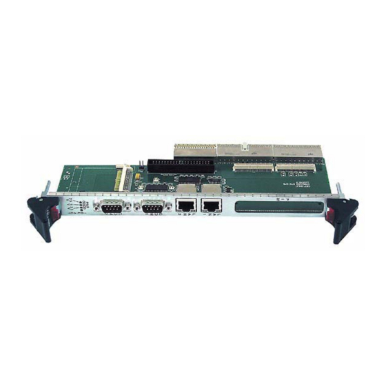
1 • Handling and Installation The VMIACC‐7055*/ACC‐7055RC* rear transition modules (RTMs) are designed to be used with the VMICPCI‐7055*/CPCI‐7055RC* single board computers (SBCs). The rear transition module is mounted in the rear I/O area of the chassis and provides associated signals from the front mounted SBC. The signals are routed to the backplane through the J3 and J5 connectors. The J4 connector is used for alignment only and has no electrical connections. The VMIACC‐7055/ACC‐7055RC boards are full 6U form factor boards with a CompactFlash connector, an internal IDE header, two COM ports, two LAN ports (option dependent), and one PIM site. Handling and Installation 6... -
Page 7: Figure 1-1 Vmiacc-7055/Acc-7055Rc Rear Transition Board
Figure 1-1 VMIACC-7055/ACC-7055RC Rear Transition Board VMIACC-7055/ ACC-7055RC PIM Site LAN 1 10/100/1000 Ethernet #1 10/100/1000 Ethernet #2 LAN 2 COM 1 RS232 or RS422/485 #1 RS232 or RS422/485 #2 COM 2 CompactFlash LEDs Handling and Installation 7... -
Page 8: Installation Of The Rear Transition Module
1.1 Installation of the Rear Transition Module The rear transition module installs in the rear I/O portion of the CompactPCI chassis using the J4 connector as a guide. Installation of the VMIACC‐7055/ ACC‐7055RC is shown in Figure 1‐2 on page 8. The Gigabit Ethernet ports are only accessible with certain options of the VMICPCI‐7055/CPCI‐7055RC boards, contact Sales for more details. Figure 1-2 Installation of the VMIACC-7055/ACC-7055RC RTMs with a VMICPCI-7055/CPCI-7055RC SBC Handling and Installation 8... -
Page 9: Installation Of The Pim
1.2 Installation of the PIM 1.2.1 PIM Site The PIM installs on the VMIACC‐7055/ACC‐7055RC’s PIM site using the J10 and J14 connectors. Figure 1-3 Installing the PIM on the VMIACC-7055/ACC-7055RC Handling and Installation 9... -
Page 10: Led Definitions
1.3 LED Definitions Figure 1-4 LED Definitions Ethernet Status Indicators LAN 1 & 2 PIM site This LED indicates link speed. Yellow LED indicates 100Base-TX, Green LED indicates 1000Base-T and an unlit LED indicates 10Base-T. Yellow LED indicates the Ethernet is active. Ethernet Green LED indicates it ports... -
Page 11: Connectors And Headers
1.4 Connectors and Headers There is one internal IDE 40‐pin header, one PIM site consisting of two 64‐pin connectors, two COM ports, one CompactFlash connector and two Gigabit Ethernet ports available on the VMIACC‐7055/ACC‐7055RC. The J3, J4 and J5 connectors are standard CompactPCI backplane connectors. Jumpers E5, E6, E7 and E8 are used to set the mode for the COM ports. Jumper E4 is used to configure the CompactFlash for master or slave mode. 1.4.1 40-Pin IDE Header When an IDE drive is connected to P8 and a CompactFlash is loaded on the P6 connector , one of them must be set as a slave. See “CompactFlash Master and Slave (Jumper E4)” on page 16 for instructions on how to set the CompactFlash as a master/slave. NOTE An 80-conductor cable is required for IDE interfaces above Ultra ATA/66. Figure 1-5 P8 40-pin IDE Header (Internal) Pin 2 Pin 40 Pin 1 Pin 39 Table 1-1 40-pin IDE Header Pinout... -
Page 12: Pim Site Connector And Pinout (J10)
1.4.2 PIM Site Connector and Pinout (J10) Figure 1-6 PIM Site (J10) Connector Table 1-2 PIM Site (J10) Connector Pinout PIM Connector (J10) PIM Connector (J10) Left Side Right Side Left Side Right Side Name Name Name Name 5.0VDC 5.0VDC 3.3VDC 3.3VDC 5.0VDC... -
Page 13: Pim Site Connector And Pinout (J14)
1.5 PIM Site Connector and Pinout (J14) Figure 1-7 PIM Site (J14) Connector Table 1-3 PIM Site (J14) Connector Pinout PIM Connector (J14) PIM Connector (J14) Left Side Right Side Left Side Right Side Name Name Name Name PMC1_IO[1] PMC1_IO[2] PMC1_IO[33] PMC1_IO[34] PMC1_IO[3]... -
Page 14: Serial Port Connectors And Pinouts (P9 And P10)
1.5.1 Serial Port Connectors and Pinouts (P9 and P10) Figure 1-8 Serial Port Connectors (P9 and P10) Table 1-4 Serial Port (P9/P10) Pinout RS232 RS422/485 Pin # Signal Name Pin # Signal Name RXD- Pin 9 RXD+ TXD+ RTS- CTS- Pin 1 RTS+ CTS+... -
Page 15: Compactflash Connector And Pinout (P6)
Figure 1-9 Serial Header Signals SP1_RXD- 1 2 SP1_RXD+ SP1_TXD- 1 2 SP1_CTS_RI+ 4 SP1_CTS+ 4 SP1_CTS_RI+ SP1_CTS- 3 RI_A 3 SP2_TXD- 1 2 SP2_CTS_RI+ 2 SP2_RXD+ SP2_RXD- 1 4 SP2_CTS_RI+ RI_B 3 SP2_CTS- 3 4 SP2_CTS+ 1.5.3 CompactFlash Connector and Pinout (P6) Table 1-6 CompactFlash (P6) Pinout Pin # Signal Name... -
Page 16: Compactflash Master And Slave (Jumper E4)
1.5.4 CompactFlash Master and Slave (Jumper E4) When the IDE drive and CompactFlash are installed at the same time, one of them must be set as a slave. NOTE The default setting is in bold. Table 1-7 CompactFlash Master and Slave (Jumper E4) Master Slave Installed Omitted Figure 1-11 CompactFlash Master and Slave Jumper (E4) Represents the jumper 1.5.5 Gigabit LAN Port Connectors and Pinouts (J6 and J7) Although the two Gigabit Ethernet connectors are available on the ... -
Page 17: Figure 1-12 Ethernet Connector
Figure 1-12 Ethernet Connector Table 1-8 Ethernet Connectors LAN1 and LAN2 Pinouts LAN1 and LAN2 Pin No. Signal Name MDI[0]+ MDI[0]- MDI[1]+ MDI[2]+ MDI[2]- MDI[1]- MDI[3]+ MDI[3]- Connector Opening Pin#1 Top View Handling and Installation 17... -
Page 18: J3 Connector Pinout
1.5.6 J3 Connector Pinout The J3 connector is a 5 row, 19 pins each, 2 mm “Hard Metric” CompactPCI connector. An additional external metal shield is also used, labeled row F. Figure 1‐13 and Table 1‐9 illustrate the J3 connector and the connector pinout. This connector is used to route the serial and Ethernet signals to the backplane I/O. Figure 1-13 J3 Connector Table 1-9 J3 Connector Pinout Row A Row B Row C Row D Row E Row F LPA_BI_DA+ LPA_BI_DA2- LPA_BI_DC+ LPA_BI_DC- LPA_BI_DB+ LPA_BI_DB2- LPA_BI_DD+ LPA_BI_DD- LPB_BI_DA+ LPB_BI_DA2- LPB_BI_DC+ LPB_BI_DC- LPB_BI_DB+... -
Page 19: J5 Connector Pinout
1.5.7 J5 Connector Pinout The J5 connector is a 5 row, 22 pins each, 2mm “Hard Metric” CompactPCI connector. An additional external metal shield is also used, labeled row F. Figure 1‐14 and Table 1‐10 illustrate the J5 connector and the connector pinout. The 64‐bit PMC I/O is routed through the J5 to a PIM connector and the IDE signals. Figure 1-14 J5 Connector Table 1-10 J5 Connector Pinout Row A Row B Row C Row D Row E Row F PMC1_IO[5] PMC1_IO[4] PMC1_IO[3] PMC1_IO[2] PMC1_IO[1] PMC1_IO[10] PMC1_IO[9] PMC1_IO[8] PMC1_IO[7] PMC1_IO[6] PMC1_IO[15] PMC1_IO[14] PMC1_IO[13]... -
Page 20: Maintenance
Maintenance If a GE product malfunctions, please verify the following: 1. Software version resident on the product 2. System configuration 3. Electrical connections 4. Jumper or configuration options 5. Boards are fully inserted into their proper connector location 6. Connector pins are clean and free from contamination 7. No components or adjacent boards were disturbed when inserting or remov‐ ing the board from the chassis 8. Quality of cables and I/O connections If products must be returned, contact GE for a Return Material Authorization (RMA) Number. This RMA Number must be obtained prior to any return from Customer Care. GE Customer Care is available at: 1‐800‐433‐2682 in North America, or +1‐780‐401‐7700 for international calls. Or, visit our website www.ge‐ip.com. Maintenance Prints User level repairs are not recommended. The drawings and diagrams in this manual are for reference purposes only. Maintenance 20... -
Page 21: Compliance Information
Compliance Information This chapter provides the applicable information regarding regulatory compliance for the VMIACC‐7055/ACC‐7055RC. GE Intelligent Platforms VMIACC‐7055/ACC‐7055RC have been evaluated to and have met the requirements for compliance to the following standards: International Compliance • EN55022:1998/CISPR 22:1997 • IEC61000‐4‐2 • IEC61000‐4‐3 • IEC61000‐4‐4 • IEC61000‐4‐5 • IEC61000‐4‐6 European Union (CE Mark) • BS EN55024 (1998 w A1:01 & A2:03) • BS EN55022 (Class A) United States • FCC Part 15, Subpart B, Section 109, Class A Australia/New Zealand • AS/NZS CISPR 22 (2002) Class A Canada • ICES‐003 Class A Compliance 21... - Page 22 FCC Part 15 This device complies with Part 15 of the FCC Rules. Operation is subject to the following two conditions: (1) this device may not cause harmful interference, and (2) this device must accept any interference received, including interference that may cause undesired operation. FCC Class A NOTE This equipment has been tested and found to comply with the limits for a Class A digital device, pursuant to Part 15 of the FCC Rules. These limits are designed to provide reasonable protection against harmful interference when the equipment is operated in a commercial environment.
- Page 23 © 2010 GE Intelligent Platforms Embedded Systems, Inc. All rights reserved. Information Centers For more information, please visit * indicates a trademark of GE Intelligent Platforms, Inc. and/or its affiliates. All other the GE Intelligent Platforms Embedded Americas: trademarks are the property of their respective...
Need help?
Do you have a question about the CompactPCI VMIACC-7055 Series and is the answer not in the manual?
Questions and answers