Table of Contents
Advertisement
Quick Links
User's Guide
Agilent Technologies
E4428C/38C ESG Signal Generators
This guide applies to the following signal generator models:
E4428C ESG Analog Signal Generator
E4438C ESG Vector Signal Generator
Due to our continuing efforts to improve our products through firmware and hardware revisions, signal
generator design and operation may vary from descriptions in this guide. We recommend that you use the
latest revision of this guide to ensure you have up-to-date product information. Compare the print date of this
guide (see bottom of page) with the latest revision, which can be downloaded from the following website:
http://www.agilent.com/find/esg
Manufacturing Part Number: E4400-90503
Printed in USA
September 2007
© Copyright 2001-2007 Agilent Technologies, Inc.
Advertisement
Chapters
Table of Contents

Related Manuals for Agilent Technologies E4428C


Summary of Contents for Agilent Technologies E4428C
- Page 1 Agilent Technologies E4428C/38C ESG Signal Generators This guide applies to the following signal generator models: E4428C ESG Analog Signal Generator E4438C ESG Vector Signal Generator Due to our continuing efforts to improve our products through firmware and hardware revisions, signal generator design and operation may vary from descriptions in this guide.
- Page 2 Notice The material contained in this document is provided “as is”, and is subject to being changed, without notice, in future editions. Further, to the maximum extent permitted by applicable law, Agilent disclaims all warranties, either expressed or implied with regard to this manual and to any of the Agilent products to which it pertains, including but not limited to the implied warranties of merchantability and fitness for a particular purpose.
-
Page 3: Table Of Contents
1. E4428C Analog Signal Generator Overview ........ - Page 4 Contents 28. Power Switch ............. . 11 Front Panel Display .
- Page 5 Contents 6. Menu Keys ..............27 7.
- Page 6 Contents 1. 321.4 IN Connector (Option 300)..........38 2.
- Page 7 Contents Creating a User Flatness Correction Array ......... . .61 Using the Memory Catalog.
- Page 8 Contents Using Waveform 5-Pack Licensing (Options 221-229) ....... . 113 Understanding the I/Q Modulator Filter.
- Page 9 Contents Using Customized Burst Shape Curves ..........166 Understanding Burst Shape.
- Page 10 Contents Analog Modulation Waveforms ........... . 206 Configuring AM .
- Page 11 Contents Input Mode ..............232 Operating the N5102A Module in Output Mode .
- Page 12 Connecting the Test Equipment ..........269 Configuring GSM Mode on the Agilent Technologies E4406A VSA Series Transmitter Tester 271 Configuring GSM Mode on the ESG Vector Signal Generator .
- Page 13 Contents Opening the Multicarrier cdma2000 Setup Table Editor .......318 Modifying a Multicarrier cdma2000 4-Carrier Template .......319 Activating a Custom Multicarrier cdma2000 Setup .
- Page 14 Contents 12. Multitone Waveform Generator..........365 Creating a Custom Multitone Waveform .
- Page 15 Contents Configuring the Third Timeslot ..........386 Disabling Timeslot Ramping.
- Page 16 Contents Generating the Baseband Signal ..........409 Configuring the RF Output .
- Page 17 Contents Selecting the PRACH and Single PRACH Modes ........462 Selecting a Rear Panel Output Trigger .
- Page 18 Contents Setting UP the W-CDMA Signal Parameters ........520 Generating the Baseband Signal .
- Page 19 Contents DPCCH/DPDCH Frame Structure ..........575 17.
- Page 20 Contents Setting Up the W-CDMA Signal Parameters ........613 Generating the Baseband Signal .
- Page 21 Returning a Signal Generator to Agilent Technologies ........659...
- Page 22 Contents xxii...
- Page 23 • Safety Information • Getting Started • Operation Verification • Regulatory Information User’s Guide • E4428C Analog Signal Generator Overview • E4423C Analog Signal Generator Overview • Basic Operation • Basic Digital Operation • AWGN Waveform Generator • Analog Modulation •...
- Page 24 • Receiver Test Digital Commands Volume 3: • Receiver Test Digital Commands (continued) Compatibility with • Overview E44xxB SCPI • E4428C/38C SCPI Commands Commands • ESG E44xxB Commands • 8648A/B/C/D Commands • 8658B, 8657A/B/D/J Programming Codes Service Guide • Troubleshooting •...
-
Page 25: E4428C Analog Signal Generator Overview
E4428C Analog Signal Generator Overview This chapter provides a general overview of the Agilent ESG Analog Signal Generator and includes the following major sections: • “Standard Analog Signal Generator Features” on page 2 • “Options” on page 3 • “Firmware Upgrades” on page 3 •... -
Page 26: Standard Analog Signal Generator Features
E4428C Analog Signal Generator Overview Standard Analog Signal Generator Features Standard Analog Signal Generator Features • CW output from 250 kHz to 3 or 6 GHz; the high-end frequency is dependent on the frequency option purchased with your signal generator •... -
Page 27: Options
PC. 6. In the “Documents and Downloads” table, click the link in the “Upgrade Assistant Software” column for the E4428C/38C ESG to download the PSG/ESG Upgrade Assistant. 7. In the File Download window, select 8. In the Welcome window, click and follow the on-screen instructions. -
Page 28: Calibration
When the User Attention message appears, you must first cycle the instrument’s power, then click OK. When the upgrade completes, the Upgrade Assistant displays a summary. 15. Click and close the Upgrade Assistant. Calibration Agilent Technologies recommends calibrating the E4428C ESG Signal Generator every two years. Chapter 1... -
Page 29: Modes Of Operation
E4428C Analog Signal Generator Overview Modes of Operation Modes of Operation The ESG signal generator provides three modes of operation: • continuous wave (CW) • swept signal • analog modulation Continuous Wave In this mode, the signal generator produces a CW signal. The signal generator is set to a single frequency and power level. -
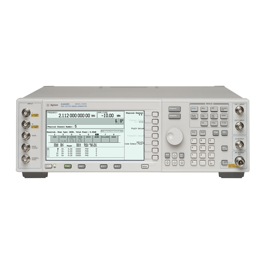
Page 30: Front Panel Overview
E4428C Analog Signal Generator Overview Front Panel Overview Front Panel Overview Figure 1-1 shows the signal generator front panel. This interface enables you to define, monitor, and manage input and output characteristics. Figure 1-1 Front Panel Feature Overview 1. Display The LCD screen provides information on the current function. -
Page 31: Frequency Key
50 to 1, then each turn of the knob changes the active function by 0.2 dB (1/50th of 10 dB). By modifying either value or both, you change the amount for each turn of the knob. For more information on softkeys, refer to the E4428C/38C ESG Signal Generators Key and Data Field Reference. 7. Save Key This hardkey accesses a menu of softkeys enabling you to save data to the signal generator’s instrument state... -
Page 32: Ext 1 Input Connector
E4428C Analog Signal Generator Overview Front Panel Overview 9. EXT 1 INPUT Connector This BNC input connector accepts an input signal for use with AM, FM, ΦM, and pulse modulation. The damage levels are 5 V and 10 V AM, FM, ΦM ±1 V... -
Page 33: Rf Output Connector
Changing the Incr Set hardkey’s value also affects how much each turn of the knob changes an active function’s value according to the knob’s current ratio setting. For more information on softkeys, refer to the E4428C/38C ESG Signal Generators Key and Data Field Reference. -
Page 34: Arrow Keys
E4428C Analog Signal Generator Overview Front Panel Overview 19. Arrow Keys The up and down arrow hardkeys are used to increase or decrease a numeric value, step through displayed lists, or select items in a row of a displayed list. Individual digits or characters may be highlighted using the left and right arrow hardkeys. -
Page 35: Power Switch
E4428C Analog Signal Generator Overview Front Panel Overview 28. Power Switch This switch activates full power to the signal generator when set to the on position, and deactivates all signal generator functions when in standby mode. In standby mode, the signal generator remains connected to the line power, and power is supplied to some internal circuits. -
Page 36: Front Panel Display
E4428C Analog Signal Generator Overview Front Panel Display Front Panel Display Figure 1-2 shows the front panel display. The LCD screen displays data fields, annotations, key press results, softkey labels, error messages, and annunciators that represent various active functions. Figure 1-2 Front Panel Display 1. -
Page 37: Annunciators
E4428C Analog Signal Generator Overview Front Panel Display 2. Annunciators The display annunciators show the status of some of the signal generator functions, and indicate error conditions. An annunciator position may be used by more than one function. This does not create a problem, because only one function that shares an annunciator position can be active at a given time. - Page 38 E4428C Analog Signal Generator Overview Front Panel Display This annunciator indicates if the RF carrier is modulated (MOD ON while there is an MOD ON/OFF active modulation format), or if the modulation is off (MOD OFF). Either condition of this annunciator is always visible in the display.
-
Page 39: Amplitude Area
The labels in this area define the function of the softkeys located immediately to the right of the label. The softkey label will change depending upon the function selected. For detailed softkey descriptions, refer to the E4428C/38C ESG Signal Generators Key and Data Field Reference. 5. Error Message Area Abbreviated error messages are reported in this space. -
Page 40: Rear Panel Overview
E4428C Analog Signal Generator Overview Rear Panel Overview Rear Panel Overview The signal generator rear panel (Figure 1-3) provides input, output, and remote interface connections. Figure 1-4 shows a portion of the rear panel for signal generators with Option 1EM, which moves front panel connectors to the rear panel. -
Page 41: Ac Power Receptacle
E4428C Analog Signal Generator Overview Rear Panel Overview 1. AC Power Receptacle The power cord receptacle accepts a three-pronged cable that is shipped with the signal generator. The line voltage is connected here. 2. GPIB Connector The GPIB connector allows communications with compatible devices such as external controllers. It is functionally equivalent to the LAN and RS 232 connectors. -
Page 42: Lan Connector
The LAN connector enables the signal generator to be remotely programmed by a LAN-connected computer. The distance between a computer and the signal generator is limited to 100 meters (10Base-T) on a single cable. For more information about the LAN, refer to the E4428C/38C ESG Signal Generators Programming Guide. -
Page 43: E4438C Vector Signal Generator Overview
E4438C Vector Signal Generator Overview This chapter provides a general overview of the Agilent E4438C ESG Vector Signal Generator and includes the following major sections: • “Standard Vector Signal Generator Features” on page 20 • “Options” on page 21 • “Firmware Upgrades”... -
Page 44: Standard Vector Signal Generator Features
E4438C Vector Signal Generator Overview Standard Vector Signal Generator Features Standard Vector Signal Generator Features • CW output from 250 kHz to 1, 2, 3, 4 or 6 GHz; the high-end frequency is dependent on the frequency option purchased with your signal generator •... -
Page 45: Options
E4438C Vector Signal Generator Overview Options Options ESG signal generators have hardware, firmware, software, and documentation options. The data sheet shipped with your signal generator provides an overview of available options. For more information, visit the Agilent ESG web page at http://www.agilent.com/find/esg, selected the desired ESG model, and then Options click the tab. -
Page 46: Firmware Upgrades
PC. 6. In the “Documents and Downloads” table, click the link in the “Upgrade Assistant Software” column for the E4428C/38C ESG to download the PSG/ESG Upgrade Assistant. 7. In the File Download window, select 8. In the Welcome window, click and follow the on-screen instructions. -
Page 47: Calibration
When the User Attention message appears, you must first cycle the instrument’s power, then click OK. When the upgrade completes, the Upgrade Assistant displays a summary. 15. Click and close the Upgrade Assistant. Calibration Agilent Technologies recommends calibrating the E4438C ESG Signal Generator every two years. Chapter 2... -
Page 48: Modes Of Operation
E4438C Vector Signal Generator Overview Modes of Operation Modes of Operation The ESG signal generator provides four modes of operation: • continuous wave (CW) • swept signal • analog modulation • digital modulation Continuous Wave In this mode, the signal generator produces a CW signal. The signal generator is set to a single frequency and power level. - Page 49 E4438C Vector Signal Generator Overview Modes of Operation • Custom Real Time I/Q Baseband mode produces a single carrier, but it can be modulated with real-time data that allows real-time control over all of the parameters that affect the signal. The single-carrier signal that is produced can be modified by applying various data patterns, filters, symbol rates, modulation types, and burst shapes.
-
Page 50: Front Panel Overview
E4438C Vector Signal Generator Overview Front Panel Overview Front Panel Overview Figure 2-1 shows the signal generator front panel. This interface enables you to define, monitor, and manage input and output characteristics. Figure 2-1 Front Panel Feature Overview 1. Display The LCD screen provides information on the current function. -
Page 51: Amplitude Key
50 to 1, then each turn of the knob changes the active function by 0.2 dB (1/50th of 10 dB). By modifying either value or both, you change the amount for each turn of the knob. For more information on softkeys, refer to the E4428C/38C ESG Signal Generators Key and Data Field Reference. 6. Menu Keys These hardkeys access softkey menus enabling configuration of list and step sweeps, utility functions, the LF output, and various analog and digital modulation types. -
Page 52: Ext 1 Input Connector
E4438C Vector Signal Generator Overview Front Panel Overview 9. EXT 1 INPUT Connector This BNC input connector accepts an input signal for use with AM, FM, ΦM, and pulse modulation, or as the linear control for a burst envelope. The damage levels are 5 V and 10 V AM, FM, ΦM ±1 V... -
Page 53: Lf Output Connector
Options 501, 502, 503, and 504 the reverse power protection circuit will trip, however, at nominally 1 W. CAUTION E4428C and E4438C signal generators with Option 506 are not equipped with reverse power protection circuits. On signal generators with Option 1EM, this output relocated to a rear-panel female Type-N connector. -
Page 54: Incr Set Key
Changing the Incr Set hardkey’s value also affects how much each turn of the knob changes an active function’s value according to the knob’s current ratio setting. For more information on softkeys, refer to the E4428C/38C ESG Signal Generators Key and Data Field Reference. -
Page 55: Standby Led
E4438C Vector Signal Generator Overview Front Panel Overview 26. Standby LED This yellow LED indicates when the signal generator power switch is set to the standby condition. 27. Line Power LED This green LED indicates when the signal generator power switch is set to the on position. 28. -
Page 56: Data Connector (Option 001/601 Or 002/602)
E4438C Vector Signal Generator Overview Front Panel Overview 31. DATA Connector (Option 001/601 or 002/602) The female BNC input connector accepts a CMOS externally supplied CMOS compatible signal data input used with digital modulation applications. The expected input is a CMOS signal where a CMOS high is equivalent to a data 1 and a CMOS low is equivalent to a data 0. -
Page 57: Front Panel Display
E4438C Vector Signal Generator Overview Front Panel Display Front Panel Display Figure 2-2 shows the front panel display. The LCD screen displays data fields, annotations, key press results, softkey labels, error messages, and annunciators that represent various active functions. Figure 2-2 Front Panel Display 1. -
Page 58: Annunciators
E4438C Vector Signal Generator Overview Front Panel Display 2. Annunciators The display annunciators show the status of some of the signal generator functions, and indicate error conditions. An annunciator position may be used by more than one function. This does not create a problem, because only one function that shares an annunciator position can be active at a given time. - Page 59 E4438C Vector Signal Generator Overview Front Panel Display This annunciator indicates if the RF carrier is modulated (MOD ON while there is an MOD ON/OFF active modulation format), or if the modulation is off (MOD OFF). Either condition of this annunciator is always visible in the display. The MOD ON annunciator may be showing even when there are no active modulation formats.
-
Page 60: Digital Modulation Annunciators
The labels in this area define the function of the softkeys located immediately to the right of the label. The softkey label will change depending upon the function selected. For detailed softkey descriptions, refer to the E4428C/38C ESG Signal Generators Key and Data Field Reference. 6. Error Message Area Abbreviated error messages are reported in this space. -
Page 61: Rear Panel Overview
E4438C Vector Signal Generator Overview Rear Panel Overview Rear Panel Overview The signal generator rear panel (Figure 2-3) provides input, output, and remote interface connections. Figure 2-4 shows a portion of the rear panel for signal generators with Option 1EM, which moves front panel connectors to the rear panel. -
Page 62: In Connector (Option 300)
E4438C Vector Signal Generator Overview Rear Panel Overview 1. 321.4 IN Connector (Option 300) Use this female SMB connector to input a downconverted 321.4 MHz GSM/EDGE signal for base transceiver station (BTS) loopback measurements. (Option 300 also requires Options UN7, 001/601or 002/602, and 402). -
Page 63: I Out Connector (Option 001/601 Or 002/602)
E4438C Vector Signal Generator Overview Rear Panel Overview If you configure your signal generator with Option 1EM, this output is relocated and changed from a BNC to an SMB connector. 6. I OUT Connector (Option 001/601 or 002/602) This female BNC connector outputs the analog, in-phase component of I/Q modulation from the internal baseband generator. -
Page 64: Q-Bar Out Connector (Option 001/601 Or 002/602)
E4438C Vector Signal Generator Overview Rear Panel Overview 9. Q-bar OUT Connector (Option 001/601 or 002/602) This female BNC connector is used in conjunction with the Q OUT connector to provide a balanced baseband stimulus. Balanced signals are signals present in two separate conductors that are symmetrical relative to ground, and are opposite in polarity (180 degrees out of phase). -
Page 65: Patt Trig In Connector (Option 001/601 Or 002/602)
E4438C Vector Signal Generator Overview Rear Panel Overview output on the EVENT 1 connector occurs whenever Marker 1 is turned on in the waveform.The output on the EVENT 2 connector occurs whenever Marker 2 is turned on in the waveform. (Markers are automatically turned on whenever you set them in a waveform segment. - Page 66 E4438C Vector Signal Generator Overview Rear Panel Overview Connector Pin Description (Continued) EVENT 3 Pin-19 of the Aux I/O connector is used with an internal baseband generator. In arbitrary waveform mode, this pin outputs a timing signal generated by Marker 3. The marker 3 output level is +3.3 V CMOS regardless of marker polarity settings.The reverse damage levels for this connector pin are >...
-
Page 67: Digital Bus
E4438C Vector Signal Generator Overview Rear Panel Overview Figure 2-5 AUX I/O Pin Configuration View looking into rear panel connector 14. DIGITAL BUS This is a proprietary bus used for Agilent Baseband Studio products, which require Option 601 or 602. This connector is not operational for general purpose customer use. -
Page 68: Gpib Connector
The LAN connector enables the signal generator to be remotely programmed by a LAN-connected computer. The distance between a computer and the signal generator is limited to 100 meters (10Base-T) on a single cable. For more information about the LAN, refer to the E4428C/38C ESG Signal Generators Programming Guide. -
Page 69: Trig Out Connector
E4438C Vector Signal Generator Overview Rear Panel Overview 19. TRIG OUT Connector This female BNC connector outputs a TTL signal that is asserted high at the start of a dwell sequence, or at the start of waiting for the point trigger in manual sweep mode. It is asserted low when the dwell is over, when the point trigger is received, or once per sweep during an LF sweep. -
Page 70: Mhz Out Connector
E4438C Vector Signal Generator Overview Rear Panel Overview 24. 10 MHz OUT Connector This female BNC connector provides a nominal signal level of +3.9 dBm ±2 dB, and an output impedance of 50Ω. The accuracy is determined by the timebase used. 25. -
Page 71: Basic Operation
Basic Operation The following list shows the topics covered in this chapter: • “Using Table Editors” on page 48 • “Configuring the RF Output” on page 50 • “Generating the Modulation Format” on page 58 • “Modulating the Carrier Signal” on page 60 •... -
Page 72: Using Table Editors
Basic Operation Using Table Editors Using Table Editors The signal generator table editors enable you to simplify configuration tasks, such as creating a list sweep. This section familiarizes you with basic table editor functionality using the List Mode Values table editor as an example. -
Page 73: Modifying Table Items In The Data Fields
Basic Operation Using Table Editors Table Editor Softkeys The following table editor softkeys are used to load, navigate, modify, and store table item values. Press More (1 of 2) Load/Store to access and its associated softkeys. Edit Item displays the selected item in the active function area of the display where the item’s value can be modified. -
Page 74: Configuring The Rf Output
Basic Operation Configuring the RF Output Configuring the RF Output This section will show you how to create continuous wave and swept RF outputs. Configuring a Continuous Wave RF Output Using these procedures, you will learn how to set the following parameters: •... - Page 75 Basic Operation Configuring the RF Output 6. Press the up arrow key. Incr Set Each press of the up arrow key increases the frequency by the increment value last set with the hardkey. The increment value is displayed in the active entry area. 7.
- Page 76 Basic Operation Configuring the RF Output Freq Offset 7. Press > > This enters a 1 MHz offset. The FREQUENCY area displays 2.000 000 00 MHz, which is the frequency output by the hardware (701 MHz) minus the reference frequency (700 MHz) plus the offset (1 MHz).
-
Page 77: Configuring A Swept Rf Output
Basic Operation Configuring the RF Output RF On/Off. 4. Press The display annunciator has changed from RF OFF to RF ON. The power at the RF OUTPUT connector is −20 dBm. Incr Set 5. Press > > This changes the amplitude increment value to 10 dB. 6. - Page 78 Basic Operation Configuring the RF Output values are swept from the start frequency/amplitude to the stop frequency/amplitude. When set to Down, values are swept from the stop frequency/amplitude to the start frequency/amplitude. Configuring and Activating a Single Step Sweep In this procedure, you will create a step sweep with nine, equally spaced points and the following parameters: •...
- Page 79 Basic Operation Configuring the RF Output Return Sweep Freq & Ampl 11. Press > > This sets the step sweep to sweep both frequency and amplitude data. Selecting this softkey returns you to the previous menu and turns on the sweep function. RF On/Off 12.
- Page 80 Basic Operation Configuring the RF Output Sweep Type List Step 2. Press This toggles the sweep type from step to list. Configure List Sweep 3. Press This opens another menu displaying softkeys that you will use to create the sweep points. The display shows the current list data.
- Page 81 Basic Operation Configuring the RF Output Insert Item 9. Highlight the frequency item for point 8, then press Insert Item Pressing shifts frequency values down one row, beginning at point 8. Note that the original frequency values for both points 8 and 9 shift down one row, creating an entry for point 10 that contains only a frequency value (the power and dwell time items do not shift down).
-
Page 82: Generating The Modulation Format
Basic Operation Generating the Modulation Format Generating the Modulation Format The modulation format can be turned on prior to or after setting your signal parameters. Perform the following steps to turn the modulation format on: 1. Access the first menu within the modulation format. This menu will show a softkey that has the format’s name associated with off and on. - Page 83 Basic Operation Generating the Modulation Format Figure 3-3 Modulation Format On Active Modulation Format Annunciator First AM Menu Modulation format is On Chapter 3...
-
Page 84: Modulating The Carrier Signal
Basic Operation Modulating the Carrier Signal Modulating the Carrier Signal Mod On/Off The carrier signal is modulated when the key is set to on and a modulation format is active. When the key is set to on, the MOD ON annunciator shows in the display. The MOD OFF annunciator appears when the key is set to off. -
Page 85: Creating And Applying User Flatness Correction
Basic Operation Creating and Applying User Flatness Correction Creating and Applying User Flatness Correction User flatness correction allows the digital adjustment of RF output amplitude for up to 1601 frequency points in any frequency or sweep mode. Using an Agilent E4416A/17A or E4418B/19B power meter (controlled by the signal generator through GPIB) to calibrate the measurement system, a table of power level corrections is created for frequencies where power level variations or losses occur. - Page 86 Basic Operation Creating and Applying User Flatness Correction Configure the Power Meter 1. Select SCPI as the remote language for the power meter. 2. Zero and calibrate the power sensor to the power meter. 3. Enter the appropriate power sensor calibration factors into the power meter as appropriate. 4.
- Page 87 Basic Operation Creating and Applying User Flatness Correction Figure 3-5 User Flatness Correction Equipment Setup Configure the Signal Generator Preset 1. Press 2. Configure the signal generator to interface with the power meter. Amplitude More (1 of 2) User Flatness More (1 of 2) Power Meter E4416A...
- Page 88 Basic Operation Creating and Applying User Flatness Correction Configure Step Array 4. Press This opens a menu for entering the user flatness step array data. Freq Start 5. Press > > Freq Stop 6. Press > > # of Points Enter 7.
- Page 89 Basic Operation Creating and Applying User Flatness Correction Performing the User Flatness Correction Manually If you are not using an Agilent E4416A/17A/18B/19B power meter, or if your power meter does not have a GPIB interface, complete the steps in this section and then continue with the user flatness correction tutorial. More (1 of 2) User Flatness Configure Cal Array...
- Page 90 Basic Operation Creating and Applying User Flatness Correction Applying a User Flatness Correction Array Return Return Flatness Off On Press > > This applies the user flatness correction array to the RF output. The UF indicator is activated in the AMPLITUDE section of the signal generator’s display and the frequency correction data contained in the correction array is applied to the RF output amplitude.
- Page 91 Basic Operation Creating and Applying User Flatness Correction GPIB Listener Mode 2. Press This presets the signal generator and returns it to GPIB listener mode. The signal generator can now receive remote commands executed by a remote controller connected to the GPIB interface. 3.
-
Page 92: Using The Memory Catalog
For more information on the memory catalog and performing these tasks remotely, see the E4428C/38C ESG SCPI Command Reference and the E4428C/38C ESG Vector Signal Generator Programming Guide. -
Page 93: Storing Files
Basic Operation Using the Memory Catalog Storing Files To store a file to the memory catalog, first create a file. For this example, use the default list sweep table. Preset 1. Press Sweep/List Configure L1ist Sweep More (1 of 2) Load/Store 2. -
Page 94: Using The Instrument State Registers
“Storing Files” on page 69. Refer to the E4428C/38C ESG Signal Generator Programming Guide and the E4428C/38C ESG Signal Generator Key and Data Field Reference for more information on the save and recall function. The following procedure demonstrates saving settings to the instrument state memory. -
Page 95: Saving An Instrument State
Basic Operation Using the Instrument State Registers Saving an Instrument State 1. Preset the signal generator, then turn on amplitude modulation (the AM annunciator will turn on): Frequency a. Press > > Amplitude b. Press > > AM Off On c. -
Page 96: Recalling An Instrument State
Basic Operation Using the Instrument State Registers Recalling an Instrument State Using this procedure, you will learn how to recall instrument settings saved to an instrument state register. Refer to the “Recalling an Instrument State for a Waveform File” on page 73 for recalling a waveform file and associated signal generator settings. -
Page 97: Recalling An Instrument State For A Waveform File
Basic Operation Using the Instrument State Registers Load Segment From NVWFM Memory Return 6. Press > 7. Scroll to the waveform selected in step 3. Select Waveform ARB Off On 8. Press > to on. This causes the signal generator to play the waveform. Saving the Instrument State Instrument states can be saved to any one of the 10 sequences and 100 registers in instrument state memory. -
Page 98: Deleting Registers And Sequences
Basic Operation Using the Instrument State Registers Deleting Registers and Sequences These procedures describe how to delete registers and sequences saved to an instrument state register. Deleting a Specific Register within a Sequence Preset 1. Press Recall Save 2. Press the hardkey. -
Page 99: Using Security Functions
All security functions described in this section also have an equivalent SCPI command for remote operation. (Refer to the “System Subsystem (:SYSTem)” chapter of the E4428C/38C ESG Signal Generators SCPI Command Reference for more information.) Understanding Memory Types The ESG comprises several memory types, each used for storing a specific type of data. - Page 100 Basic Operation Using Security Functions Table 3-1 Base Instrument Memory (Continued) Memory Type Purpose/Contents Data Input Method Location in Instrument and Remarks and Size Main factory firmware upgrades CPU board (same chip as firmware memory, Memory calibration/configuration data and user-saved data but managed separately) (Flash) user file system, which...
- Page 101 Basic Operation Using Security Functions Table 3-1 Base Instrument Memory (Continued) Memory Type Purpose/Contents Data Input Method Location in Instrument and Remarks and Size Calibration factory factory or service motherboard Backup calibration/configuration data only Memory backup (Flash) no user data 512 KB Boards factory calibration and...
-
Page 102: Removing Sensitive Data From Memory
Basic Operation Using Security Functions Table 3-2 Baseband Generator Memory (Options 001/601 and 002/602) (Continued) Memory Type Purpose/Contents Data Input Method Remarks and Size Coprocessor operating memory of During normal This memory is used during normal baseband Memory baseband coprocessor operation, some user generator operation. - Page 103 Basic Operation Using Security Functions Erase All CAUTION Do not use this function with signal generator firmware revisions C.04.84, C.04.86, or C.04.95. If you have one of these revisions installed, please upgrade immediately to revision C.04.96 or later. This function removes all user files, user flatness calibrations, user I/Q calibrations, and resets all table editors with original factory values, ensuring that user data and configurations are not accessible or viewable.
- Page 104 Basic Operation Using Security Functions Erase and Sanitize All CAUTION Do not use this function with signal generator firmware revisions C.04.84, C.04.86, or C.04.95. If you have one of these revisions installed, please upgrade immediately to revision C.04.96 or later. This function performs the same actions as Erase and Overwrite All and then adds more overwriting actions.
- Page 105 Basic Operation Using Security Functions User IQ Cal File (Vector Models Only) When a user-defined IQ calibration has been performed, the cal file data is removed by setting the cal file to default, as follows: I/Q Calibration Revert to Default Cal Settings On the front panel, press: >...
-
Page 106: Using The Secure Display
Keep the hard disk and send the instrument to a repair facility. When the instrument is returned, reinstall the hard disk. For procedures on removing and replacing the processor board and hard disk, refer to the E4428C/38C ESG Signal Generators Service Guide. - Page 107 Basic Operation Using Security Functions Figure 3-6 ESG Screen with Secure Display Activated Chapter 3...
-
Page 108: Enabling Options (E4438C Only)
Basic Operation Enabling Options (E4438C Only) Enabling Options (E4438C Only) You can retrofit a signal generator after purchase to add new capabilities. Some new optional features are implemented in hardware that you must install. Some options are implemented in software but require the presence of optional hardware in the instrument. -
Page 109: Waveform Licenses
Basic Operation Enabling Options (E4438C Only) 4. Enable the software option: a. Highlight the desired option. Modify License Key b. Press , and enter the 12-character license key (from the license key certificate). c. Verify that you want to reconfigure the signal generator with the new option: Proceed With Reconfiguration Confirm Change >... -
Page 110: Using The Web Server
Basic Operation Using the Web Server Using the Web Server You can communicate with the signal generator using the Web Server. This service uses TCP/IP (Transmission Control Protocol/Internet Protocol) to communicate with the signal generator over the internet. The Web Server uses a client/server model where the client is the web browser on your PC or workstation and the server is the signal generator. - Page 111 Use the softkey to select a Manual or DHCP (dynamic host communication protocol) LAN configuration. Refer to E4428C/38C ESG Signal Generator Key and Data Field Reference for more information. 6. Press the enter key on the computer’s keyboard. The web browser will display the signal generator’s...
- Page 112 Basic Operation Using the Web Server 7. Click the Signal Generator Web Control menu button on the left of the page. A new web page will be displayed as shown below in Figure 3-8. Figure 3-8 Web Page Front Panel This web page remotely accesses all signal generator functions and operations.
-
Page 113: Basic Digital Operation
Basic Digital Operation This chapter provides digital operation information. These features are available only in E4438C ESG Vector Signal Generators with Option 001/601or 002/602. The following list shows the topics covered in this chapter: • “Custom Modulation” on page 90 •... -
Page 114: Custom Modulation
Basic Digital Operation Custom Modulation Custom Modulation For creating custom modulation, the signal generator offers two modes of operation: the Arb Waveform Generator mode and the Real-Time I/Q Baseband mode. The Arb Waveform Generator mode has built-in modulation formats such as NADC or GSM and pre-defined modulation types such as BPSK and 16QAM that can be used to create a signal. -
Page 115: Custom Real Time I/Q Baseband
Basic Digital Operation Custom Modulation Custom Real Time I/Q Baseband The real-time mode simulates single-channel communication using user-defined modulation types along with custom FIR filters, and symbol rates. Data can be downloaded from an external source into PRAM memory or supplied as real time data using an external input. The Real-Time I/Q Baseband mode can also generate pre-defined data formats such as PN9 or FIX4. -
Page 116: Arbitrary (Arb) Waveform File Headers
(WFM1) and is named AUTOGEN_WAVEFORM. The default file header has no signal generator settings saved to it and the default marker file consists of all zeros. Refer to the E4428C/38C ESG Signal Generators Programming Guide for more information on marker files. - Page 117 Basic Digital Operation Arbitrary (ARB) Waveform File Headers When you turn the modulation format off, the AUTOGEN_WAVEFORM file remains in volatile waveform memory (WFM1) and can be selected again for playing only by the dual ARB player. If you turn on another Arb modulation format or change ESG parameters and settings, the AUTOGEN_WAVEFORM file will be overwritten by a new AUTOGEN_WAVEFORM, file header, and marker file.
-
Page 118: Modifying Header Information
Basic Digital Operation Arbitrary (ARB) Waveform File Headers Figure 4-1 First-Level Softkey Menu First-Level Softkey Menu Not all ARB formats have a Second Page Modifying Header Information This procedure builds on the previous procedure, explaining the different fields of a file header, and showing how to access, modify, and save changes to the file header information. - Page 119 Basic Digital Operation Arbitrary (ARB) Waveform File Headers Figure 4-2 CDMA2000 Default Header Display Lets you Enter/Edit the Description Field Clears the Saved Header Settings Column to Default Settings Saves the Current Inst. Settings Column to the Saved Header Settings Column Current Signal Generator Settings...
- Page 120 Basic Digital Operation Arbitrary (ARB) Waveform File Headers Runtime Scaling: The Runtime scaling value. Runtime scaling is applied in real-time while the waveform is playing. This setting can be changed only for files playing in the dual ARB player. Marker 1...4 Polarity: The marker polarity, positive or negative (described on page 144).
- Page 121 Basic Digital Operation Arbitrary (ARB) Waveform File Headers Figure 4-3 ARB Setup Softkey Menu and Marker Utilities * Opt 403 Dual ARB Player softkey Dual ARB Player Softkeys (They do not Appear in other Arb Formats) ARB Sample Clock 4. Set the ARB sample clock to 5 MHz: Press >...
- Page 122 Basic Digital Operation Arbitrary (ARB) Waveform File Headers Return Return Header Utilities 9. Return to the Header Utilities menu: Press > > Notice that the Current Inst. Settings column now reflects the changes made in steps 4 through 8 to the current signal generator setup, but that the saved header values have not changed (as shown in Figure 4-4 below).
- Page 123 Basic Digital Operation Arbitrary (ARB) Waveform File Headers Figure 4-5 Saved File Header Changes Page 1 Page 2 While a modulation format is active (on), the AUTOGEN_WAVEFORM waveform file plays and you can modify the header information. Once you turn the modulation format off, the header information is available only through the dual ARB player.
-
Page 124: Dual Arb Player Waveform Sequence File Headers
Basic Digital Operation Arbitrary (ARB) Waveform File Headers Dual ARB Player Waveform Sequence File Headers When you create a waveform sequence (described on page 108), the ESG automatically creates a default file header, which takes priority over the headers for the waveform segments that compose the waveform sequence. - Page 125 Basic Digital Operation Arbitrary (ARB) Waveform File Headers Select Waveform 3. Press the softkey. ARB Off On 4. Press to On. ARB Setup Header Utilities 5. Press > 6. Edit the file header. a. If you have a default file header, go to “Modifying Header Information”...
- Page 126 Basic Digital Operation Arbitrary (ARB) Waveform File Headers Figure 4-6 Viewing a File Header Header Editing Softkeys Grayed-Out file header and Current Signal Generator Settings Page 1 Page 2 Viewing a Different File Header You can view file headers for other waveform files, even while the dual ARB player has a waveform playing.
- Page 127 Basic Digital Operation Arbitrary (ARB) Waveform File Headers Figure 4-7 Waveform File List for Viewing a Different Header Current Waveform File Type Table Catalog Type 2. Press the softkey. Now you have a choice of three waveform file types that can be displayed in the table accessed in step one.
-
Page 128: Playing A Waveform File Containing A Header
Basic Digital Operation Arbitrary (ARB) Waveform File Headers WFM1 This choice will display all of the waveform segments that currently reside in volatile memory. NVWFM 3. Press the softkey. After pressing the softkey, you are returned to the waveform file listing table that now displays the waveform files from non-volatile memory. - Page 129 Basic Digital Operation Arbitrary (ARB) Waveform File Headers Figure 4-10 File Header Settings Applied Waveform is not Selected Preset Settings Applied Can change when a Waveform is Selected Summary Display Waveform Selected Saved Header Settings Applied Header Setting Applied Header Setting same as Preset Summary Display If you change any of the signal generator settings listed in the file header after the waveform file is selected,...
-
Page 130: Using The Dual Arb Waveform Player
ARB waveform player. For information on downloading waveforms, refer to the E4428C/38C ESG Signal Generator Programming Guide. The dual ARB player is used to rename and store waveform files and to load waveform files from the signal generator’s memory. -
Page 131: Creating Waveform Segments
There are two ways to provide waveform segments for use by the waveform sequencer. You can either download a waveform via the remote interface, or generate a waveform using one of the Arb modulation formats. For information on downloading waveforms via the remote interface, see the E4428C/38C ESG Signal Generator Programming Guide. -
Page 132: Creating A Waveform Sequence
Basic Digital Operation Using the Dual ARB Waveform Player 3. Generate the second waveform: Mode CDMA Arb IS-95A a. Press > > Setup Select 9 Ch Fwd b. Press > CDMA Off On c. Press until On is highlighted. CDMA Off On d. -
Page 133: Playing A Waveform Sequence
Basic Digital Operation Using the Dual ARB Waveform Player Mode Dual ARB Waveform Sequences Build New Waveform Sequence Insert Waveform a. Press > > > > Insert Selected Waveform b. Highlight the FWDCH_64 waveform segment and press Insert Selected Waveform c. -
Page 134: Editing A Waveform Sequence
Basic Digital Operation Using the Dual ARB Waveform Player 3. Configure the RF Output: a. Set the RF carrier frequency. b. Set the RF output amplitude. c. Turn on the RF output. The waveform sequence is now available at the signal generator’s RF OUTPUT connector. Editing a Waveform Sequence This procedure shows how to edit waveform segments within a waveform sequence, and then save the edited sequence with the segment changes. -
Page 135: Adding Real-Time Noise To A Dual Arb Waveform (Option 403)
Refer to the E4428C/38C ESG SCPI Command Reference for remote operation commands and the E4428C/38C ESG Signal Generator Key and Data Field Reference for key descriptions. -
Page 136: Storing And Loading Waveform Segments
Basic Digital Operation Using the Dual ARB Waveform Player for the purpose of C/N, is applied across a carrier bandwidth of 40 MHz. The default noise bandwidth factor is 1, which provides a flat noise signal bandwidth of a least 0.8 times the 50 MHz sample rate. Storing and Loading Waveform Segments Waveform segments can reside in volatile memory (WFM1), or they can be stored in non-volatile memory (NVWFM), or both. -
Page 137: Using Waveform 5-Pack Licensing (Options 221-229)
Basic Digital Operation Using the Dual ARB Waveform Player Enter c. Press d. Highlight the waveform segment that was renamed. Store Segment to NVWFM Memory 5. Press 6. Repeat steps three through five for all segments that you want to store. In addition to the above method for saving segments to NVWFM, the signal generator allows you to store all Store All to NVWFM Memory files, residing in WFM1, into NVWFM. - Page 138 Basic Digital Operation Using the Dual ARB Waveform Player Waveform 5-Pack licensing enables you to create and generate signals which can be saved for unlimited use in a signal generator (i.e. Waveform 5-Pack Option 22x is a perpetual fixed waveform license). Use the Signal Studio software to build and download waveforms to the signal generator’s volatile memory to be played.
- Page 139 Basic Digital Operation Using the Dual ARB Waveform Player 2. Redeem the N7699A-D01 that came with your copy of Option 22x. For more information on redeeming the N7699A-D01, refer to the E4438C-22x Entitlement Certificate. 3. Cycle the power on the signal generator. NOTE Anytime a new Option 22x is installed on the signal generator, you must cycle power on the 5-Pack License...
- Page 140 Basic Digital Operation Using the Dual ARB Waveform Player Figure 4-12 Add Waveform to 5-Pack Softkey Warning Message If the waveform selected for licensing has been verified as the waveform you want to be licensed, press Confirm Adding Waveform To 5-Pack. Caution! This step cannot be undone.
- Page 141 Basic Digital Operation Using the Dual ARB Waveform Player NOTE It is important to make a backup copy of any 5-Pack waveforms and store them on a computer or other media. Do not store the backup copy on the signal generator. If all of the copies of the waveforms are deleted or lost, then there is no way to recover the waveform or reassign the license.
- Page 142 Basic Digital Operation Using the Dual ARB Waveform Player Finding All Waveforms Associated with 5-Pack Licenses The following procedure displays a catalog of all of the Waveform 5-Pack files in the WFM1 memory, and the non-volatile storage (NVWFM): 1. On the signal generator: >...
- Page 143 Basic Digital Operation Using the Dual ARB Waveform Player Waveform 5-Pack Warning Messages Figure 4-13 This standard warning is displayed every time a waveform is selected to be licensed. This notification indicates that one of the available “license slot[s]” is about to be used from Option 22x.
-
Page 144: Understanding The I/Q Modulator Filter
Basic Digital Operation Understanding the I/Q Modulator Filter Understanding the I/Q Modulator Filter I/Q Mod Filter Manual Auto The I/Q modulator filter ( softkey) lets you select either post-reconstruction low pass filtering that has a narrower bandwidth than that of the reconstruction filter, or no post-reconstruction filtering. -
Page 145: Applying An I/Q Modulator Filter
Basic Digital Operation Understanding the I/Q Modulator Filter Applying An I/Q Modulator Filter Real-Time Signals 1. Configure the signal. 2. Set the I/Q modulator filter: More (1 of 2) I/Q Mod Filter Manual Auto a. Press > > I/Q Mod Filter This key is active only when using a real-time signal. -
Page 146: Local Settings For Arb Waveform Formats And The Dual Arb Player
Basic Digital Operation Local Settings for ARB Waveform Formats and the Dual ARB Player Local Settings for ARB Waveform Formats and the Dual ARB Player To provide you with the greatest convenience in optimizing and replicating waveforms for playback in the dual ARB player, settings that were previously (pre-C.03.10 firmware release) found in only the dual ARB player have now been incorporated into each of the ARB modulation formats. - Page 147 Basic Digital Operation Local Settings for ARB Waveform Formats and the Dual ARB Player SCPI command mnemonics. When an ARB format or the dual ARB player is active, the three softkeys in the I/Q and mux menus are grayed-out indicating that they do not apply to the ARB format or the dual ARB player.
-
Page 148: Waveform Runtime Scaling
Basic Digital Operation Local Settings for ARB Waveform Formats and the Dual ARB Player SCPI Command Changes New SCPI commands have been developed and included in the C.03.10 and later versions of the firmware. These new commands allow you to set the three parameters discussed earlier for each of the ARB modulation formats and the dual ARB player. -
Page 149: Waveform Markers
Basic Digital Operation Local Settings for ARB Waveform Formats and the Dual ARB Player would not be used in any of the other ARB modulation formats or the dual ARB player. If you were to turn off the CDMA2000 ARB format and then turn it back on, the factory setting would be applied until you once again change the ARB sample clock value. - Page 150 Basic Digital Operation Local Settings for ARB Waveform Formats and the Dual ARB Player of using the ALC hold feature may affect the waveform’s output amplitude. Amplitude The alternate amplitude marker function triggers the Alternate Amplitude feature located in the hardkey menu.
- Page 151 Basic Digital Operation Local Settings for ARB Waveform Formats and the Dual ARB Player Figure 4-15 ARB Marker Location and Softkey Menus First-Level Softkey Menu Not all ARB formats will have a Second Page * Opt. 403 softkey Chapter 4...
- Page 152 Basic Digital Operation Local Settings for ARB Waveform Formats and the Dual ARB Player Bluetooth Marker Behavior Bluetooth markers one and two have predetermined settings that are implemented when a payload data type is selected and the waveform is generated. A waveform is regenerated when a new payload data type is selected while the modulation format is on.
-
Page 153: Using Waveform Markers
Basic Digital Operation Using Waveform Markers Using Waveform Markers The signal generator provides four waveform markers to mark specific points on a waveform segment. When the signal generator encounters an enabled marker, an auxiliary output signal is routed to the rear panel event connector (described in the “Rear Panel Overview”... -
Page 154: Waveform Marker Concepts
Downloading a waveform file (as described in the E4428C/38C ESG Signal Generators Programming Guide) that does not have a marker file associated with it causes the signal generator to automatically create a marker file but does not place any marker points. - Page 155 Basic Digital Operation Using Waveform Markers segment could have different marker and routing settings. ALC Hold Marker Function While you can set a marker function (described as on the softkey label) either before or after Marker Routing you set marker points (page 137), setting a marker function before setting marker points may cause power spikes or loss of power at the RF output.
- Page 156 Basic Digital Operation Using Waveform Markers Example of Correct Use Waveform: 1022 points Marker range: 95-97 Marker polarity: Positive This example shows a marker set to sample the waveform’s area of highest amplitude. Note that the marker is set well before the waveform’s area of lowest amplitude.
- Page 157 Basic Digital Operation Using Waveform Markers Example of Incorrect Use Waveform: 1022 points Marker range: 110-1022 Marker polarity: Negative This figure shows that a negative polarity marker goes low during the marker on points; the marker signal goes high during the off Marker Marker On Marker On...
-
Page 158: Accessing Marker Utilities
Basic Digital Operation Using Waveform Markers Accessing Marker Utilities Use the following procedure to display the marker parameters. This procedure uses the dual ARB player, but you can access the marker utilities through the softkey in all ARB formats. ARB Setup 1. -
Page 159: Viewing Waveform Segment Markers
Basic Digital Operation Using Waveform Markers Viewing Waveform Segment Markers Markers are applied to waveform segments. Use the following steps to view the markers set for a segment (this example uses the factory-supplied segment, SINE_TEST_WFM). Set Markers 1. In the Marker Utilities menu (page 134), press 2. -
Page 160: Clearing Marker Points From A Waveform Segment
Basic Digital Operation Using Waveform Markers Clearing Marker Points from a Waveform Segment When you set marker points they do not replace points that already exist, but are set in addition to existing points. Because markers are cumulative, before you set points, view the segment (page 135) and remove any unwanted points. -
Page 161: Setting Marker Points In A Waveform Segment
Basic Digital Operation Using Waveform Markers Clearing a Single Marker Point Use the steps described in “Clearing a Range of Marker Points” on page 136, but set both the first and last marker point to the value of the point you want to clear. For example, if you want to clear a marker on point 5, set both the first and last value to 5. - Page 162 Basic Digital Operation Using Waveform Markers Placing a Marker on a Single Point On the First Point Marker Utilities Set Markers 1. In the menu (page 134), press 2. Highlight the desired waveform segment. In an ARB format, there is only one file (AUTOGEN_WAVEFORM) and it is already highlighted. 3.
-
Page 163: Controlling Markers In A Waveform Sequence (Dual Arb Only)
Basic Digital Operation Using Waveform Markers Apply To Waveform Return 8. Press > This causes the marker to occur on every other point (one sample point is skipped) within the marker point range, as shown below. Viewing markers is described on page 135 One application of the skipped point feature is the creation of a clock signal as the auxiliary output. - Page 164 Basic Digital Operation Using Waveform Markers 4. Name and store the waveform sequence “Storing Waveform Segments to Non-Volatile Memory” on page 112. The following figure shows a sequence built reusing the same factory-supplied waveform segment; a factory-supplied segment has a marker point on the first sample for all four markers. In this example, Marker 1 is enabled for the first segment, Marker 2 is enable for the second segment, and markers 3 and 4 are enabled for the third segment.
-
Page 165: Viewing A Marker Pulse
Basic Digital Operation Using Waveform Markers Return Name And Store Enter 6. Press > > The markers are enabled or disabled per your selections, and the changes have been saved to the selected sequence file. Sequence Marker Column This entry shows that only marker 3 is enabled for this segment. -
Page 166: Using The Rf Blanking Marker Function
Basic Digital Operation Using Waveform Markers 4. Connect the ESG’s rear-panel EVENT 1 output to the oscilloscope’s channel 2 input. When marker 1 is present, the ESG outputs a signal on the EVENT 1 connector as shown in the following example. RF Output Marker pulse on the Event 1 signal. - Page 167 Basic Digital Operation Using Waveform Markers Marker Routing Pulse/RF Blank Marker 1 Press > > Marker Polarity = Positive RF Signal When marker polarity is positive (the default setting), the RF output is blanked during the off maker points. ≈ 3.3V Marker Point 1...
-
Page 168: Setting Marker Polarity
Basic Digital Operation Using Waveform Markers Setting Marker Polarity Setting a negative marker polarity inverts the marker signal. Marker Utilities Marker Polarity 1. In the menu (page 134), press 2. Select the marker polarity as desired for each marker number. Default Marker Polarity = Positive Set each marker polarity independently. -
Page 169: Triggering Waveforms
Basic Digital Operation Triggering Waveforms Triggering Waveforms Triggering is available in both ARB and real-time formats. ARB triggering controls the playback of a waveform file; real-time custom triggering controls the transmission of a data pattern. The examples and discussions in this section use the dual ARB Player, but the functionality and methods of access (described page 147) are similar in all ARB and real-time formats. -
Page 170: Source
In real-time Custom, behavior depends on whether the signal uses framed or unframed data. Because the ESG provides only unframed data, to transmit a framed data signal you must create an external file that incorporates the framing and download it to the ESG (see the E4428C/38C ESG Signal Generators Programming Guide). -
Page 171: Accessing Trigger Utilities
Basic Digital Operation Triggering Waveforms Segment Advance • (dual ARB only) causes a segment in a sequence to require a trigger to play. The trigger source controls how play moves from segment to segment (example on page 150). A trigger received during the last segment loops play to the first segment in the sequence. -
Page 172: Setting The Polarity Of An External Trigger
Basic Digital Operation Triggering Waveforms Trigger Setup • To display the response selections available for a given trigger mode, press , then select the Retrigger Mode desired trigger mode. To see the selections for Single mode in an ARB format, select ;... - Page 173 Basic Digital Operation Triggering Waveforms This connection is applicable to all external triggering methods. The optional oscilloscope connection enables you to see the effect that the trigger signal has on the RF output. 2. Preset the signal generator. 3. Configure the carrier signal output: •...
-
Page 174: Using Segment Advance Triggering
Basic Digital Operation Triggering Waveforms Trigger Source Ext Source Patt Trig In 1 b. Press and note that for the softkey, the default selection is , which is the selection used in this example. 7. Generate the waveform: ARB Off On Press to On. -
Page 175: Using External Triggering
Basic Digital Operation Triggering Waveforms 2. Configure the RF output: • Set the desired frequency. • Set the desired amplitude. • Turn on the RF output. 3. Select a waveform sequence for playback: Mode Dual ARB Select Waveform a. Press >... - Page 176 Basic Digital Operation Triggering Waveforms Connecting the Equipment Connect the signal generator to the function generator, as shown in Figure 4-16. Figure 4-16 Configuring a Custom Multicarrier CDMA State Preset 1. Press Mode CDMA Arb IS-95A 2. Press > > Multicarrier Off On 3.
- Page 177 Basic Digital Operation Triggering Waveforms This generates a waveform with the custom multicarrier CDMA state configured in the previous section. The display changes to Multicarrier Setup: 4 CARRIERS. During waveform generation, the CDMA and I/Q annunciators activate and the new custom multicarrier CDMA state is stored in volatile ARB memory.
-
Page 178: Using Waveform Clipping
Basic Digital Operation Using Waveform Clipping Using Waveform Clipping Waveforms with high power peaks can cause intermodulation distortion, which generates spectral regrowth (a condition that interferes with signals in adjacent frequency bands). The clipping function enables you to reduce high power peaks by clipping the I and Q data to a selected percentage of its highest peak. The clipping feature is available only with the dual ARB mode. - Page 179 Basic Digital Operation Using Waveform Clipping The I and Q waveforms combine in the I/Q modulator to create an RF waveform. The magnitude of the RF envelope is determined by the equation , where the squaring of I and Q always results in a positive value.
-
Page 180: How Peaks Cause Spectral Regrowth
Basic Digital Operation Using Waveform Clipping How Peaks Cause Spectral Regrowth Because of the relative infrequency of high power peaks, a waveform will have a high peak-to-average power ratio (see Figure 4-19). Because a transmitter’s power amplifier gain is set to provide a specific average power, high peaks can cause the power amplifier to move toward saturation. -
Page 181: How Clipping Reduces Peak-To-Average Power
Basic Digital Operation Using Waveform Clipping How Clipping Reduces Peak-to-Average Power You can reduce peak-to-average power, and consequently spectral regrowth, by clipping the waveform. Clipping limits power peaks in waveforms by clipping the I and Q data to a selected percentage of its highest peak. - Page 182 Basic Digital Operation Using Waveform Clipping Figure 4-22 Rectangular Clipping Chapter 4...
- Page 183 Basic Digital Operation Using Waveform Clipping Figure 4-23 Reduction of Peak-to-Average Power Chapter 4...
-
Page 184: Configuring Circular Clipping
Basic Digital Operation Using Waveform Clipping Configuring Circular Clipping This procedure shows you how to configure circular clipping. The circular setting clips the composite I/Q data (I and Q data are clipped equally). For more information about circular clipping, refer to “How Clipping Reduces Peak-to-Average Power”... -
Page 185: Configuring Rectangular Clipping
Basic Digital Operation Using Waveform Clipping Configuring Rectangular Clipping This procedure shows you how to configure rectangular clipping. The rectangular setting clips the I and Q data independently. For more information about rectangular clipping, refer to “How Clipping Reduces Peak-to-Average Power” on page 157. -
Page 186: Using Waveform Scaling
Basic Digital Operation Using Waveform Scaling Using Waveform Scaling Waveform scaling is used to eliminate DAC over-range errors. The ESG provides two methods of waveform scaling: Runtime Scaling Available in the Dual ARB Player and the Multitone modulation format, this type of scaling enables you to make real-time scaling adjustments of a currently playing waveform. -
Page 187: How Scaling Eliminates Dac Over-Range Errors
Basic Digital Operation Using Waveform Scaling is unable to replicate the true form of the ripple (see Figure 4-25). As a result, the ESG reports a DAC over-range error. Figure 4-25 Waveform Overshoot How Scaling Eliminates DAC Over-Range Errors Scaling reduces or shrinks a baseband waveform’s amplitude while maintaining its basic shape and characteristics, such as peak-to-average power ratio. -
Page 188: Scaling A Currently Playing Waveform (Runtime Scaling)
Basic Digital Operation Using Waveform Scaling Figure 4-26 Waveform Scaling Although scaling maintains the basic shape of the waveform, too much scaling can compromise its integrity because the bit resolution can be so low that the waveform becomes corrupted with quantization noise. Maximum accuracy and optimum dynamic range are achieved by scaling the waveform just enough to remove the DAC over-range error. -
Page 189: Scaling A Waveform File In Volatile Memory
Basic Digital Operation Using Waveform Scaling ARB Setup More (1 of 2) Waveform Runtime Scaling 5. Press > > and adjust the front panel knob or use the number keys to enter a new value. The new scaling value is instantly applied to the playing waveform. Runtime scaling adjustments are not cumulative, as the values are always relative to original amplitude of the waveform file. -
Page 190: Using Customized Burst Shape Curves
Basic Digital Operation Using Customized Burst Shape Curves Using Customized Burst Shape Curves You can adjust the shape of the rise time curve and the fall time curve using the Rise Shape and Fall Shape editors. Each editor allows you to enter up to 256 values, equidistant in time, to define the shape of the curve. - Page 191 Basic Digital Operation Using Customized Burst Shape Curves User-Defined User-Defined Values Values Rise Fall Rise Fall Time Time Delay Delay Time Burst shape maximum rise and fall time values are affected by the following factors: • the symbol rate • the modulation type When the rise and fall delays equal 0, the burst shape is attempting to synchronize the maximum burst shape power to the beginning of the first valid symbol and the ending of the last valid symbol of the timeslot.
-
Page 192: Creating A User-Defined Burst Shape Curve
Basic Digital Operation Using Customized Burst Shape Curves The signal generator firmware computes optimum burst shape based on the settings you’ve chosen for modulation. You can further optimize burst shape by lining up the data portion with the modulation. For example, if you’re designing a new modulation scheme, do the following: •... - Page 193 Basic Digital Operation Using Customized Burst Shape Curves Accessing the Table Editors Preset 1. Press 2. Perform the following keypress sequence required for your format type. For Custom Format Mode Custom Real Time I/Q Base Band Burst Shape Press > >...
- Page 194 Basic Digital Operation Using Customized Burst Shape Curves Figure 4-27 Display the Burst Shape More (1 of 2) Display Burst Shape Press > This displays a graphical representation of the waveform’s rise and fall characteristics, as shown in Figure 4-28. Figure 4-28 To return the burst to the default conditions, press the following keys: Return...
-
Page 195: Storing A User-Defined Burst Shape Curve
Basic Digital Operation Using Customized Burst Shape Curves Storing a User-Defined Burst Shape Curve Define User Burst Shape More (1 of 2) Load/Store Store To File 1. Press > > > If there is already a file name from the Catalog of SHAPE Files occupying the active entry area, press the following keys: Editing Keys Clear Text... -
Page 196: Generating The Waveform
Basic Digital Operation Using Customized Burst Shape Curves Generating the Waveform Perform the following keypress sequence required for your format type. For Custom Format Return Custom Off On Press > For TMDA Formats Return Return More (2 of 2) desired format Off On Press >... -
Page 197: Using Finite Impulse Response (Fir) Filters
Basic Digital Operation Using Finite Impulse Response (FIR) Filters Using Finite Impulse Response (FIR) Filters Finite Impulse Response filters can be created and used with both dual arbitrary waveform generated waveforms and real-time baseband generated waveforms. For this example, the filter is defined within the CDMA2000 digital communications format, a dual arbitrary waveform generated state. - Page 198 Basic Digital Operation Using Finite Impulse Response (FIR) Filters Entering the Coefficient Values Return 1. Press the softkey to get to the first page of the table editor. Edit Item 2. Use the cursor to highlight the Value field for coefficient 0, then press 3.
- Page 199 Basic Digital Operation Using Finite Impulse Response (FIR) Filters Figure 4-30 Setting the Oversample Ratio The oversample ratio (OSR) is the number of filter coefficients per symbol. Acceptable values range from 1 through 32; the maximum combination of symbols and oversampling ratio allowed by the table editor is 1024.
- Page 200 Basic Digital Operation Using Finite Impulse Response (FIR) Filters Figure 4-31 Return. 2. Press Display Impulse Response 3. Press Refer to Figure 4-32. Figure 4-32 Return 4. Press to return to the menu keys. Chapter 4...
- Page 201 Basic Digital Operation Using Finite Impulse Response (FIR) Filters Storing the Filter to Memory Use the following steps to store the file. Load/Store Store To File 1. Press > . The catalog of FIR files appears along with the amount of memory available.
-
Page 202: Modifying A Fir Filter Using The Fir Table Editor
Basic Digital Operation Modifying a FIR Filter Using the FIR Table Editor Modifying a FIR Filter Using the FIR Table Editor FIR filters stored in signal generator memory can easily be modified using the FIR table editor. You can load the FIR table editor with coefficient values from user-defined FIR files stored in non-volatile memory or from one of the default FIR filters. -
Page 203: Modifying The Coefficients
Basic Digital Operation Modifying a FIR Filter Using the FIR Table Editor Modifying the Coefficients 1. Using the front-panel arrow keys, highlight coefficient 15. Enter 2. Press > Display Impulse Response 3. Press Figure 4-35 Refer to Figure 4-35 on page 179. -
Page 204: Differential Encoding
Basic Digital Operation Differential Encoding Differential Encoding Differential encoding is a digital-encoding technique whereby a binary value is denoted by a signal change rather than a particular signal state. Using differential encoding, binary data in any user-defined I/Q or FSK modulation can be encoded during the modulation process via symbol table offsets defined in the Differential State Map. -
Page 205: Differential Data Encoding
Basic Digital Operation Differential Encoding The following illustration shows a 4QAM modulation I/Q State Map. 2nd Symbol 1st Symbol Data = 00000001 Data = 00000000 Distinct values: -1, +1 Distinct values: +1, +1 3rd Symbol 4th Symbol Data = 00000010 Data = 00000011 Distinct values: -1, -1 Distinct values: +1, -1... -
Page 206: How Differential Encoding Works
Basic Digital Operation Differential Encoding For a bit-by-bit illustration of the encoding process, see the following illustration. 1 0 1 0 0 1 1 0 0 raw (unencoded) data change = no change = 1 1 1 differentially encoded data How Differential Encoding Works Differential encoding employs offsets in the symbol table to encode user-defined modulation schemes. - Page 207 Basic Digital Operation Differential Encoding These symbol table offsets will result in one of the transitions, as shown. Data Value 00000001 Data Value 00000000 with Symbol Table Offset -1 with Symbol Table Offset +1 transition 1 state backward transition 1 state forward Data Value 00000011 Data Value 00000010 with Symbol Table Offset +2...
-
Page 208: Using Differential Encoding
Basic Digital Operation Differential Encoding 1st Symbol 5th Symbol 3rd Symbol Data = 0011100001 4th Symbol 2nd Symbol Data Value Symbol Table Offset As you can see from the previous illustration, the 1st and 4th symbols, having the same data value (00), produce the same state transition (forward 1 state). - Page 209 Basic Digital Operation Differential Encoding Configuring User-Defined I/Q Modulation Preset 1. Press 2. Perform the following keypress sequence required for your format type. For Custom Format Mode Custom Real Time I/Q Base Band Modulation Type Define User I/Q Press > >...
- Page 210 Basic Digital Operation Differential Encoding Accessing the Differential State Map Table Editor Configure Differential Encoding Press This opens the Differential State Map table editor, as shown. At this point, you see the data for the 1st symbol (00000000) and the cursor prepared to accept an offset value.You are now prepared to create a custom differential encoding for the user-defined default 4QAM I/Q modulation.
- Page 211 Basic Digital Operation Differential Encoding Enter 3. Press > This encodes the third symbol by adding a symbol table offset of 2. The symbol rotates forward through the state map by 2 values when a data value of 10 is modulated. Enter 4.
-
Page 212: User-Defined I/Q Maps
Basic Digital Operation User-Defined I/Q Maps User-Defined I/Q Maps In modulation schemes defined by standards (such as TDMA and CDMA), symbols appear in default positions in the I/Q plane. Using the I/Q Values table editor, you can define your own symbol map by changing the position of one or more symbols. - Page 213 Basic Digital Operation User-Defined I/Q Maps Entering I and Q Values Enter the I and Q values listed in the following table. Symbol Data Bits I Value Q Value 0000 0.500000 1.000000 0001 −0.500000 1.000000 0010 0.500000 −1.000000 0011 −0.500000 −1.000000 Enter 1.
-
Page 214: Storing A User-Defined I/Q Map File
Basic Digital Operation User-Defined I/Q Maps Storing a User-Defined I/Q Map File In this example, you learn how to store a user-defined I/Q map. If you have not created a user-defined I/Q map, complete the steps in the previous sections, “Accessing and Clearing the I/Q Table Editor”... - Page 215 Basic Digital Operation User-Defined I/Q Maps Editing I and Q Values .235702 Enter 1. Press > .235702 Enter 2. Press > As you enter the numbers using the numeric keypad, they are displayed in the active entry area. If you make a mistake, use the backspace key and then retype.
-
Page 216: User-Defined Fsk Modulation
Basic Digital Operation User-Defined FSK Modulation User-Defined FSK Modulation Using the Frequency Values table editor, you can define, modify and store user-defined frequency shift keying modulation. The Frequency Values table editor is available for custom real-time I/Q baseband generator waveforms and real-time I/Q baseband generator TDMA waveforms. -
Page 217: Storing An Fsk Modulation
Basic Digital Operation User-Defined FSK Modulation As you modify the frequency deviation values, the cursor moves to the next data row. An unstored file of frequency deviation values is created for your custom 4-level FSK file. For instructions on storing the file, see the next section. - Page 218 Basic Digital Operation User-Defined FSK Modulation -600 3. Press > -1.8 4. Press > This sets the frequency deviation for data 0000, 0001, 0010, and 0011 to configure a user-defined FSK modulation. Each time you enter a value, the Data column increments to the next binary number, up to a total of 16 data values (from 0000 to 1111).
-
Page 219: Creating And Using Bit Files
A real-time digital modulation personality must be selected when desired real-time format appears in the key press path. NOTE For information on creating user-defined data files on a remote computer, see the E4428C/38C ESG Signal Generator Programming Guide. Creating a User File Accessing the Table Editor Preset 1. - Page 220 Basic Digital Operation Creating and Using Bit Files Offset Cursor Bit Data Hexadecimal Data File Name indicator (in Hex) Position indicator (in Hex) NOTE When you create new file, the default name appears as UNTITLED, or UNTITLED1, and so forth. This prevents overwriting previous files. Chapter 4...
-
Page 221: Renaming And Saving A User File
Basic Digital Operation Creating and Using Bit Files Entering Bit Values 1. Refer to the following figure. Enter These Bit Values Cursor Hexadecimal Data Position Indicator 2. Enter the 32 bit values shown. Bit data is entered into the table editor in 1-bit format. The current hexadecimal value of the binary data is shown in the Hex Data column, and the cursor position (in hexadecimal) is shown in the Position indicator. -
Page 222: Recalling A User File
Basic Digital Operation Creating and Using Bit Files Recalling a User File In this example, you learn how to recall a user-defined data file from the memory catalog. If you have not created and stored a user-defined data file, complete the steps in the previous sections, “Creating a User File”... -
Page 223: Applying Bit Errors To A User File
Basic Digital Operation Creating and Using Bit Files Inverting Bit Values 1011. 1. Press This inverts the bit values that are positioned 4C through 4F. Notice that hex data in this row has now changed to 76DB6DB6, as shown in the following figure. Hex Data changed Bits 4C through 4F inverted Applying Bit Errors to a User File... - Page 224 Basic Digital Operation Creating and Using Bit Files Chapter 4...
-
Page 225: Awgn Waveform Generator
AWGN Waveform Generator This chapter contains examples for using the additive white gaussian noise (AWGN) waveform generator. The AWGN waveform generator is available only for the E4438C Vector Signal Generator with Option 001/601or 002/602 and Option 403: • “Arb Waveform Generator AWGN” on page 202 •... -
Page 226: Configuring The Awgn Generator
AWGN Waveform Generator Configuring the AWGN Generator Configuring the AWGN Generator The AWGN (additive white Gaussian noise) generator is available for the Arb Waveform Generator mode and the Real Time I/Q Baseband mode. The AWGN generator can be configured with user-defined noise bandwidth, noise waveform length, and noise seed parameters. -
Page 227: Real Time I/Q Baseband Awgn
AWGN Waveform Generator Configuring the AWGN Generator Real Time I/Q Baseband AWGN Preset 1. Press Mode More (1 of 2) AWGN Real Time I/Q Baseband AWGN 2. Press > > > Bandwidth 3. Press > > Configuring the RF Output 1. - Page 228 AWGN Waveform Generator Configuring the AWGN Generator Chapter 5...
-
Page 229: Analog Modulation
Analog Modulation... -
Page 230: Analog Modulation Waveforms
Analog Modulation Analog Modulation Waveforms Analog Modulation Waveforms The signal generator can modulate the RF carrier with four types of analog modulation: amplitude, frequency, phase, and pulse. Available internal waveforms include: Sine sine wave with adjustable amplitude and frequency Dual-Sine dual-sine waves with individually adjustable frequencies and a percent-of- peak-amplitude setting for the second tone (available from function generator only) Swept-Sine... -
Page 231: Configuring Am
Analog Modulation Configuring AM Configuring AM Using these procedures, you will learn how to generate an amplitude-modulated RF carrier. Setting the Carrier Frequency Preset 1. Press Frequency 1340 2. Press > > Setting the RF Output Amplitude Amplitude Press > >... -
Page 232: Wideband Am (E4438C)
Analog Modulation Configuring AM Wideband AM (E4438C) Wideband AM offers bandwidth (up to 40 MHz) beyond that of standard internal AM (10 kHz) by utilizing an external modulating signal. The external modulating signal is connected to the front-panel I INPUT connector. -
Page 233: Configuring Fm
Analog Modulation Configuring FM Configuring FM Using this procedures, you will learn how to create a frequency-modulated RF carrier. Setting the RF Output Frequency Preset 1. Press Frequency 2. Press > > Setting the RF Output Amplitude Amplitude dBm. Press >... -
Page 234: Configuring Φm
Analog Modulation Configuring ΦM Configuring ΦM Using this procedures, you will learn how to create a phase-modulated RF carrier. Setting the RF Output Frequency Preset 1. Press Frequency 2. Press > > Setting the RF Output Amplitude Amplitude Press > >... -
Page 235: Configuring Pulse Modulation
Analog Modulation Configuring Pulse Modulation Configuring Pulse Modulation Using the following procedures, you will learn how to create a pulse-modulated RF carrier. Setting the RF Output Frequency Preset 1. Press Frequency 2. Press > > Setting the RF Output Amplitude Amplitude Press >... -
Page 236: Configuring The Lf Output
Analog Modulation Configuring the LF Output Configuring the LF Output The signal generator has a low frequency (LF) output. The LF output’s source can be switched between an internal modulation source or an internal function generator. Internal Monitor Using internal modulation ( ) as the LF output source, the LF output provides a replica of the signal from the internal source that is being used to modulate the RF output. -
Page 237: Configuring The Lf Output With An Internal Modulation Source
Analog Modulation Configuring the LF Output Configuring the LF Output with an Internal Modulation Source In this example, the internal FM modulation is the LF output source. NOTE Internal Monitor Internal modulation ( ) is the default LF output source. Configuring the Internal Modulation as the LF Output Source Preset 1. -
Page 238: Configuring The Lf Output With A Function Generator Source
Analog Modulation Configuring the LF Output Configuring the LF Output with a Function Generator Source In this example, the function generator is the LF output source. Configuring the Function Generator as the LF Output Source Preset 1. Press LF Out 2. -
Page 239: Digital Signal Interface Module
Digital Signal Interface Module This chapter provides information on the N5102A Baseband Studio Digital Signal Interface Module. These features are available only in E4438C ESG Vector Signal Generators with Options 003/004 and 601/602. Functions, features and operation of the N5102A are explained and demonstrated. •... -
Page 240: Clock Timing
Digital Signal Interface Module Clock Timing Clock Timing This section describes how clocking for the digital data is provided. Clock timing information and diagrams are supplied for the different port configurations (serial, parallel, or parallel interleaved data transmission) and phase and skew settings. All settings for the interface module are available on the signal generator user interface (UI). - Page 241 Digital Signal Interface Module Clock Timing Table 7-1 Warranted Parallel Output Level Clock Rates and Maximum Clock Rates Warranted Level Clock Rates Maximum Clock Rates (typical) Logic Type IQ Signal Type IQ Signal Type IF Signal Type IF Signal Type LVTTL and CMOS 100 MHz 100 MHz...
- Page 242 Digital Signal Interface Module Clock Timing Table 7-3 Output Serial Clock Rates Logic Type Minimum Rate Maximum Rate LVDS 1 x (word size) kHz 400 MHz LVTTL and CMOS 1 x (word size) kHz 150 MHz Table 7-4 Input Serial Clock Rates Logic Type Data Type Minimum Rate...
-
Page 243: Clock Source
Digital Signal Interface Module Clock Timing Table 7-5 Output Parallel and Parallel Interleaved Clock Rates Logic Type Signal Type Minimum Rate Maximum Rate LVDS 1 x (clocks/sample) kHz the smaller of: 100 x (clocks /sample) MHz 400 MHz 4 kHz 400 MHz Other 1 x (clocks/sample) kHz... -
Page 244: Common Frequency Reference
Digital Signal Interface Module Clock Timing The clock source is selected using the N5102A module UI on the signal generator, see Figure 7-2. Figure 7-2 Clock Source Selection External and Device selection: Set to match the clock rate of the applied clock signal Internal selection: Set the internal clock rate Internal clock source... - Page 245 Digital Signal Interface Module Clock Timing ESG Frequency Reference Connections When a frequency reference is connected to the signal generator, it is applied to one of two rear panel connectors: • 10 MHz IN • BASEBAND GEN REF IN The BASEBAND GEN REF IN connector will accept a frequency reference in the range of 1 to 100 MHz. If the external or device under test clock source cannot provide or accept a frequency reference, that clock signal can be applied to this connector and used as the frequency reference (as long as the frequencies are within the specified range).
- Page 246 Digital Signal Interface Module Clock Timing Figure 7-3 Frequency Reference Setup Diagrams for the N5102A Module Clock Signal Internally Generated Clock Device (DUT) Supplied Clock NOTE: Use only one of the two signal generator frequency reference inputs. Chapter 7...
-
Page 247: Clock Timing For Parallel Data
Digital Signal Interface Module Clock Timing Externally Supplied Clock NOTE: Use only one of the two signal generator frequency reference inputs. Clock Timing for Parallel Data Some components require multiple clocks during a single sample period. (A sample period consists of an I and Q sample). - Page 248 Digital Signal Interface Module Clock Timing Figure 7-4 Clock Sample Timing for Parallel Port Configuration 1 Clock Per Sample Clock and sample rates are the same 1 Sample Period 1 Clock Clock I sample 4 bits per word Q sample 4 bits per word Chapter 7...
- Page 249 Digital Signal Interface Module Clock Timing 2 Clocks Per Sample Sample rate decreases by a factor of two 1 Sample Period 2 Clocks Clock I sample 4 bits per word Q sample 4 bits per word 4 Clocks Per Sample Sample rate decreases by a factor of four 1 Sample Period 4 Clocks...
-
Page 250: Clock Timing For Parallel Interleaved Data
Digital Signal Interface Module Clock Timing Clock Timing for Parallel Interleaved Data The N5102A module provides the capability to interleave the digital I and Q samples. There are two choices for interleaving: • IQ, where the I sample is transmitted first •... - Page 251 Digital Signal Interface Module Clock Timing 2 Clocks Per Sample The I sample is transmitted for one clock period and the Q sample is transmitted during the second clock period; the sample rate decreases by a factor of two. 1 Sample Period 2 Clocks Clock I sample...
-
Page 252: Clock Timing For Serial Data
Digital Signal Interface Module Clock Timing Clock Timing for Serial Data Figure 7-6 shows the clock timing for a serial port configuration. Notice that the serial transmission includes frame pulses that mark the beginning of each sample where the clock delineates the beginning of each bit. For serial transmission, the clock and the bit rates are the same, but the sample rate varies depending on the Word Size number of bits per word that are entered using the... - Page 253 Digital Signal Interface Module Clock Timing Figure 7-7 Clock Phase and Skew Adjustments 90 degree phase adjustment Clock skew adjustment Phase and skew adjusted clock Phase adjusted clock Clock Data Chapter 7...
-
Page 254: Connecting The Clock Source And The Device Under Test
Digital Signal Interface Module Connecting the Clock Source and the Device Under Test Connecting the Clock Source and the Device Under Test As shown in Figure 7-3 on page 222, there are numerous ways to provide a common frequency reference to the system components (ESG, N5102A module, and the device under test). - Page 255 Digital Signal Interface Module Connecting the Clock Source and the Device Under Test 1. Refer to the five setup diagrams in Figure 7-3 on page 222 and connect the frequency reference cable according to the clock source. 2. If an external clock source is used, connect the external clock signal to the Ext Clock In connector on the interface module.
-
Page 256: Data Types
Digital Signal Interface Module Data Types Data Types The following block diagram indicates where in the ESG signal generation process the data is injected for input mode or tapped for output mode. Output Mode Pre-FIR Samples Samples Data Generator DACs Filtering Modulator Pre-FIR... - Page 257 Digital Signal Interface Module Data Types Table 7-7 Maximum Sample Rate for Selected Filter Filter Maximum Rate Gaussian Nyquist Root Nyquist Rectangle Edge 50 MHz UN3/4 GSM Gaussian IS-95 IS 95 w/EQ IS-95 Mod 25 MHz IS-95 Mod w/EQ APCO 25 C4FM 12.5 MHz Filter softkey accesses a menu that enables you set the desired filtering parameters.
-
Page 258: Operating The N5102A Module In Output Mode
Digital Signal Interface Module Operating the N5102A Module in Output Mode Operating the N5102A Module in Output Mode This section shows how to set the parameters for the N5102A module using the signal generator UI in the output direction. Each procedure contains a figure that shows the softkey menu structure for the interface module function being performed. -
Page 259: Choosing The Logic Type And Port Configuration
Digital Signal Interface Module Operating the N5102A Module in Output Mode Choosing the Logic Type and Port Configuration Figure 7-10 Logic and Port Configuration Softkey Menus 1. Refer to Figure 7-10. Press the softkey. Logic Type From this menu, choose a logic type. CAUTION Changing the logic type can increase or decrease the signal voltage level going to the device under test. -
Page 260: Selecting The Output Direction
Digital Signal Interface Module Operating the N5102A Module in Output Mode 4. Select the port configuration for the device. Selecting the Output Direction Press Data Setup > Direction Input Output to Output and press Return NOTE If Option 003 is the only option installed, the direction softkey will be unavailable and the mode will always be output. - Page 261 Digital Signal Interface Module Operating the N5102A Module in Output Mode Figure 7-12 Data Setup Softkey Menu with Parallel Port Configuration Inactive for ARB formats Inactive for word size = 16 bits Inactive for a serial port configuration Frame polarity is active for a serial port configuration Available only while in output mode...
-
Page 262: Configuring The Clock Signal
Digital Signal Interface Module Operating the N5102A Module in Output Mode 5. Select the numeric format required for the test. 6. Press the softkey. More (1 of 2) From this softkey menu, select the bit order, swap I and Q, select the polarity of the transmitted data, and access menus that provide data negation, scaling, gain, offset, and IQ rotation adjustments. - Page 263 Digital Signal Interface Module Operating the N5102A Module in Output Mode From this softkey menu, set all of the clock parameters that synchronize the clocks between the N5102A module and the ESG. You can also change the clock signal phase so the clock occurs during the valid portion of the data.
- Page 264 Digital Signal Interface Module Operating the N5102A Module in Output Mode This error is reported when the output FIFO is overflowing in the digital module. This error can be generated if an external clock or its reference is not set up properly, or if the internal VCO is unlocked.
- Page 265 Digital Signal Interface Module Operating the N5102A Module in Output Mode b. Press the softkey and enter the appropriate clock rate. Clock Rate Table 7-8 provides a quick view of the settings and connections associated with each clock source selection. Table 7-8 Clock Source Settings and Connectors Clock Source...
-
Page 266: Generating Digital Data
Digital Signal Interface Module Operating the N5102A Module in Output Mode 10. Enter the skew adjustment that best positions the clock with the valid portion of the data. 11. Press the softkey to Neg. Clock Polarity Neg Pos This shifts the clock signal 180 degrees, so that the data starts during the negative clock transition. This has the same affect as selecting the 180 degree phase adjustment. -
Page 267: Operating The N5102A Module In Input Mode
Digital Signal Interface Module Operating the N5102A Module in Input Mode Operating the N5102A Module in Input Mode This section shows how to set the parameters for the N5102A module using the signal generator UI in the input direction. Each procedure contains a figure that shows the softkey menu structure for the interface module function being performed. -
Page 268: Selecting The Input Direction
Digital Signal Interface Module Operating the N5102A Module in Input Mode Selecting the Input Direction If both Option 003 (output mode) and Option 004 (input mode) are installed, you must select the input direction. Press > to Input and press Data Setup Direction Input Output Return... -
Page 269: Configuring The Clock Signal
Digital Signal Interface Module Operating the N5102A Module in Input Mode 2. Select the logic type required for the device being tested. A caution message is displayed whenever a change is made to the logic types, and a softkey selection appears asking for confirmation. - Page 270 Digital Signal Interface Module Operating the N5102A Module in Input Mode This error is reported when the digital module clock setup is not synchronized with the rate the samples are entering the digital module. Verify that the input clock rate matches the specified clock rate under the clock setup menu.
- Page 271 Digital Signal Interface Module Operating the N5102A Module in Input Mode • clock skew adjustment • clock polarity selection 2. Press the softkey. Clock Source From this menu, select the clock signal source. With each selection, the clock routing display in the signal generator clock setup menu will change to reflect the current clock source.
- Page 272 Digital Signal Interface Module Operating the N5102A Module in Input Mode Table 7-9 Clock Source Settings and Connectors Clock Source Softkeys N5102A Module Connection Reference Freq Ref Ext Clock In Device Interface Clock Rate Frequency • • External • • Device •...
-
Page 273: Selecting The Data Parameters
Digital Signal Interface Module Operating the N5102A Module in Input Mode 9. Press the softkey to Neg. Clock Polarity Neg Pos This shifts the clock signal 180 degrees, so that the data starts during the negative clock transition. This has the same affect as selecting the 180 degree phase adjustment. 10. - Page 274 Digital Signal Interface Module Operating the N5102A Module in Input Mode Figure 7-20 Data Setup Softkey Menu with Parallel Port Configuration Inactive for a serial port configuration Frame polarity is active for a serial port configuration Only available when the N5102A digital module is Only available when turned on and using input mode...
-
Page 275: Digital Data
Digital Signal Interface Module Operating the N5102A Module in Input Mode 6. Press the softkey. More (1 of 2) From this softkey menu, select the bit order, swap I and Q, the polarity of the data, and access menus that provides data negation, scaling, and filtering parameters. - Page 276 Digital Signal Interface Module Operating the N5102A Module in Input Mode Chapter 7...
-
Page 277: Bluetooth Signals
Bluetooth Signals This feature is available only in E4438C ESG Vector Signal Generators with Option 001/601or 002/602. -
Page 278: Accessing The Bluetooth Setup Menu On The Esg
Bluetooth Signals Accessing the Bluetooth Setup Menu on the ESG Accessing the Bluetooth Setup Menu on the ESG Option 406 is required to perform the following procedure. This chapter will show you how to set up a sample Bluetooth packet with impairments that include additive white gaussian noise (AWGN) using the front panel keys of the ESG. -
Page 279: Setting Up Packet Parameters
Bluetooth Signals Setting Up Packet Parameters Setting Up Packet Parameters The steps in this procedure build upon the previous procedure. The signal generator uses a DH1 (Data-High rate) packet for the Bluetooth format. The DH1 packet is a single bundle of information transmitted within a piconet and covers a single timeslot. This packet consists of 3 entities: the access code, the header, and the payload. - Page 280 Bluetooth Signals Setting Up Packet Parameters AM_ADDR Enter 3. Press > > This sets the active member address and is used to distinguish between the active members participating on the piconet. NOTE The all-zero AM_ADDR is reserved for broadcast messages. Payload Data 8 Bit Pattern 10101010...
-
Page 281: Setting Up Impairments
Bluetooth Signals Setting up Impairments Setting up Impairments The steps in this procedure build upon the previous procedure. This procedure teaches you how to set up the parameters for the impairment function. Return Return Impairments 1. Press > > This accesses a menu which enables you to set up impairments. Freq Offset 2. - Page 282 Bluetooth Signals Setting up Impairments Return Impairments Off On 8. Press > to On. This returns you to the Impairments menu and turns the impairments function on. The following figure displays the impairment parameters. Chapter 8...
-
Page 283: Using Burst
Bluetooth Signals Using Burst Using Burst The steps in this procedure build upon the previous procedure. Return 1. Press to return to the top-level Bluetooth menu. Burst Off On 2. Notice that is set to On. When burst is on, the signal power ramps up prior to transmitting the packet and then ramps down at the end of the packet transmission. -
Page 284: Using Clock/Gate Delay
Bluetooth Signals Using Clock/Gate Delay Using Clock/Gate Delay The steps in this procedure build upon the previous procedure. This function is available only when the payload data is continuous PN9 and is intended to be used during bit error rate (BER) testing. Packet (DH1) Payload Data Continuous PN9... -
Page 285: Turning On A Bluetooth Signal
Bluetooth Signals Turning On a Bluetooth Signal Turning On a Bluetooth Signal This procedure builds upon the previous procedure. Bluetooth Off On Press to On. This turns the operating state of the Bluetooth signal generator on. The front panel I/Q and BLUETTH annunciators appear, and the signal builds. The following figure displays the Bluetooth signal parameters. - Page 286 Bluetooth Signals Turning On a Bluetooth Signal Chapter 8...
-
Page 287: Bert
BERT This feature is available only in E4438C ESG Vector Signal Generators with Option 001/601or 002/602. -
Page 288: Setting Up A Phs Bit Error Rate Test (Bert)
BERT Setting Up a PHS Bit Error Rate Test (BERT) Setting Up a PHS Bit Error Rate Test (BERT) This section shows how to make BERT measurements on a personal handyphone system (PHS) radio using the ESG Signal Generator with Option UN7. The following procedures explain how to set up the ESG for making BERT measurements: •... -
Page 289: Connecting The Test Equipment
BERT Setting Up a PHS Bit Error Rate Test (BERT) Connecting the Test Equipment Refer to Figure 9-1. 1. Connect the cables between your radio and the ESG as follows: Figure 9-1 Setup for a PHS Bit Error Rate Test Chapter 9... -
Page 290: Setting The Carrier Frequency And Power Level
BERT Setting Up a PHS Bit Error Rate Test (BERT) Setting the Carrier Frequency and Power Level Preset 1. Press the hardkey. Frequency 2. Press the hardkey. Using the numeric keypad, set the signal generator RF output carrier frequency to 1.89515 GHz. Amplitude 3. -
Page 291: Setting The Radio To A Receiver Mode
BERT Setting Up a PHS Bit Error Rate Test (BERT) Setting the Radio to a Receiver Mode Set the PHS radio to receive the signal of the specified carrier frequency and the timeslot 1, and output the data used for the bit error rate measurements. Selecting the BERT Data Pattern and Total Bits 1. -
Page 292: Starting Bert Measurements
BERT Setting Up a PHS Bit Error Rate Test (BERT) Starting BERT measurements Trigger Press the front panel hardkey to start the BERT measurement. You will see the measurement result values of the Total Bits, Error Bits, and BERT on the signal generator display. NOTE If you encounter problems making a BERT measurement, check the following: •... -
Page 293: Measuring Rf Loopback Bert With Option 300
BERT Measuring RF Loopback BERT with Option 300 Measuring RF Loopback BERT with Option 300 The following procedure uses the data looped back from the base transceiver station (BTS) to measure the bit error ratio introduced by the BTS receiver when it is receiving coded data from the test equipment. Timing synchronization must first be achieved between the BTS and the test equipment so that data can be transmitted and received at the expected times. - Page 294 BERT Measuring RF Loopback BERT with Option 300 Figure 9-2 BTS Loopback Test Equipment Setup NOTE This example uses an ARFCN of 124 for the BCH and synchronizes to the TCH midamble in timeslot 2 on ARFCN 124. You can substitute as appropriate for your BTS. All key presses assume factory defined defaults at preset.
-
Page 295: Configuring Gsm Mode On The Agilent Technologies E4406A Vsa Series Transmitter Tester
BERT Measuring RF Loopback BERT with Option 300 Configuring GSM Mode on the Agilent Technologies E4406A VSA Series Transmitter Tester The following steps will show you how to set up the vector signal analyzer (VSA) for synchronization. 1. To preset the VSA:... -
Page 296: Configuring Gsm Mode On The Esg Vector Signal Generator
BERT Measuring RF Loopback BERT with Option 300 Configuring GSM Mode on the ESG Vector Signal Generator The following steps will show you how to configure a timeslot with multiframe data, set up traffic channel 1, and set the frequency and amplitude in GSM mode on the signal generator. When configuring a timeslot in this procedure, keep the following points in mind: •... - Page 297 BERT Measuring RF Loopback BERT with Option 300 Timeslot # Enter 5. Press > > Timeslot Type Normal Press > Configure Normal Multiframe Channel TCH/FS PN15 Press > > > > NOTE If the default training sequence (TSCO) does not match the training sequence sent by the Return Return BTS, press...
- Page 298 BERT Measuring RF Loopback BERT with Option 300 Figure 9-4 Amplitude −95 10. Press > > Amplitude Baseband BERT The amplitude can also be set using an softkey, located in the softkey menu, that Aux Fctn BERT Baseband BERT is accessed by pressing the >...
-
Page 299: Synchronizing To The Bch Then The Tch
BCH signal now. The BCH is only required to contain the synchronization logical channel (SCH). 1. Follow the instructions under “Configuring GSM Mode on the Agilent Technologies E4406A VSA Series Transmitter Tester” “Configuring GSM Mode on the ESG Vector Signal Generator”... - Page 300 BERT Measuring RF Loopback BERT with Option 300 Figure 9-7 5. Turn off the BCH signal. and set up the base station to send the TCH signal. 6. Set up the base station and start sending the TCH signal now. The TCH is only required to contain a valid midamble.
-
Page 301: Synchronizing To The Tch
If the base station is transmitting a BCH signal, turn it off at this time. 1. Follow the instructions under “Configuring GSM Mode on the Agilent Technologies E4406A VSA Series Transmitter Tester” “Configuring GSM Mode on the ESG Vector Signal Generator”... -
Page 302: Making Loopback Bert Measurements
BERT Measuring RF Loopback BERT with Option 300 Return GSM BERT Off On to On. 6. Press > NOTE If the following error message is generated: 522 Demodulator Unleveled; Input amplitude underrange this indicates that the TCH signal is not being received. Synchronize to BCH/TCH/PDCH 7. - Page 303 BERT Measuring RF Loopback BERT with Option 300 Pass/Fail Limits Class II RBER 4. Press > > > Return Threshold # of Events to Stop Class II Bit Error Enter 5. Press > > > > Class II Bit Error Notice that the softkey is highlighted, 300 events is displayed beneath the softkey, and Stop Thrs: CII(300) appears in the status area of the display.
-
Page 304: Using Amplitude Sensitivity Search
BERT Measuring RF Loopback BERT with Option 300 Figure 9-11 NOTE To select an alternate trigger mode (for example, Immediate): Return Configure Triggers Press three times, then press > BERT Trigger Source Immediate > Using Amplitude Sensitivity Search This procedure shows you how to set a pass amplitude with high and low amplitude boundaries, and how to set both the target error percentage, and the frame count for an amplitude sensitivity search. - Page 305 BERT Measuring RF Loopback BERT with Option 300 Figure 9-12 Frame Count Enter 4. Press > > Target % 5. Press > > Pass Amplitude −95 6. Press > > High Amplitude −86 7. Press > > Low Amplitude −104 8.
- Page 306 BERT Measuring RF Loopback BERT with Option 300 Figure 9-13 Trigger 10. Press to start the measurement: After the search is complete, Pass or Fail is displayed on the lower left corner of the screen, when either of the following occurs: •...
- Page 307 BERT Measuring RF Loopback BERT with Option 300 Figure 9-14 Stop Sensitivity Search 11. Press to terminate a measurement: NOTE To select an alternate trigger mode (for example, Immediate): Return Configure Triggers BERT Trigger Source Immediate Press > > > NOTE For efficiency, the search routine uses shorter measurements initially with the final measurements being over the frame length selected.
-
Page 308: Using The External Frame Trigger Function With The Edge Format
BERT Using the External Frame Trigger Function with the EDGE Format Using the External Frame Trigger Function with the EDGE Format NOTE Frame Trigger Source BCH PDCH This function is available only when the is set to PDCH. The External Frame Trigger Function is used to adjust the burst timing at PDCH synchronization. This requires calculating a delay value and then adjusting the initial value. -
Page 309: Adjusting The Delay Value
BERT Using the External Frame Trigger Function with the EDGE Format Figure 9-16 8. Calculate the offset value X using the following equation: ) 3.693 ⁄ X symbols D 227.8 – Where, in the EDGE mode, 3.693 µs is equal to 1 symbol. Adjusting the Delay Value 1. - Page 310 BERT Using the External Frame Trigger Function with the EDGE Format Figure 9-17 Aux Fctn BERT BTS BERT EDGE Loopback 2. Press > > EDGE BERT Configure Triggers 3. Press to On > Frame Trigger Source BCH PDCH 4. Press to PDCH.
- Page 311 BERT Using the External Frame Trigger Function with the EDGE Format Configure Triggers Ext Frame Trigger Delay 8. Press > 9. Change the delay value by rotating the knob slowly to find the range of delay values that display a Ready status.
-
Page 312: Bit Error Rate Tester-Option Un7
BERT Bit Error Rate Tester–Option UN7 Bit Error Rate Tester–Option UN7 The bit error rate test (BERT) capability allows you to perform bit error rate (BER) analysis on digital communications equipment. This enables functional and parametric testing of receivers and components including sensitivity and selectivity. -
Page 313: Clock/Gate Delay Function
BERT Bit Error Rate Tester–Option UN7 The following figure shows an example of the clock gate signal. Figure 9-19 Clock Gate Off On • When the softkey is set to Off: The clock signal in both “A” and “B” parts is effective and no gate function is required. Therefore, the bit error rate is measured using the clock and data signal in both “A”... -
Page 314: Clock Delay Function
BERT Bit Error Rate Tester–Option UN7 Figure 9-20 Clock Delay Function In this example, the clock delay function is off. Figure 9-21 shows the input of the internal error detector of UN7 through AUX I/O and indicates that the data is delayed from the clock. Chapter 9... - Page 315 BERT Bit Error Rate Tester–Option UN7 Figure 9-21 CH1: BER TEST OUT (pin 20 of AUX I/O connector) CH2: BER MEAS END (pin 1 of AUX I/O connector) In this example, the clock delay function is on. The rising edge of the clock was delayed by 200 ns and was adjusted to the center of the data.
-
Page 316: Gate Delay Function In The Clock Mode
BERT Bit Error Rate Tester–Option UN7 Gate Delay Function in the Clock Mode To use this function, the clock must be set to continuous mode. In this example, the clock is used to delay the gate function. The clock of the internal error detector was gated by the gate signal which is delayed by two clocks. - Page 317 BERT Bit Error Rate Tester–Option UN7 Figure 9-24 In this example, the triggering sequence is where you have an incoming data clock and data bit sequences, the trigger is active, and the BERT measurement begins. Refer to Figure 9-25. Chapter 9...
- Page 318 BERT Bit Error Rate Tester–Option UN7 Figure 9-25 In this example, synchronization occurs after receiving a trigger. The reference data is generated by stored data bits. If the BERT measurement accepts data bits immediately after receiving a trigger, set the trigger delay to On and the trigger delay count to a value corresponding to the data format.
-
Page 319: Data Processing
BERT Bit Error Rate Tester–Option UN7 The reference data is generated by stored data bits. If the BERT measurement accepts data bits immediately after receiving a trigger, set the trigger delay to On and the trigger delay count to a value corresponding to the data format. -
Page 320: Repeat Measurements
BERT Bit Error Rate Tester–Option UN7 Special Pattern Ignore Function The special pattern ignore function is especially useful when performing BERT analysis on radios that generate consecutive 0’s or 1’s data for traffic channels when they fail to detect the Unique Word or lose Spcl Pattern synchronization. -
Page 321: Testing Signal Definitions
BERT Bit Error Rate Tester–Option UN7 Figure 9-29 Testing Signal Definitions The timing diagram Figure 9-30, “Testing Signal Definitions,” shows the relationships between a trigger event and the output signals at the BER MEAS END and BER TEST OUT connectors. If a BER MEAS END signal stays high following a trigger event, the BERT measurement is in progress and other trigger events are ignored. - Page 322 BERT Bit Error Rate Tester–Option UN7 • T1 is a firmware handling time measured from a Trigger event to the rising edge of a BER MEAS END signal. • T2 is a firmware handling time measured from the falling edge of a BER TEST OUT signal to the falling edge of the BER MEAS END signal.
-
Page 323: Rf Loopback Ber-Option 300
BERT RF Loopback BER–Option 300 RF Loopback BER–Option 300 Synchronization Synchronizing the test equipment to the base transceiver station (BTS) is a prerequisite to the BTS looping back the selected traffic channel (TCH). This can be achieved in two ways: BCH Sync or TCH Sync. BCH Sync The BTS is set to transmit to the test equipment a BCH on timeslot 0 of a selected absolute radio frequency channel number (ARFCN). -
Page 324: Erased Frame Detection
BERT RF Loopback BER–Option 300 Erased Frame Detection When an incorrect CRC in an uplink speech frame is detected by a BTS conforming to the GSM standards, the BTS substitutes an all-zero speech frame. In the loopback mode, the BTS transmitter then recodes this substituted zero speech frame before transmission back to the test equipment receiver (VSA/ESG). - Page 325 BERT RF Loopback BER–Option 300 Table 9-1 GSM Received Data (Continued) During BCH Synchronization TS1-7 No SCH, but otherwise, don’t care During TCH Synchronization 26-frame TCH Multiframe Structure Frame 25 idle Frame 12 don’t care Other frames TCH During Measurements Timeslot under test 26-frame full-rate voice TCH Multiframe Structure Content determined by transmitted signal (looped by BTS except...
-
Page 326: Verifying Bert Operation
BERT Verifying BERT Operation Verifying BERT Operation This procedure verifies the operation of the signal generator’s bit error rate test (BERT) function. This test can be performed as part of a daily validation routine or can be used whenever you want to check the validity of your BERT measurements. - Page 327 BERT Verifying BERT Operation Preset 2. Press the hardkey. This configures the signal generator to a pre-defined state. Mode 3. Press the hardkey. Real TDMA Data Format 4. Press > > to Pattern. Data PN Sequence PHS Off On 5. Press >...
- Page 328 BERT Verifying BERT Operation Bit Delay Off On BERT Trigger 13. Press to Off > to Trigger Key. Trigger 14. Press the hardkey. The following figure shows the signal generator’s front-panel display after completion of the these steps. BERT Verification BERT Trigger 1.
- Page 329 If the verification procedures produce the expected results, then the signal generator BERT measurement function is operating correctly. If the above procedure produces unexpected results, then contact the Agilent Service Center. For a list of Agilent Service Centers, refer to the E4428C/38C ESG Signal Generators Installation Guide.
- Page 330 BERT Verifying BERT Operation Chapter 9...
-
Page 331: Cdma Digital Modulation
CDMA Digital Modulation This feature is available only in E4438C ESG Vector Signal Generators with Option 001/601or 002/602. -
Page 332: Cdma2000 Forward Link Modulation For Component Test
CDMA Digital Modulation cdma2000 Forward Link Modulation for Component Test cdma2000 Forward Link Modulation for Component Test This section teaches you how to build forward link cdma2000 waveforms for testing component designs. The waveforms are generated by the signal generator’s internal dual arbitrary waveform generator. Activating a Predefined CDMA Forward Link State This procedure teaches you how to perform the following tasks: •... -
Page 333: Creating A User-Defined Cdma Forward Link State
CDMA Digital Modulation cdma2000 Forward Link Modulation for Component Test Creating a User-Defined CDMA Forward Link State This procedure teaches you how to perform the following tasks: • “Accessing the Table Editor with the Default Forward Link Setup” on page 309 •... - Page 334 CDMA Digital Modulation cdma2000 Forward Link Modulation for Component Test Edit Item 4800 3. Press > 4. Highlight the Walsh code value (8) in table row 3. Edit Item Enter. 5. Press > > 6. Highlight the Power value (−12.72) in table row 3. Edit Item −10 7.
- Page 335 CDMA Digital Modulation cdma2000 Forward Link Modulation for Component Test Inserting Additional cdma2000 Forward Link Traffic Channels Edit Channel Setup 1. Press Insert Row Traffic Channels Enter 2. Move cursor to the bottom row and press > > > > Done 3.
-
Page 336: Cdma2000 Reverse Link Modulation For Component Test
CDMA Digital Modulation cdma2000 Reverse Link Modulation for Component Test cdma2000 Reverse Link Modulation for Component Test This section teaches you how to build reverse link cdma2000 waveforms for testing component designs. The waveforms are generated by the signal generator’s internal dual arbitrary waveform generator. Activating a Predefined cdma2000 Reverse Link State This procedure teaches you how to perform the following tasks: •... -
Page 337: Creating A User-Defined Cdma2000 Reverse Link State
CDMA Digital Modulation cdma2000 Reverse Link Modulation for Component Test Creating a User-Defined cdma2000 Reverse Link State This procedure teaches you how to perform the following tasks: • “Accessing the Table Editor with the Default Reverse Link Setup” on page 313 •... - Page 338 CDMA Digital Modulation cdma2000 Reverse Link Modulation for Component Test 4. Highlight the Power value (–17.36) in table row 3. Edit Item −10 5. Press > > The display shows that the total power is now at 0.34 dB. You can rescale the total channel power to Adjust Code Domain Power Scale to 0 dB 0 dB by pressing...
- Page 339 CDMA Digital Modulation cdma2000 Reverse Link Modulation for Component Test The channel table editor now contains the an additional supplemental2 traffic channel. The display shows that the total power is now at 1.37 dB. You can rescale the total channel power to 0 dB by Adjust Code Domain Power Scale to 0 dB pressing...
-
Page 340: Storing A Component Test Waveform To Memory
CDMA Digital Modulation Storing a Component Test Waveform to Memory Storing a Component Test Waveform to Memory In this section, you will learn how to store the component test waveform. Mode Setup 1. Press hardkey to return to the top-level menu. 2. -
Page 341: Recalling A Component Test Waveform
CDMA Digital Modulation Recalling a Component Test Waveform Recalling a Component Test Waveform In this section, you will learn how to recall a component test waveform. Mode Setup 1. Press hardkey to return to the top-level menu. 2. Perform the following keypress sequence required for your format type. For CDMA2000 Waveform Format CDMA2000 Select Custom CDMA2000 State... -
Page 342: Creating A Custom Multicarrier Cdma2000 Waveform
CDMA Digital Modulation Creating a Custom Multicarrier cdma2000 Waveform Creating a Custom Multicarrier cdma2000 Waveform The signal generator provides a quick and easy way to create custom multicarrier cdma2000 waveforms: rather than building an entire 4-carrier setup from scratch, you can start with a 4-carrier cdma2000 template and modify the template’s default values as desired. -
Page 343: Modifying A Multicarrier Cdma2000 4-Carrier Template
CDMA Digital Modulation Creating a Custom Multicarrier cdma2000 Waveform Figure 10-7 Modifying a Multicarrier cdma2000 4-Carrier Template Use the tasks to modify the standard 4-carrier cdma2000 template that was loaded in the previous procedure. 1. Highlight the second channel carrier in table row 2. Edit Item SR3 Direct Pilot 2. -
Page 344: Activating A Custom Multicarrier Cdma2000 Setup
CDMA Digital Modulation Creating a Custom Multicarrier cdma2000 Waveform Figure 10-8 Activating a Custom Multicarrier cdma2000 Setup Using the custom 4-carrier cdma2000 setup from the previous procedure, perform the following task to activate the custom multicarrier cdma2000 signal. Return More (2 of 2) CDMA2000 Off On 1. - Page 345 CDMA Digital Modulation Creating a Custom Multicarrier cdma2000 Waveform After waveform generation, the new multicarrier cdma2000 waveform is stored in volatile memory. The CDMA2K and I/Q annunciators appear on the display and the RF ON annunciator replaces the RF OFF annunciator, as shown in the following figure.
-
Page 346: Cdma2000 Forward Link Modulation For Receiver Test
CDMA Digital Modulation cdma2000 Forward Link Modulation for Receiver Test cdma2000 Forward Link Modulation for Receiver Test This section teaches you how to build cdma2000 forward link signals for testing mobile receiver designs. The signals are generated by the internal real-time IQ baseband generator. The procedures in this section build on each other and are designed to be used sequentially. - Page 347 CDMA Digital Modulation cdma2000 Forward Link Modulation for Receiver Test Changing Channel States This task teaches you how to quickly configure the operating states of the forward link channels. Mode Setup 1. Press to return to the top-level real-time cdma2000 menu. Link Control Channel State Quick Presets All (Except FQPCH)
-
Page 348: Adjusting Code Domain Power
CDMA Digital Modulation cdma2000 Forward Link Modulation for Receiver Test Figure 10-10 Forward Fundamental Channel (F-FCH) Setup Note that the ESG allows you to set the relative channel power for each active channel. To display the normalized relative channel power after completing the setup, it is recommended that you perform the steps “Adjusting Code Domain Power”... -
Page 349: Managing Noise
CDMA Digital Modulation cdma2000 Forward Link Modulation for Receiver Test The power level displayed for each channel is now changed to show the normalized relative channel power. Scale to 0 dB Figure 10-11 shows the displayed power levels before and after the softkey is pressed. -
Page 350: Generating The Baseband Signal
CDMA Digital Modulation cdma2000 Forward Link Modulation for Receiver Test • “Setting EbNo” on page 326 Setting the Carrier to Noise Ratio Mode Setup 1. Press to return to the top-level real-time cdma2000 menu. Noise Setup 2. Press > > >... -
Page 351: Configuring The Rf Output
CDMA Digital Modulation cdma2000 Forward Link Modulation for Receiver Test Configuring the RF Output The steps in this procedure build upon the previous procedure. 1. Set the RF output frequency to 2.14 GHz. 2. Set the output amplitude to −30 dBm. RF On/Off 3. -
Page 352: Cdma2000 Reverse Link Modulation For Receiver Test
CDMA Digital Modulation cdma2000 Reverse Link Modulation for Receiver Test cdma2000 Reverse Link Modulation for Receiver Test This section teaches you how to build cdma2000 reverse link signals for testing base station receiver designs. The signals are generated by the internal real-time IQ baseband generator. The procedures in this section build on each other and are designed to be used sequentially. - Page 353 CDMA Digital Modulation cdma2000 Reverse Link Modulation for Receiver Test Link Control Operating Mode RadioConfig 1/2 Access 2. Press > > Notice that the display shows a single reverse access channel. This is an IS-2000 standard channel configuration. For learning purposes, we will change back to RadioConfig 3/4 Traffic, which is the default operating mode.
-
Page 354: Adjusting Code Domain Power
CDMA Digital Modulation cdma2000 Reverse Link Modulation for Receiver Test You have now modified the reverse fundamental channel parameters so that the radio configuration is 4, the data is a fixed 4-bit pattern of 1010, the relative channel power is −10 dB, and EbNo value is 12 dB. Figure 10-13 shows what the display should look like when this task is completed. -
Page 355: Managing Noise
CDMA Digital Modulation cdma2000 Reverse Link Modulation for Receiver Test Link Control Adjust Code Domain Power Scale to 0 dB 2. Press > > The power level displayed for each channel is now changed to show the normalized relative channel power. Scale to 0 dB Figure 10-14 shows the displayed power levels before and after the... -
Page 356: Generating The Baseband Signal
CDMA Digital Modulation cdma2000 Reverse Link Modulation for Receiver Test • “Setting the Carrier to Noise Ratio” on page 332 • “Setting EbNo” on page 332 Setting the Carrier to Noise Ratio Mode Setup 1. Press to return to the top-level real-time cdma2000 menu. Noise Setup 2. -
Page 357: Configuring The Rf Output
CDMA Digital Modulation cdma2000 Reverse Link Modulation for Receiver Test Configuring the RF Output The steps in this procedure build upon the previous procedure. 1. Set the RF output frequency to 2.14 GHz. 2. Set the output amplitude to −30 dBm. RF On/Off 3. -
Page 358: Applying A User-Defined Fir Filter To A Cdma2000 Waveform
CDMA Digital Modulation Applying a User-Defined FIR Filter to a cdma2000 Waveform Applying a User-Defined FIR Filter to a cdma2000 Waveform Custom FIR filters can be created using the FIR table editor feature or they can be created externally and downloaded into signal generator memory. -
Page 359: Figure
CDMA Digital Modulation Applying a User-Defined FIR Filter to a cdma2000 Waveform Figure 10-17 Select The filter you selected is NEWFIR2. You can see the name displayed below the softkey. In the Filter field, near the left of the display, User FIR is displayed to indicate that a user-defined FIR filter has been selected. -
Page 360: Is-95A Modulation
CDMA Digital Modulation IS-95A Modulation IS-95A Modulation This section teaches you how to build dual arbitrary waveform generated IS-95A CDMA modulation for testing component designs. Creating a Predefined CDMA State This section teaches you how to perform the following tasks: •... -
Page 361: Creating A User-Defined Cdma State
CDMA Digital Modulation IS-95A Modulation Creating a User-Defined CDMA State In this procedure, you learn how to customize a predefined CDMA setup, starting with a forward 32 channel CDMA setup and modifying the setup by adding one channel and changing some of the setup’s default values. - Page 362 CDMA Digital Modulation IS-95A Modulation Modifying the Code Domain Power Adjust Code Domain Power IS-97 Levels Press > You now have a custom, forward 33 channel CDMA signal at IS-97 power levels, with an inserted traffic channel carrying user-defined data at a Walsh code of 45 on table row 8, as shown in the following figure. Generating the Waveform Return Return...
-
Page 363: Applying Changes To An Active Cdma State
CDMA Digital Modulation IS-95A Modulation Applying Changes to an Active CDMA State CDMA Off On If the CDMA format is currently in use ( set to On) while changes are made in the CDMA Channel Setup table editor, you must apply the changes before the updated waveform will be generated. From the CDMA Channel Setup table editor, press the following keys to apply the changes and generate a new user-defined CDMA waveform based on the updated values: Return... -
Page 364: Press Edit Item Khz
CDMA Digital Modulation IS-95A Modulation Modifying Carrier Frequency Offset 1. Highlight the Freq Offset value (0.00 kHz) for the new pilot carrier in row 3. Edit Item -625 2. Press > > Modifying Carrier Power 1. Highlight the Power value (0.00 dB) for the new pilot carrier in row 3. Edit Item 2. -
Page 365: Applying Changes To An Active Multicarrier Cdma State
CDMA Digital Modulation IS-95A Modulation Configuring the RF Output 1. Set the RF output frequency to 890.01 MHz. 2. Set the output amplitude to −10 dBm. RF On/Off 3. Press The user-defined multicarrier CDMA signal is now available at the RF OUTPUT connector. Applying Changes to an Active Multicarrier CDMA State CDMA Off On If the CDMA format is currently in use (... - Page 366 CDMA Digital Modulation IS-95A Modulation Chapter 10...
-
Page 367: Gps Modulation
GPS Modulation Option 409 includes real time multiple-satellite and single-satellite global positioning system (GPS) signal Mode More generation capabilities. Press > > to access the GPS menus. • “Real Time MSGPS” on page 344 (multiple satellite GPS) • “Real Time GPS” on page 351 (single satellite GPS) This feature is available only in E4438C ESG Vector Signal Generators with Option 001/601 or 002/602. -
Page 368: Real Time Msgps
GPS Modulation Real Time MSGPS Real Time MSGPS In Real Time MSGPS mode, selectable scenario files define simulated multiple-satellite conditions. The E4438C generates a signal (C/A code only) simulating multiple satellite transmissions from the information in the selected scenario file. MSGPS signal generation capabilities include: •... -
Page 369: Signal Generation Block Diagram
GPS Modulation Real Time MSGPS Signal Generation Block Diagram Figure 11-1 shows how the signal is generated within the ESG for a four satellite MSGPS simulation. The ESG produces a simulated signal for each satellite and then sums them together to produce the MSGPS Number of Satellites signal. -
Page 370: Scenario Files
GPS Modulation Real Time MSGPS Scenario Files When you install option 409, a GPS directory is created in the ESG non-volatile memory and two MSGPS scenario files are loaded into the GPS directory. Additional scenario files are available for Option 409. Options (Go to http://www.agilent.com/find/e4438c and click the tab.) After downloading a... -
Page 371: Rf Power Level Considerations
GPS Modulation Real Time MSGPS RF Power Level Considerations When you set up your GPS test signal, pay special attention to the RF power level delivered to the GPS receiver. Because typical GPS sensitivities are between −155 dBm and −159 dBm, delivering a GPS signal to your device with a power level greater than −150 dBm or less than −160 dBm may produce invalid test results. - Page 372 GPS Modulation Real Time MSGPS Table 11-1 describes each field for the first of the three GPGSV messages in the example: $GPGSV,3,1,12,21,71,000,,27,68,000,34,08,62,000,33,29,52,000,,*71 Table 11-1 GPGSV Fields GPGSV Field Description $GPGSV, Number of GPGSV messages in this set Number of this GPGSV in the set (1 of 3) Total number of satellites in view 21,71,000,, Satellite 21, elevation 71, azimuth 0, CNO unknown...
-
Page 373: Generating A Real Time Msgps Signal
GPS Modulation Real Time MSGPS Generating a Real Time MSGPS Signal This procedure uses the internal reference clock with the factory preset settings (the C/A chip rate is 1.023 Mcps with a clock reference of 10.23 Mcps). Set the carrier frequency and amplitude Preset 1. -
Page 374: Configuring The External Reference Clock
GPS Modulation Real Time MSGPS Figure 11-2 Real Time MSGPS Scenario Configuring the External Reference Clock 1. Connect the external reference clock source to the DATA CLOCK INPUT connector. 2. Set the chip rate of the external clock to the desired value. Mode More (1 of 2) Real Time MSGPS... -
Page 375: Real Time Gps
GPS Modulation Real Time GPS Real Time GPS This real-time personality simulates GPS satellite transmissions for single channel receiver testing. Basic GPS signal building capabilities include: • P code generation at 10.23 Mcps with the standard GPS 10.23 Mcps reference •... -
Page 376: Real Time Gps Introduction
GPS Modulation Real Time GPS Real Time GPS Introduction Signal Generation Block Diagram Figure 11-3 shows how the GPS signal is generated within the ESG. Notice that the C/A code modulates the L-band signal using the I axis of the I/Q modulator, and the P code modulates the L-band signal using the Q Data axis. - Page 377 GPS Modulation Real Time GPS Data Modes and Subframe Structures You can select one of the three following data modes for use with the C/A or C/A+P ranging code: • Raw - The Raw data mode enables the continuous transmission of 300 bits of data per subframe without incorporating parity bits.
- Page 378 GPS Modulation Real Time GPS The TLM word is 30-bits long, with an 8-bit preamble, 16 reserve bits (bits 9 to 24, all set to zero), and 6 parity bits (bits 25 to 30). The HOW word is 30-bits long, with the first 17 bits used for an incrementing time-of-week (TOW), bits 23 and 24 used for parity computation, and bits 25 to 30 used for parity bits.
- Page 379 GPS Modulation Real Time GPS Rear Panel Signal Synchronization Figure 11-5 illustrates the timing relationships of the GPS signals available at the signal generator rear panel. The AUX I/O connector outputs the SYMBOL SYNC OUT, DATA CLOCK OUT, and DATA OUT signals (refer to, “13.
- Page 380 GPS Modulation Real Time GPS User Files You can create data files internally in the ESG or create them externally and download them to the ESG. In either case, the size of user data files is limited by the amount of available ESG memory. If you develop data files externally, you can define signal structures that are not available internally in the ESG.
-
Page 381: Setting Up The Real Time Gps Signal
GPS Modulation Real Time GPS Setting Up the Real Time GPS Signal Utility Power On/Preset Preset Normal User If the signal generator is in the factory-defined preset mode, ( > > Preset Normal) a basic GPS signal is automatically set up when you press the key. -
Page 382: Configuring The External Reference Clock
GPS Modulation Real Time GPS Figure 11-6 Real Time GPS Setup with Internal Clock Configuring the External Reference Clock Mode More(1 of 2) Real Time GPS 1. Access the real-time GPS personality ( > > > More (1 of 2) GPS Ref Clk Ext Int 2. - Page 383 GPS Modulation Real Time GPS Figure 11-7 Real Time GPS Setup with External Clock This procedure used an external source as the reference clock signal. The reference frequency was changed from the GPS standard of 10.23 Mcps to 11.03 kcps. This change in the reference signal frequency automatically changed the P and C/A code chip rates.
-
Page 384: Testing Receiver Sensitivity
GPS Modulation Real Time GPS Testing Receiver Sensitivity Refer to Figure 11-8. 1. Connect the cables between the receiver and the ESG as shown in Figure 11-8. Figure 11-8 Setup for a Receiver Sensitivity Test 2. Set the GPS data mode to TLM. 3. -
Page 385: Setting Up A Gps Bit Error Rate Test
GPS Modulation Real Time GPS Setting Up a GPS Bit Error Rate Test This section shows how to make GPS BER measurements using the ESG Signal Generator with Option UN7. The following procedures explain how to set up the ESG for making BER measurements: •... -
Page 386: Connecting The Test Equipment
GPS Modulation Real Time GPS Connecting the Test Equipment 1. Connect the cables between your receiver and the ESG as shown in Figure 11-9: Figure 11-9 Setup for a GPS Bit Error Rate Test Setting the Carrier Frequency and Power Level Preset 1. -
Page 387: Selecting The Data Format
GPS Modulation Real Time GPS Selecting the Data Format Mode More (1 or 2) Real Time GPS. 1. Press > > > 2. Ensure that Raw is the selected data mode. Data Mode Raw Enc TLM If Raw is not the current data mode, press to Raw. -
Page 388: Selecting The Bert Trigger
GPS Modulation Real Time GPS Selecting the BERT Trigger Return Configure Trigger 1. Press > BERT Trigger Trigger Key If the softkey does not show as the selected trigger, press BERT Trigger Trigger Key > Return BERT Off On 2. Press >... -
Page 389: Multitone Waveform Generator
Multitone Waveform Generator This feature is available only in E4438C ESG Vector Signal Generators with Option 001/601or 002/602. -
Page 390: Creating A Custom Multitone Waveform
Multitone Waveform Generator Creating a Custom Multitone Waveform Creating a Custom Multitone Waveform Using the Multitone Setup table editor, you can define, modify and store user-defined multitone waveforms. Multitone waveforms are generated by the dual arbitrary waveform generator. This section teaches you how to perform the following tasks: •... -
Page 391: Generating The Waveform
Multitone Waveform Generator Creating a Custom Multitone Waveform Generating the Waveform Multitone Off On Press until On is highlighted. This generates the multitone waveform with the parameters defined in the previous sections. During waveform generation, the M-TONE and I/Q annunciators activate and the multitone waveform is stored in volatile ARB memory. -
Page 392: Applying Changes To An Active Multitone Signal
Multitone Waveform Generator Applying Changes to an Active Multitone Signal Applying Changes to an Active Multitone Signal Multitone Off On If the multitone generator is currently in use ( set to On) while changes are made in the Multitone Setup table editor, you must apply the changes before the updated waveform will be generated. -
Page 393: Recalling A Multitone Waveform
Multitone Waveform Generator Applying Changes to an Active Multitone Signal Recalling a Multitone Waveform Using this procedure, you learn how to recall a multitone waveform from the signal generator’s memory catalog. If you have not created and stored a multitone waveform, complete the steps in the previous sections, “Creating a Custom Multitone Waveform”... - Page 394 Multitone Waveform Generator Applying Changes to an Active Multitone Signal Chapter 12...
-
Page 395: Custom Digital Modulation
Custom Digital Modulation This feature is available only in E4438C ESG Vector Signal Generators with Option 001/601or 002/602. -
Page 396: Using The Arbitrary Waveform Generator
Custom Digital Modulation Using the Arbitrary Waveform Generator Using the Arbitrary Waveform Generator This section teaches you how to build dual arbitrary (ARB) waveform generated custom TDMA digital modulation for testing component designs. Custom ARB digital modulation creates waveforms using modulation types, filtering, symbol rates, and other parameters defined by digital communications standards. -
Page 397: Creating A Custom Tdma Digital Modulation State
Custom Digital Modulation Using the Arbitrary Waveform Generator Creating a Custom TDMA Digital Modulation State In this procedure, you learn how to set up a single-carrier NADC digital modulation with customized modulation type, symbol rate, and filtering. This section teaches you how to perform the following tasks: •... -
Page 398: Storing A Custom Tdma Digital Modulation State
Custom Digital Modulation Using the Arbitrary Waveform Generator Configuring the RF Output 1. Set the RF output frequency to 835 MHz. 2. Set the output amplitude to 0 dBm. RF On/Off 3. Press The user-defined NADC signal is now available at the RF OUTPUT connector. Storing a Custom TDMA Digital Modulation State Using this procedure, you learn how to store a custom digital modulation state and a custom multicarrier digital modulation state to non-volatile memory. -
Page 399: Creating A Custom Multicarrier Tdma Digital Modulation State
Custom Digital Modulation Using the Arbitrary Waveform Generator Setup Select More (1 of 2) Custom Digital Mod State 2. Press > > 3. Highlight the desired file (for example, NADCQPSK). Select File 4. Press Digital Modulation Off On 5. Press until On is highlighted. - Page 400 Custom Digital Modulation Using the Arbitrary Waveform Generator Modifying Carrier Power 1. Highlight the Power value (0.00 dB) for the carrier in row 2. Edit Item 2. Press > > You now have a custom 2-carrier EDGE waveform with a carrier at a frequency offset of −625 kHz and a power level of −10.00 dBm, as shown in the following figure.
-
Page 401: Storing A Custom Multicarrier Tdma Digital Modulation State
Custom Digital Modulation Using the Arbitrary Waveform Generator Storing a Custom Multicarrier TDMA Digital Modulation State Using this procedure, you learn how to store a custom multicarrier TDMA digital modulation state to non-volatile memory. If you have not created a custom multicarrier digital modulation state, complete the steps in the previous section, “Creating a Custom Multicarrier TDMA Digital Modulation State”... -
Page 402: Using The Real Time I/Q Baseband Generator
Custom Digital Modulation Using the Real Time I/Q Baseband Generator Using the Real Time I/Q Baseband Generator The custom real-time format enables you to create unframed digital modulation with user-defined data, filtering, symbol rate, modulation type, burst shape, differential data encoding, and other format parameters. You can choose a predefined mode where filtering, symbol rate and modulation type are defined by the digital modulation standard, or a user-defined custom modulation. -
Page 403: Creating User-Defined Custom Modulation
Custom Digital Modulation Using the Real Time I/Q Baseband Generator Creating User-Defined Custom Modulation This section teaches you how to perform the following tasks: • “Selecting Data” on page 379 • “Configuring the Filter” on page 379 • “Selecting a Symbol Rate” on page 379 •... - Page 404 Custom Digital Modulation Using the Real Time I/Q Baseband Generator Configuring the Burst Rise and Fall Parameters Burst Shape Rise Time. 1. Press > 5.202 bits 2. Press > Rise Delay .667 bits 3. Press > > Fall Time bits 4.
-
Page 405: Real Time Tdma Formats
Real Time TDMA Formats In the following sections, this chapter provides the following information. These features are available only in E4438C ESG Vector Signal Generators with Option 001/601or 002/602. This chapter contains procedures on operating the real-time TDMA formats. The ESG generates the modulation for these formats using the ESG’s internal baseband generator. -
Page 406: Edge Framed Modulation
Real Time TDMA Formats EDGE Framed Modulation EDGE Framed Modulation This section describes how to build framed, real-time I/Q baseband generated EDGE and GMSK modulation for testing receiver designs. Each timeslot provides the flexibility of changing from the current modulation type to a GMSK modulation. The GMSK timeslot selection provides a normal GSM timelsot. The procedures in this section build on each other, so perform them sequentially. -
Page 407: Activating Framed Data Format
Real Time TDMA Formats EDGE Framed Modulation Activating Framed Data Format Preset 1. Press Mode Real Time TDMA EDGE Data Format Pattern Framed 2. Press > > > Configuring the EDGE Timeslots Configure Timeslots Timeslot Type Custom 1. Press > >... -
Page 408: Disabling Timeslot Ramping
Real Time TDMA Formats EDGE Framed Modulation Disabling Timeslot Ramping Timeslot # Enter 1. Press > > Multislot Off On 2. Press to On. Return 3. Press Turning multislot on disables ramping between the current and the next higher numbered (adjacent) timeslot. - Page 409 Real Time TDMA Formats EDGE Framed Modulation Timeslot Ampl Main Delta 3. Press to Delta. The power level for timeslot one is now 15 dB lower than the other active timeslots. To return the timeslot Timeslot Ampl Main Delta one to its previous power level, select Main on the softkey.
-
Page 410: Gsm Framed Modulation
Real Time TDMA Formats GSM Framed Modulation GSM Framed Modulation This section describes how to build framed, real-time I/Q baseband generated GSM modulation for testing receiver designs. The procedures in this section build on each other, so perform them sequentially. NOTE When using multiframe, limit the symbol rate to no more than 271 ksps. -
Page 411: Disabling Timeslot Ramping
Real Time TDMA Formats GSM Framed Modulation Disabling Timeslot Ramping Timeslot # Enter 1. Press > > Multislot Off On 2. Press to On. Return 3. Press Turning multislot on disables ramping between the current and the next higher numbered (adjacent) timeslot. -
Page 412: Enhanced Observed Time Difference (E-Otd)
Real Time TDMA Formats Enhanced Observed Time Difference (E-OTD) Enhanced Observed Time Difference (E-OTD) Overview The Enhanced Observed Timing Difference (E-OTD) positioning method relies upon measuring the time at which signals from the Base Transceiver Station (BTS) arrive at two geographically dispersed locations–the mobile phone/station (MS) and a fixed measuring point known as the Location Measurement Unit (LMU) whose location is known. - Page 413 Real Time TDMA Formats Enhanced Observed Time Difference (E-OTD) Figure 14-1 1 TDMA Frame Structure Each time slot when transmitted by the base transceiver station (BTS) or mobile phone station (MS) is a radio burst. There are four types of GSM RF burst. Three of these burst types are in a category called full duration and the fourth type is a short time duration burst.
- Page 414 Real Time TDMA Formats Enhanced Observed Time Difference (E-OTD) 26 Frame Multiframe The most basic of GSM multiframes is the traffic channel multiframe. This is made up of 26 frames and has a time interval of 120 msec. Each frame of the 26-frame multiframe has an eight time slot TDMA frame (4.62 msec).
- Page 415 Real Time TDMA Formats Enhanced Observed Time Difference (E-OTD) Figure 14-2 Multiframe Hierarchy Broadcast Channel (BCH) In a broadcast channel a 51-frame multiframe is transmitted on time slot zero and provides the mobile station with system information which the mobile station needs to gain access to the network. The broadcast channel needs to remain at a constant power so other mobile stations can distinguish the broadcast channels from normal channels.
- Page 416 Real Time TDMA Formats Enhanced Observed Time Difference (E-OTD) Non-combined Broadcast Channel The broadcast channel can be used in two different modes. The first is called non-combined mode where a 51 frame multiframe is used. The basic components of the non-combined broadcast channel are the frequency control channel (FCCH) which provides a mobile station with a frequency reference for the base station and allow the mobile station to lock on to the beacon frequency, the synchronization channel (SCH) which allows the mobile station to synchronize in the time domain, the broadcast control channel (BCCH)
- Page 417 Real Time TDMA Formats Enhanced Observed Time Difference (E-OTD) Broadcast Control Channel (BCCH) The broadcast control channel (BCCH) informs the mobile station about specific system parameters it needs to identify the network. These messages include among others, Location Area Code (LAC) and the Mobile Network Code (MNC).
-
Page 418: E-Otd Measurement System Synchronization
Real Time TDMA Formats Enhanced Observed Time Difference (E-OTD) E-OTD Measurement System Synchronization To allow an Enhanced Observed Time Difference (E-OTD) measurement to be made it is important that all the instruments in the system are synchronized. To do this a PSA is used to measure the time from the trigger pulse to TO - where TO is defined as the middle of the training sequence. - Page 419 Real Time TDMA Formats Enhanced Observed Time Difference (E-OTD) GPIB commands to set up the ESG. //Select Frequency band, channel, and power. :FREQuency:CHANnels:BAND BPGSm :FREQuency:CHANnels:NUMBer 40 :FREQuency:CHANnels:STATe ON :POWer:LEVel:IMMediate:AMPLitude -10DBM :OUTPut ON //Select external data clock for GSM. :RADio:GSM:BBCLock EXT :RADio:GSM:SLOT0:NORMal:ENCRyption PN9 :RADio:GSM:BURSt ON :RADio:GSM:SLOT0:STATe ON...
- Page 420 Real Time TDMA Formats Enhanced Observed Time Difference (E-OTD) To make the trigger to TO measurement it is necessary to send the following command using the remote interface: :READ:PVT10? The READ command performs an INIT followed by a FETCH so a new measurement is started each time. With no averaging the standard deviation should be approximately 4ns for the ESG and 9ns for the 8960.
-
Page 421: Sample Scpi Command Scripts
Real Time TDMA Formats Enhanced Observed Time Difference (E-OTD) Sample SCPI Command Scripts This section has two scenarios in which SCPI commands are used to setup the ESG to transmit a Broadcast Channel (BCH). Example 1, Setting Up a Non-Combined Broadcast Channel This example will setup the ESG to generate a Non-Combined Broadcast Channel at 935.2 MHz with a power level of –10 dBm. - Page 422 Real Time TDMA Formats Enhanced Observed Time Difference (E-OTD) Setup the ESG to have a non-combined broadcast channel in slot 0, a dummy burst in slot 1, and the other time slots will have a normal burst with a PN9 sequence in the payload fields. Turn each time slot on and select TSC0 for the training bit sequence.
- Page 423 Real Time TDMA Formats Enhanced Observed Time Difference (E-OTD) Example 2, Setting Up a Combined Broadcast Channel This example will setup the ESG to generate a Combined Broadcast Channel at 935.2 MHz with a power level of −10 dBm. A public land mobile network (PLMN) value of 4 will be chosen and a base station colour code (BCC) value of 1 will be set.
- Page 424 Real Time TDMA Formats Enhanced Observed Time Difference (E-OTD) Turn each time slot on and select TSC0 for the training bit sequence. :RADio:GSM:SLOT0:NORMal:TSEQuence TSC1 :RADio:GSM:SLOT1:NORMal:TSEQuence TSC1 :RADio:GSM:SLOT2:NORMal:TSEQuence TSC1 :RADio:GSM:SLOT3:NORMal:TSEQuence TSC1 :RADio:GSM:SLOT4:NORMal:TSEQuence TSC1 :RADio:GSM:SLOT5:NORMal:TSEQuence TSC1 :RADio:GSM:SLOT6:NORMal:TSEQuence TSC1 :RADio:GSM:SLOT7:NORMal:TSEQuence TSC1 :RADio:GSM:SLOT0:STATe ON :RADio:GSM:SLOT1:STATe ON :RADio:GSM:SLOT2:STATe ON :RADio:GSM:SLOT3:STATe ON...
-
Page 425: Dect Framed Modulation
Real Time TDMA Formats DECT Framed Modulation DECT Framed Modulation This example teaches you how to build framed real-time I/Q baseband generated DECT modulation for testing receiver designs. The procedures in this section build on each other and are designed to be used sequentially. -
Page 426: Configuring The Rf Output
Real Time TDMA Formats DECT Framed Modulation Configuring the RF Output 1. Set the RF output frequency to 1.89 GHz. 2. Set the output amplitude to −10 dBm. RF On/Off 3. Press to On. The user-defined DECT signal is now available at the signal generator’s RF OUTPUT connector. To store this real-time I/Q baseband digital modulation state to the instrument state register, see “Saving an Instrument State”... -
Page 427: Phs Framed Modulation
Real Time TDMA Formats PHS Framed Modulation PHS Framed Modulation This example teaches you how to build framed real-time I/Q baseband generated PHS modulation for testing receiver designs. The procedures in this section build on each other and are designed to be used sequentially. Activating Framed Data Format Preset 1. -
Page 428: Configuring The Rf Output
Real Time TDMA Formats PHS Framed Modulation Configuring the RF Output 1. Set the RF output frequency to 1.89515 GHz. 2. Set the output amplitude to 0 dBm. RF On/Off 3. Press to On. The user-defined PHS signal is now available at the signal generator’s RF OUTPUT connector. To store this real-time I/Q baseband digital modulation state to the instrument state register, see “Saving an Instrument State”... -
Page 429: Pdc Framed Modulation
Real Time TDMA Formats PDC Framed Modulation PDC Framed Modulation This example teaches you how to build framed real-time I/Q baseband generated PDC modulation for testing receiver designs. The procedures in this section build on each other and are designed to be used sequentially. -
Page 430: Configuring The Rf Output
Real Time TDMA Formats PDC Framed Modulation Configuring the RF Output 1. Set the RF output frequency to 832 MHz. 2. Set the output amplitude to 0 dBm. RF On/Off 3. Press to On. The user-defined PDC signal is now available at the signal generator’s RF OUTPUT connector. To store this real-time I/Q baseband digital modulation state to the instrument state register, see “Saving an Instrument State”... -
Page 431: Nadc Framed Modulation
Real Time TDMA Formats NADC Framed Modulation NADC Framed Modulation This example teaches you how to build framed real-time I/Q baseband generated NADC modulation for testing receiver designs. The procedures in this section build on each other and are designed to be used sequentially. -
Page 432: Configuring The Rf Output
Real Time TDMA Formats NADC Framed Modulation Configuring the RF Output 1. Set the RF output frequency to 835 MHz. 2. Set the output amplitude to 0 dBm. RF On/Off 3. Press to On. The user-defined NADC signal is now available at the signal generator’s RF OUTPUT connector. To store this real-time I/Q baseband digital modulation state to the instrument state register, see “Saving an Instrument State”... -
Page 433: Tetra Framed Modulation
Real Time TDMA Formats TETRA Framed Modulation TETRA Framed Modulation This example teaches you how to build framed real-time I/Q baseband generated TETRA modulation for testing receiver designs. The procedures in this section build on each other and are designed to be used sequentially. -
Page 434: Configuring The Rf Output
Real Time TDMA Formats TETRA Framed Modulation Configuring the RF Output 1. Set the RF output frequency to 1.894880 MHz. 2. Set the output amplitude to 0 dBm. RF On/Off 3. Press to On. The user-defined TETRA signal is now available at the signal generator’s RF OUTPUT connector. To store this real-time I/Q baseband digital modulation state to the instrument state register, see “Saving an Instrument State”... -
Page 435: W-Cdma Digital Modulation For Component Test
W-CDMA Digital Modulation for Component Test This feature is available only in E4438C ESG Vector Signal Generators with Option 001/601or 002/602. -
Page 436: W-Cdma Downlink Modulation
W-CDMA Digital Modulation for Component Test W-CDMA Downlink Modulation W-CDMA Downlink Modulation This section teaches you how to build W-CDMA downlink waveforms for testing component designs. The waveforms are generated by the signal generator’s internal dual arbitrary waveform generator. Activating a Predefined W-CDMA Downlink State This procedure teaches you how to perform the following tasks: •... -
Page 437: Creating A User-Defined W-Cdma Downlink State
W-CDMA Digital Modulation for Component Test W-CDMA Downlink Modulation Creating a User-Defined W-CDMA Downlink State This procedure teaches you how to perform the following tasks: • “Selecting a W-CDMA Downlink Setup” on page 413 • “Editing Downlink Channel Parameters” on page 414 •... -
Page 438: Editing Downlink Channel Parameters
W-CDMA Digital Modulation for Component Test W-CDMA Downlink Modulation Figure 15-1 Editing Downlink Channel Parameters 1. Use the front panel knob or arrow keys to move the cursor to table row 1. 2. Highlight the TPC value (5555). Edit Item 00FF Enter 3. - Page 439 W-CDMA Digital Modulation for Component Test W-CDMA Downlink Modulation NOTE For additional information on TFCI, TPC, and pilot power offsets, refer to “Understanding TFCI, TPC, and Pilot Power Offsets” on page 432. 10. Highlight the value (4) in the Pilot Bits field. Edit Item 11.
-
Page 440: Inserting Additional Channels
W-CDMA Digital Modulation for Component Test W-CDMA Downlink Modulation Inserting Additional Channels Insert Row More (1 of 2) Multiple Channels Channels Enter Done Press > > > > > > The channel table editor now contains 20 additional channels, as shown in the following figure. The page only displays six channels. -
Page 441: Storing A W-Cdma Downlink/Uplink State
W-CDMA Digital Modulation for Component Test W-CDMA Downlink Modulation Generating the Waveform Mode Setup W-CDMA Off On Press > until On is highlighted. This generates a waveform with the custom W-CDMA downlink state created in the previous sections. The display changes to DL WCDMA Setup: 1 DPCH (Modified). Note that 1 DPCH refers to the predefined configuration, not the number of channels in the user-modified waveform. -
Page 442: Recalling A W-Cdma Downlink/Uplink State
W-CDMA Digital Modulation for Component Test W-CDMA Downlink Modulation W-CDMA Define Store Custom W-CDMA State Store To File 2. Press > > If there is already a file name occupying the active entry area, press the following keys: Editing Keys Clear Text >... -
Page 443: Creating A User-Defined Multicarrier W-Cdma State
W-CDMA Digital Modulation for Component Test W-CDMA Downlink Modulation Creating a User-Defined Multicarrier W-CDMA State This procedure teaches you how to perform the following tasks: • “Selecting a Multicarrier W-CDMA Setup” on page 419 • “Adding a Carrier” on page 419 •... - Page 444 W-CDMA Digital Modulation for Component Test W-CDMA Downlink Modulation Edit Item 5. Highlight the Timing Offset value 0 for the new 3 DPCH carrier in row 2 and press, > > Enter . Refer to, “Multicarrier Setup Page 2” on page 421.
- Page 445 W-CDMA Digital Modulation for Component Test W-CDMA Downlink Modulation Figure 15-5 Multicarrier Setup Page 2 You now have a user-defined 3-carrier W-CDMA waveform with a 3 DPCH carrier at frequency offset of −2.5 MHz, with a power of −10.00 dBm, a primary scramble code of 5, a timing offset of 3, an initial phase of 8, and pre-FIR clipping at 50%.
-
Page 446: Storing A Multicarrier W-Cdma State
W-CDMA Digital Modulation for Component Test W-CDMA Downlink Modulation During waveform generation, the WCDMA and I/Q annunciators appear and the waveform is stored in volatile ARB memory. The waveform is now modulating the RF carrier. For instructions on storing this user-defined multicarrier W-CDMA state to the signal generator’s non-volatile memory, see “Storing a Multicarrier W-CDMA State”... -
Page 447: Recalling A Multicarrier W-Cdma State
W-CDMA Digital Modulation for Component Test W-CDMA Downlink Modulation Enter 4. Press The user-defined multicarrier W-CDMA state is now stored in non-volatile memory and the file name is listed in the Catalog of MDWCDMA Files. Note that the actual waveform is not stored; the parameters for generating the signal are stored. -
Page 448: W-Cdma Uplink Modulation
W-CDMA Digital Modulation for Component Test W-CDMA Uplink Modulation W-CDMA Uplink Modulation This section teaches you how to build uplink 3GPP 12-2004 W-CDMA waveforms for testing component designs. The waveforms are generated by the signal generator’s internal dual arbitrary waveform generator. Creating a Predefined W-CDMA Uplink State This procedure teaches you how to perform the following tasks: •... -
Page 449: Creating A User-Defined W-Cdma Uplink State
W-CDMA Digital Modulation for Component Test W-CDMA Uplink Modulation Creating a User-Defined W-CDMA Uplink State This procedure teaches you how to perform the following tasks: • “Selecting a W-CDMA Uplink Setup” on page 425 • “Editing Uplink Channel Parameters” on page 426 •... -
Page 450: Editing Uplink Channel Parameters
W-CDMA Digital Modulation for Component Test W-CDMA Uplink Modulation Figure 15-6 Editing Uplink Channel Parameters 1. Use the front panel knob or arrow keys to move the cursor to table row 1. 2. Highlight the TPC value (5555). Edit Item 00FF Enter 3. -
Page 451: Clipping The Waveform
W-CDMA Digital Modulation for Component Test W-CDMA Uplink Modulation Figure 15-7 Clipping the Waveform Mode Setup More (1 of 2) ARB Setup Waveform Utilities Clipping 1. Press > > > > Clip |I+jQ| To 2. Press > > The waveform is now set to be clipped at 80 percent of its peak value. NOTE W-CDMA Off On If the waveform is active (... -
Page 452: Applying Channel Modifications To An Active Waveform
W-CDMA Digital Modulation for Component Test W-CDMA Uplink Modulation Applying Channel Modifications to an Active Waveform W-CDMA Off On To apply channel modifications to an active waveform ( set to On), you must first press the Apply Channel Setup softkey before the updated waveform is generated. For example, perform the following steps: W-CDMA Define Edit Channel Setup... -
Page 453: W-Cdma Concepts
W-CDMA Digital Modulation for Component Test W-CDMA Concepts W-CDMA Concepts Figure 15-8 Downlink Channel Structure Chapter 15... - Page 454 W-CDMA Digital Modulation for Component Test W-CDMA Concepts Figure 15-9 Uplink Channel Structure Chapter 15...
-
Page 455: Understanding Tpc Values
W-CDMA Digital Modulation for Component Test W-CDMA Concepts Understanding TPC Values TPC values determine how the transmit power of the receiving base or mobile station will vary. In the channel table editor, TPC values are represented in hexadecimal format to simplify entries and modifications. -
Page 456: Understanding Tfci, Tpc, And Pilot Power Offsets
W-CDMA Digital Modulation for Component Test W-CDMA Concepts Figure 15-11 TPC Bits per Timeslot Understanding TFCI, TPC, and Pilot Power Offsets TFCI, TPC, and Pilot power offsets (PO), which are applied to downlink control channels (DPCCH), are relative to the transmit power for data channels (DPDCH). Usually, these offsets are set to a positive value (refer to Figure 15-12 on page 432). - Page 457 W-CDMA Digital Modulation for Component Test W-CDMA Concepts The display in Figure 15-13 shows that the channel in row 6 of the table editor has the data transmit power (Power dB) set to −6.02 dB with the following offsets: TFCI Power set to 2.00 dB, TPC Power set to 3.00 dB, and Pilot Power set to 1.00 dB.
-
Page 458: Calculating Downlink Scramble Codes
W-CDMA Digital Modulation for Component Test W-CDMA Concepts Calculating Downlink Scramble Codes The Option 400 signal generator implements scrambling codes for downlink channels in compliance with 3GPP specifications. This is done through the use of Scramble Code, Scramble Type, and Scramble Offset fields in the downlink Edit Channel Setup table editor. - Page 459 W-CDMA Digital Modulation for Component Test W-CDMA Concepts The Scramble Code field has two sets: primary and secondary, each with a field range of 0 through 511. The primary and secondary sets are determined by the Scramble Offset field. If the Scramble Offset field is zero, then the scramble code is in the primary set.
- Page 460 W-CDMA Digital Modulation for Component Test W-CDMA Concepts Figure 15-15 Scramble Codes with Right and Left Alternate Scramble Types Recalling that right alternate adds 16384 to the scramble code and left alternate adds 8192, refer to the following examples of scramble codes generated with the right alternate and left alternate scramble types: ×...
- Page 461 W-CDMA Digital Modulation for Component Test W-CDMA Concepts Table 15-5 A: Primary set + Left Alternate B: Secondary set + Right Alternate k = 0 k = 7 m = 8192 m = 16384 n = 8288 n = 16519 Figure 15-16 Chapter 15...
-
Page 462: W-Cdma Frame Structures
W-CDMA Digital Modulation for Component Test W-CDMA Frame Structures W-CDMA Frame Structures This section contains graphical representations of W-CDMA frame structures, with associated tables, for both downlink and uplink channels. Downlink PICH Frame Structure Figure 15-17 PICH Frame Structure Chapter 15... -
Page 463: Downlink Pccpch + Sch Frame Structure
W-CDMA Digital Modulation for Component Test W-CDMA Frame Structures Downlink PCCPCH + SCH Frame Structure Figure 15-18 PCCPCH + SCH Frame Structure Table 15-6 Lengths of PCCPCH + SCH Fields Parameter Symbols Per Slot data a. SCH comprises PSCH and SSCH Chapter 15... -
Page 464: Downlink Dpcch/Dpdch Frame Structure
W-CDMA Digital Modulation for Component Test W-CDMA Frame Structures Downlink DPCCH/DPDCH Frame Structure Figure 15-19 DPCCH/DPDCH Frame Structure Table 15-7 DPDCH and DPCCH Fields Bits/Frame DPDCH Bits/Slot DPCCH Bits/Slot data1 data2 TFCI pilot Chapter 15... - Page 465 W-CDMA Digital Modulation for Component Test W-CDMA Frame Structures Table 15-7 DPDCH and DPCCH Fields (Continued) Bits/Frame DPDCH Bits/Slot DPCCH Bits/Slot data1 data2 TFCI pilot 1200 2100 2400 4320 4800 9120 9600 1872 19200 1280 1000 a. The number of pilot bits can vary with channel symbol rates of 15 and 30 ksps. b.
-
Page 466: Uplink Dpcch/Dpdch Frame Structure
W-CDMA Digital Modulation for Component Test W-CDMA Frame Structures Uplink DPCCH/DPDCH Frame Structure Figure 15-20 DPCCH/DPDCH Frame Structure Table 15-8 DPDCH Fields Channel Bit Rate Channel Symbol Rate Spread Bits/Frame Bits/Slot data (kbps) (ksps) Factor 1200 2400 4800 9600 Chapter 15... - Page 467 W-CDMA Digital Modulation for Component Test W-CDMA Frame Structures Table 15-9 DPCCH Fields Channel Channel Bit Symbol Spread Bits/Frame Bits/Slot pilot TFCI Rate (kbps) Rate Factor (ksps) Chapter 15...
- Page 468 W-CDMA Digital Modulation for Component Test W-CDMA Frame Structures Chapter 15...
-
Page 469: W-Cdma Uplink Digital Modulation For Receiver Test
W-CDMA Uplink Digital Modulation for Receiver Test The following features are available only in E4438C ESG Vector Signal Generators with Option 001/601or 002/602. This chapter teaches you how to build fully coded W-CDMA uplink modulated signals for testing base station receiver designs and provides information on how the W-CDMA uplink format is implemented within the ESG. - Page 470 W-CDMA Uplink Digital Modulation for Receiver Test • “W-CDMA Uplink Concepts” on page 550 • “DPCCH/DPDCH Frame Structure” on page 575 Chapter 16...
-
Page 471: Equipment Setup
W-CDMA Uplink Digital Modulation for Receiver Test Equipment Setup Equipment Setup The following diagrams show the equipment setups that are used to measure the output signal generated using the ESG. These setups are used for most of the procedures contained within this chapter and they apply to both the PRACH and DPCH channel modes. - Page 472 W-CDMA Uplink Digital Modulation for Receiver Test Equipment Setup Figure 16-2 Base Transceiver Station Setup Chapter 16...
-
Page 473: Understanding The Prach
W-CDMA Uplink Digital Modulation for Receiver Test Understanding the PRACH Understanding the PRACH Overview The PRACH is used by the UE (user equipment/mobile) to signal and establish communications with a base station. It consists of two components, a preamble and message part. However the PRACH, in an actual UE to base station application, initially transmits only the preamble. -
Page 474: Preamble
W-CDMA Uplink Digital Modulation for Receiver Test Understanding the PRACH slots to set the timing/distance between preamble transmissions (Tp-p) and the preamble and the message part (Tp-m). Figure 16-3 shows these timing relationships. You will notice that all measurements are from the beginning of one component to the next. -
Page 475: Message Part
W-CDMA Uplink Digital Modulation for Receiver Test Understanding the PRACH within the SF=16 group, has sub-trees (OVSF codes) that are used in the channelization/spreading of the message part. A base station can simultaneously receive 16 different UEs, and all base stations use the same 16 signatures. Using the BCH (broadcast channel), a base station tells each UE which signature to use and then uses the signature to determine which UE it is communicating with. - Page 476 W-CDMA Uplink Digital Modulation for Receiver Test Understanding the PRACH Figure 16-4 Message Part Structure The control part carries the pilot and TFCI (transport format combination indicator) bits. The pilot bits are used by the base station to synchronize with the UE. The TFCI bits are used by the base station to determine the data format being used by the transport channel.
-
Page 477: Power Control
W-CDMA Uplink Digital Modulation for Receiver Test Understanding the PRACH Figure 16-5 Control Part Slot Format Unlike the control part, the data part has multiple slot formats that enable it to transmit at different data rates. This is shown in Figure 16-6. - Page 478 W-CDMA Uplink Digital Modulation for Receiver Test Understanding the PRACH There are three areas that control the PRACH power level, the preamble power, the data part power, and the control part power. Each of these areas are explained in the following sections. Figure 16-7 shows these areas on the PRACH timing setup display while in the Pp-m power setup mode.
- Page 479 W-CDMA Uplink Digital Modulation for Receiver Test Understanding the PRACH To calculate the control part power, use the following formula: Cntl = Pre + Pp-m Cntl is the control part power that is the sum of the preamble power (Pre ) and the Pp-m value.
- Page 480 W-CDMA Uplink Digital Modulation for Receiver Test Understanding the PRACH the relative power levels. A beta of zero means the power has been turned off for that particular relative power. Table 16-1 shows the beta values and their respective ratios. Table 16-1 Control and Data Part Betas Beta Values for Control...
- Page 481 W-CDMA Uplink Digital Modulation for Receiver Test Understanding the PRACH values to meet your testing needs. Which ever method you use, the highest power value is used as your data part power reference relative to the control part power. NOTE When a random power value is used, the beta value is replaced by a hyphen, since it cannot be defined by the beta values.
- Page 482 W-CDMA Uplink Digital Modulation for Receiver Test Understanding the PRACH Figure 16-9 Data Part Power Determining Message Part Power Message Part Power = −25 dBm (control part power (watts) + data part power (watts)) Data Part Power = −25.46 dBm (Data = Cntl + Pwr...
-
Page 483: Power Control Modes
W-CDMA Uplink Digital Modulation for Receiver Test Understanding the PRACH Example 2: Preamble Power: −40 dBm Pp-m: 0 dB Ctrl Beta: 0 Data Beta: 15 In this example the data part power will be 40 dB higher than the control part power. Since the Pp-m is set to 0 dB, this means that the control part power level is equivalent to the preamble power. - Page 484 W-CDMA Uplink Digital Modulation for Receiver Test Understanding the PRACH Figure 16-10 Pp-m Mode Msg Pwr is Inactive Pp-m is Active Pp-m Power Mode Selected Total Power Mode The total mode lets you set the message part power directly, which in turn sets the control part power by automatically adjusting the Pp-m value.
- Page 485 W-CDMA Uplink Digital Modulation for Receiver Test Understanding the PRACH Figure 16-11 shows the selection of the total mode along with the two fields mentioned earlier. Figure 16-11 Total Mode Selection Msg Pwr is Active Pp-m is Inactive Total Power Mode Selected Chapter 16...
-
Page 486: Generating A Single Prach Signal
W-CDMA Uplink Digital Modulation for Receiver Test Generating a Single PRACH Signal Generating a Single PRACH Signal Using the single PRACH mode may turn the ESG ALC feature off. For reliable results, you may need to perform a power search. Refer to “Special Power Control Considerations When Using DPCCH/DPDCH in Compressed Mode or PRACH”... -
Page 487: Generating The Baseband Signal
W-CDMA Uplink Digital Modulation for Receiver Test Generating a Single PRACH Signal Mode Setup 4. Press to return to the top-level real-time W-CDMA menu. A default PRACH signal output has a single preamble and a message part with a 20 ms transmission time interval (TTI). -
Page 488: Modifying The Prach Physical And Transport Layers
W-CDMA Uplink Digital Modulation for Receiver Test Generating a Single PRACH Signal Figure 16-12 Displayed ESG Signal PRACH Message Preamble PRACH pulse triggers the beginning of the PSA sweep Modifying the PRACH Physical and Transport Layers The tasks in this procedure build upon the previous procedure, “Generating the Baseband Signal”... - Page 489 W-CDMA Uplink Digital Modulation for Receiver Test Generating a Single PRACH Signal 3. Set the power ramp for multiple preambles. a. Move the cursor to highlight the Ramp Step field. b. Press > This setting enables a power ramping when multiple preambles are used. Each successive preamble transmission from the second to the last will increase in power by 7 dB.
- Page 490 W-CDMA Uplink Digital Modulation for Receiver Test Generating a Single PRACH Signal 6. Configure the distance from the beginning of one preamble to the beginning of the next preamble. This is expressed in access slots. a. Move the cursor to highlight the Tp-p (time period between preambles) field. Enter b.
- Page 491 W-CDMA Uplink Digital Modulation for Receiver Test Generating a Single PRACH Signal 2. Set the data block size. The block size and the number of blocks affect the bit rate into the transport layer. The data is punctured or has bits added (rate matching) so that it fits into a frame for a given slot format. The Puncture field currently displays a negative value.
-
Page 492: Viewing The Modified Prach Signal
W-CDMA Uplink Digital Modulation for Receiver Test Generating a Single PRACH Signal adjusted. This resulted in the rate matching algorithm puncturing the data in order to fit it into a frame for the given slot format. Viewing the Modified PRACH Signal This section uses the PSA settings from the procedure “Setting Up the E4440A PSA for the PRACH Signal”... - Page 493 W-CDMA Uplink Digital Modulation for Receiver Test Generating a Single PRACH Signal (Figure 16-17 on page 470) and base station connection diagram shown in the section, “Using the AICH Feature with a Base Transceiver Station” on page 472. Using the AICH feature may turn the ESG ALC feature off. For reliable results, you may need to perform a power search.
- Page 494 W-CDMA Uplink Digital Modulation for Receiver Test Generating a Single PRACH Signal Connecting the ESG Refer to Figure 16-17 and make the connections as shown. Figure 16-17 AICH Connection Diagram Configuring the PRACH Message for the AICH Trigger Mode Setup Link Control PhyCH Setup PRACH Timing Setup...
-
Page 495: Viewing The Prach Message Using An Aich Trigger
W-CDMA Uplink Digital Modulation for Receiver Test Generating a Single PRACH Signal Setting Up the LF Output as the AICH Signal This task sets up the LF output so the results of the AICH trigger signal can be viewed on the PSA display (see “Viewing the PRACH Message Using an AICH Trigger”). -
Page 496: Using The Aich Feature With A Base Transceiver Station
W-CDMA Uplink Digital Modulation for Receiver Test Generating a Single PRACH Signal Figure 16-18 Displayed ESG Signal PRACH Message—AICH Received Preambles Using the AICH Feature with a Base Transceiver Station Figure 16-19 shows the AICH feature connection with the AICH being provided by the base station. While the ESG cannot demodulate an actual AICH signal, the base transceiver station can be configured to output a TTL trigger signal that is timed with the AICH transmission. - Page 497 W-CDMA Uplink Digital Modulation for Receiver Test Generating a Single PRACH Signal Figure 16-19 Base Transceiver Station AICH Connection Diagram 1. Connect the ESG to the base transceiver station as shown in Figure 16-19. 2. Configure the base transceiver station to output a simulated AICH (TTL trigger) signal. 3.
-
Page 498: Multiple Prach Overview
W-CDMA Uplink Digital Modulation for Receiver Test Multiple PRACH Overview Multiple PRACH Overview The multiple PRACH feature of the ESG lets you simulate multiple UEs (user equipment/mobile) attempting to contact a base transceiver station (BTS). This feature is especially beneficial for BTS overload testing when multiple ESGs are used (see “Overload Testing with Multiple PRACHs—Multiple ESGs”... - Page 499 W-CDMA Uplink Digital Modulation for Receiver Test Multiple PRACH Overview Figure 16-20 Timing Setup Display Clears all Access Slots from the Row where an Item is Highlighted Eight Eight Assignable Access Slots Per UE within the 80 ms Period Preamble Signatures The First Position is Assigned Access Slot Zero as the Factory Default However a single UE retransmission of its PRACH cannot overlap its previous PRACH transmission within...
- Page 500 W-CDMA Uplink Digital Modulation for Receiver Test Multiple PRACH Overview Figure 16-21 Transmitting PRACHs If a third PRACH transmission was configured that overlapped the second PRACH transmission for UE1, the third transmission would occur because the second transmission is ignored/not transmitted. The multiple PRACH feature is configured from the factory to have UE 1 on and set to start in access slot zero.
-
Page 501: Understanding The Power Offset Between The Carrier And The Multiple Prach
W-CDMA Uplink Digital Modulation for Receiver Test Multiple PRACH Overview There are multiple ways the ESG can trigger external measurement equipment for measuring the multiple PRACH signal. Some examples of these are shown in the following list: 80 ms frame pulse This coincides with the frame boundaries for SFN mod 8=0. 10 ms frame pulse This denotes the SFN frame boundaries. - Page 502 W-CDMA Uplink Digital Modulation for Receiver Test Multiple PRACH Overview The offset is provided so the ESG can accommodate the additional power needed as more UEs (user equipment/mobiles) are utilized. This offset remains constant on the ESG display regardless of the number of UEs activated or parameter changes.
-
Page 503: Setting Up A Multiple Prach Signal
W-CDMA Uplink Digital Modulation for Receiver Test Setting Up a Multiple PRACH Signal Setting Up a Multiple PRACH Signal The ESG automatically turns off the ALC (automatic leveling control) when the multiple PRACH mode is selected. This is due to the bursting characteristics of the PRACH signal that causes rapidly varying power levels. -
Page 504: Selecting The Prach And Multiple Prach Modes
W-CDMA Uplink Digital Modulation for Receiver Test Setting Up a Multiple PRACH Signal Selecting the PRACH and Multiple PRACH Modes Mode W-CDMA Real Time W-CDMA Link Down Up 1. Press > > > to Up. This selects the W-CDMA uplink mode which resides in the first-level W-CDMA softkey menu. Link Control PhyCH Type PRACH... -
Page 505: Generating The Baseband Signal
W-CDMA Uplink Digital Modulation for Receiver Test Setting Up a Multiple PRACH Signal More (1 of 3) More (2 of 3) PRACH Pulse (RPS23) 3. Press > > This will enable an output trigger that corresponds to the beginning of each PRACH. Mode Setup 4. - Page 506 W-CDMA Uplink Digital Modulation for Receiver Test Setting Up a Multiple PRACH Signal Figure 16-26 PRACH Code Setup Display Configures the PRACH Configures the Control Part Configures the Data Part Controls the Spacing Configures the Between the Preamble and Message Part the Message Part Controlling the PRACH Transmission 1.
- Page 507 W-CDMA Uplink Digital Modulation for Receiver Test Setting Up a Multiple PRACH Signal terminated by some other means (RF is turned off, modulation of the carrier is turned off, or the Edit Item modulation format is turned off). To access the Infinity selection, you must press the softkey.
- Page 508 W-CDMA Uplink Digital Modulation for Receiver Test Setting Up a Multiple PRACH Signal PRACH Trigger Source Immedi Trigger PRACH Trigger You will notice the and the are located on several softkey menus. This was done so you could provide the trigger or make a different trigger choice without PRACH Trigger having to return to any one particular menu.
- Page 509 W-CDMA Uplink Digital Modulation for Receiver Test Setting Up a Multiple PRACH Signal Figure 16-28 Tp-m Setting Message Part 10 ms TTI a. Highlight the Tp-m (time from the preamble to the message part) field. Enter b. Press > The range for this field is 1 to 15. You have now increased the distance from the for the Tp-m from three access slots (3.99 ms) to four (5.32 ms).
- Page 510 W-CDMA Uplink Digital Modulation for Receiver Test Setting Up a Multiple PRACH Signal configuration, is determined by the base station network; it is not defined by the 3GPP standards. If the message part TTI is 20 ms, the TFCI is repeated in the second radio frame (each radio frame is 10 ms in length).
-
Page 511: Configuring The Prach Power Setup
W-CDMA Uplink Digital Modulation for Receiver Test Setting Up a Multiple PRACH Signal Figure 16-29 shows the PRACH code setup display after all tasks within this procedure have been completed. Figure 16-29 PRACH Code Settings Configuring the PRACH Power Setup In this procedure you will learn how to set the various power levels used in a PRACH transmission. - Page 512 W-CDMA Uplink Digital Modulation for Receiver Test Setting Up a Multiple PRACH Signal Figure 16-30 PRACH Power Setup Display Pp-m Power Mode Selected Controls the Control Part Power Controls the Data Part Power Controls the Preamble Power Setting the Preamble Power 1.
- Page 513 W-CDMA Uplink Digital Modulation for Receiver Test Setting Up a Multiple PRACH Signal Configuring the Data Part Power 1. Set the control power level to zero dB. a. Highlight the Ctrl Beta field. Enter b. Press > You are now using the control part power as the 0 dB reference for the data part power. This means that the −25 dBm control part power set in the “Adjusting the Control Part Power”...
-
Page 514: Configuring The Prach Timing Setup
W-CDMA Uplink Digital Modulation for Receiver Test Setting Up a Multiple PRACH Signal Configuring the PRACH Timing Setup In this procedure you will learn how to enable multiple UEs/PRACHs and align them within the access slots. You have eight available UEs that can span an 80 ms time period (60 access slots numbered 0 to 59). The UEs can be configured so their PRACHs occupy the same or different access slot(s) relative to other UEs. - Page 515 W-CDMA Uplink Digital Modulation for Receiver Test Setting Up a Multiple PRACH Signal Activating the UES This task assumes the factory preset conditions for the timing setup table. The desired UEs can be turned off or on at any time during your signal setup. 1.
- Page 516 W-CDMA Uplink Digital Modulation for Receiver Test Setting Up a Multiple PRACH Signal Access slot numbers can be entered into positions that either contain dashes or that already contain an access slot number. Conversely there are also two ways to eliminate access slot numbers: •...
- Page 517 W-CDMA Uplink Digital Modulation for Receiver Test Setting Up a Multiple PRACH Signal The second PRACH transmission will need to begin, at a minimum, in the 12th access slot (access slot number 11 (0 + 11 = 11)). If you started the second transmission in access slot 10, it would be ignored since the first transmission occupies part of that access slot.
- Page 518 W-CDMA Uplink Digital Modulation for Receiver Test Setting Up a Multiple PRACH Signal Figure 16-32 shows both the completed timing setup display and a graphical representation of the setup by access slot when this procedure was used to configure the multiple PRACH signal. Figure 16-33 on page 496 shows the output of the ESG, with the same configuration, on the Agilent E4440A PSA Spectrum...
-
Page 519: Viewing A Multiple Prach Signal
W-CDMA Uplink Digital Modulation for Receiver Test Setting Up a Multiple PRACH Signal Viewing a Multiple PRACH Signal This procedure uses the Agilent E4440A PSA Spectrum Analyzer for measuring the ESG output. Figure 16-1 on page 447 shows the connections between the ESG and the PSA. The signal shown in Figure 16-33 on page 496 was built using the procedures from the section... -
Page 520: Connecting The Esg To A Base Station
W-CDMA Uplink Digital Modulation for Receiver Test Setting Up a Multiple PRACH Signal 11. Remove the Scale/Div 5.00 dB text from the display. Press the hardkey. Figure 16-33 Transmitted Multiple PRACH Signal Message Part for UE1, UE2, and UE4 Added Together Message Part for UE1 Remaining UE2 Message Part and UE4 Added Together... -
Page 521: Overload Testing With Multiple Prachs-Multiple Esgs
W-CDMA Uplink Digital Modulation for Receiver Test Overload Testing with Multiple PRACHs—Multiple ESGs Overload Testing with Multiple PRACHs—Multiple ESGs With the advanced feature of transmitting multiple PRACHs, you can perform base transceiver station overloading using two ESGs. This gives you the capability of transmitting up to 16 UEs. When the Frame Sync Trigger signal is used for both ESGs, they will synchronize to within one chip of the base station frame synchronization signal. - Page 522 W-CDMA Uplink Digital Modulation for Receiver Test Overload Testing with Multiple PRACHs—Multiple ESGs Table 16-2 Multiple ESG I/O Signals and Connections Signal Signal Type Rear Panel Connector Input 10 MHz Reference 10 MHz IN This ensures that both ESG’s timebase are phase aligned with the BTS reference.
-
Page 523: Connecting The Esg To The Base Transceiver Station
W-CDMA Uplink Digital Modulation for Receiver Test Overload Testing with Multiple PRACHs—Multiple ESGs Table 16-2 Multiple ESG I/O Signals and Connections Signal Signal Type Rear Panel Connector Output ESG Sync Pulse (only for ESG 1) EVENT 1 This is a replacement for the BTS Frame Sync signal for ESG 2, if the BTS signal does not have the power capability to split between two ESGs. -
Page 524: Configuring The Esgs
W-CDMA Uplink Digital Modulation for Receiver Test Overload Testing with Multiple PRACHs—Multiple ESGs Configuring the ESGs 1. Set up the multiple PRACH signal for both ESG 1 and ESG 2 using the procedures from “Setting Up a Multiple PRACH Signal” on page 479. - Page 525 W-CDMA Uplink Digital Modulation for Receiver Test Overload Testing with Multiple PRACHs—Multiple ESGs Sync Pulse signal from ESG 1, then its frame interval selection, if incorrect, may cause only a temporary out of synchronization condition that is self-corrected. This is because ESG 2 is synchronized with ESG 1 and not directly with the BTS.
- Page 526 W-CDMA Uplink Digital Modulation for Receiver Test Overload Testing with Multiple PRACHs—Multiple ESGs Figure 16-36 ESG 1 and ESG 2 Frame Timing Setup ESG 1 Set to FClk ESG 1 is Synchronized with the BTS Timing Signal ESG 1 has Received the PRACH Start Trigger (will gray-out when a trigger is required)
-
Page 527: Setting Up The Lf Output As The Prach Start Trigger Signal
W-CDMA Uplink Digital Modulation for Receiver Test Overload Testing with Multiple PRACHs—Multiple ESGs Setting Up the LF Output as the PRACH Start Trigger Signal While the equipment setup shows ESG 1 as providing the PRACH start trigger signal, the signal can be provided by either ESG 1, ESG 2, or an external source. -
Page 528: Dpch
W-CDMA Uplink Digital Modulation for Receiver Test DPCH DPCH Generating a DPCCH/DPDCH with a Reference Measurement Channel The tasks in this procedure teach you how to set up a pre-defined DPDCH reference measurement channel. Configuring the RF Output 1. Preset the ESG. 2. -
Page 529: Configuring The E4440A Psa For Viewing The Dpcch/Dpdch Output
W-CDMA Uplink Digital Modulation for Receiver Test DPCH Configuring the E4440A PSA for Viewing the DPCCH/DPDCH Output One of the features of the PSA is its ability to measure the occupied bandwidth of the input signal. Since this feature requires minimal setup, it provides a quick way of viewing the input and making a measurement. This procedure guides you through setting up an occupied bandwidth measurement. -
Page 530: Modifying The Dpcch/Dpdch Physical And Transport Layers
W-CDMA Uplink Digital Modulation for Receiver Test DPCH Modifying the DPCCH/DPDCH Physical and Transport Layers Modifying the Physical Layer The tasks in this procedure build upon the procedure, “Using the Transmit Power Control” on page 513. Link Control PhyCH Setup > DPCH Power Setup 1. - Page 531 W-CDMA Uplink Digital Modulation for Receiver Test DPCH symbol rate and slot formats are linked together, a change to one value will automatically adjust the other when required. 5. Set the bit error rate ratio. a. Highlight the TrCH BER Cycle field. Enter b.
- Page 532 W-CDMA Uplink Digital Modulation for Receiver Test DPCH Apply Channel Setup 6. Press Apply Channel Setup When the Apply Needed annunciator appears, press the softkey. The new settings are not be applied to the signal until this softkey is pressed. You have now changed the DPDCH symbol rate and modified the transport channel bit error rate to 8 percent.
- Page 533 W-CDMA Uplink Digital Modulation for Receiver Test DPCH Figure 16-41 Excessive Puncturing Max Puncture Puncture 5. Select the encoder type. a. Move the cursor to highlight the Coding field. Edit Item 1/3 Conv b. Press > This will actually increase the puncturing slightly. This is because the encoding is changed from 1/2 convolutional encoding (one bit in, two bits out) to 1/3 convolutional encoding (one bit in, three bits out).
-
Page 534: Configuring The E4440A Psa For Viewing Additive Noise
W-CDMA Uplink Digital Modulation for Receiver Test DPCH Return 9. Press A third transport channel has been turned on and configured to use 1/3 convolutional encoding with a rate match attribute of 256. Changing channel parameters can affect your puncture rate, and they may also affect the parameters for other active channels. - Page 535 W-CDMA Uplink Digital Modulation for Receiver Test DPCH Apply Channel Setup 3. Press Apply Channel Setup When the Apply Needed annunciator appears, press the softkey. The new settings are not be applied to the signal until this softkey is pressed. This softkey needs to be pressed whenever you make parameter changes with the AWGN editor table.
- Page 536 W-CDMA Uplink Digital Modulation for Receiver Test DPCH Setting EbNo 1. Configure the noise for a particular channel. a. Move the cursor to highlight the Eb Ref field. Edit Item DPDCH Apply Channel Setup b. Press > > 2. Set the channel E value a.
-
Page 537: Using The Transmit Power Control
W-CDMA Uplink Digital Modulation for Receiver Test DPCH Figure 16-43 Setting W-CDMA Signal Added Noise Level Using the Transmit Power Control The tasks in this procedure teach you how to set up dynamic DPCH power control using an external signal. In this closed loop example, the ESG is used to communicate a UE response to TPC commands. - Page 538 W-CDMA Uplink Digital Modulation for Receiver Test DPCH Figure 16-44 ESG to Base Station Connection Diagram Configuring the RF Output 1. Preset the ESG. 2. Set the carrier frequency to 1.95 GHz. 3. Set the carrier power to −10 dBm. 4.
- Page 539 W-CDMA Uplink Digital Modulation for Receiver Test DPCH Configuring an External Signal for DPCH Power Control Link Control Power Mode Norm TPC 1. Press > to TPC. PhCH Setup Transmit Power Control Setup 2. Press > This accesses a softkey menu and a table editor that enables you to set the power parameters. Figure 16-45 on page 515 displays the transmit power control menu and data fields.
- Page 540 W-CDMA Uplink Digital Modulation for Receiver Test DPCH 7. Start the power control. Power Hold Off On Press to Off. NOTE The default for Power Hold automatically sets the power hold mode to On. In this mode the transmission power remains constant. In addition, the ALC function is turned off and the ALC OFF annunciator appears on the status bar.
-
Page 541: Compressed Mode Single Transmission Gap Pattern Sequence (Tgps) Overview
W-CDMA Uplink Digital Modulation for Receiver Test Compressed Mode Single Transmission Gap Pattern Sequence (TGPS) Overview Compressed Mode Single Transmission Gap Pattern Sequence (TGPS) Overview The compressed mode is very flexible with many adjustable parameters. You can have one or two transmission gaps. - Page 542 W-CDMA Uplink Digital Modulation for Receiver Test Compressed Mode Single Transmission Gap Pattern Sequence (TGPS) Overview Table 16-3 Uplink Compressed Mode Parameters (Continued) Name Definition Stop connection frame number CFN of the last radio frame. (Stop CFN) Transmission gap pattern sequence identifier (TGPSI) This identifies the currently selected transmission gap pattern sequence.
-
Page 543: Setting Up Compressed Mode For A Single Tgps Transmission
W-CDMA Uplink Digital Modulation for Receiver Test Setting Up Compressed Mode for a Single TGPS Transmission Setting Up Compressed Mode for a Single TGPS Transmission Using the compressed mode can turn off the ALC feature. For reliable results, you may need to perform a power search. -
Page 544: Accessing The W-Cdma Modulation Format And Selecting Uplink
W-CDMA Uplink Digital Modulation for Receiver Test Setting Up Compressed Mode for a Single TGPS Transmission Accessing the W-CDMA Modulation Format and Selecting Uplink Unless stated otherwise, all procedures or tasks begin from the first-level W-CDMA softkey menu accessed in this procedure. Mode W-CDMA Real Time W-CDMA... -
Page 545: Generating The Baseband Signal
W-CDMA Uplink Digital Modulation for Receiver Test Setting Up Compressed Mode for a Single TGPS Transmission Figure 16-49 DPCH is Selected Ensure that DPCH is Showing Ref Measure Setup 64 kbps 3. Press > This configures the DPCH with a 64 kbps reference measurement channel according to the 3GPP specifications. - Page 546 W-CDMA Uplink Digital Modulation for Receiver Test Setting Up Compressed Mode for a Single TGPS Transmission Return Return PhyCH Setup Compressed Mode Setup 2. Press > > > This accesses the compressed mode TGPSI display and is shown in Figure 16-50.
- Page 547 W-CDMA Uplink Digital Modulation for Receiver Test Setting Up Compressed Mode for a Single TGPS Transmission Figure 16-51 Compressed Frame Parameters Softkey Name Changes 4. Set slot eight of the frame as the starting slot for the first transmission gap. a.
- Page 548 W-CDMA Uplink Digital Modulation for Receiver Test Setting Up Compressed Mode for a Single TGPS Transmission 8. Set the duration of the first transmission gap pattern, which is expressed as a number of frames. a. Move the cursor to highlight the TGPL1 field. Enter b.
-
Page 549: Viewing And Adjusting The Compressed Mode Signal
W-CDMA Uplink Digital Modulation for Receiver Test Setting Up Compressed Mode for a Single TGPS Transmission Figure 16-52 Compressed Mode Setup Viewing and Adjusting the Compressed Mode Signal This procedure will show the ESG compressed signal output on the PSA display (Figure 16-53 on page 527) using the parameters set in the previous procedures. - Page 550 W-CDMA Uplink Digital Modulation for Receiver Test Setting Up Compressed Mode for a Single TGPS Transmission 7. Trigger the spectrum analyzer from the rear panel input using the supplied ESG trigger signal. Trig Source Ext Rear Press > 8. Zoom in on the RF Envelope display Zoom Press You can now see the compressed signal moving across the PSA display.
- Page 551 W-CDMA Uplink Digital Modulation for Receiver Test Setting Up Compressed Mode for a Single TGPS Transmission Figure 16-53 Displayed Compressed Signal and Signal Parameters TGSN TGPL2—4 Frames TGPL1—6 Frames Slot 8 TGD—37 Slots PwrOffs—6 dB TGL2 TGL1 3 DTX Slots 14 DTX Slots Spread Over 2 Frames...
-
Page 552: Compressed Mode Multiple Transmission Gap Pattern Sequence (Tgps) Overview
W-CDMA Uplink Digital Modulation for Receiver Test Compressed Mode Multiple Transmission Gap Pattern Sequence (TGPS) Overview Compressed Mode Multiple Transmission Gap Pattern Sequence (TGPS) Overview Multiple TGPSs (pattern sequences) are used to sample frequencies from the various transmission formats such as frequency division duplex (FDD), time division duplex (TDD), and GSM in preparation for a handoff. - Page 553 W-CDMA Uplink Digital Modulation for Receiver Test Compressed Mode Multiple Transmission Gap Pattern Sequence (TGPS) Overview Figure 16-54 Multiple TGPS Compressed Frame Alignment Incorrect Compressed Frame Alignment Correct Compressed Frame Alignment Chapter 16...
- Page 554 W-CDMA Uplink Digital Modulation for Receiver Test Compressed Mode Multiple Transmission Gap Pattern Sequence (TGPS) Overview You can see in Figure 16-54 that an offset is required between the pattern sequences so the compressed frames do not overlap. This is done using connection frame numbers (CFN), which are a subset of the system frame numbers (SFN).
-
Page 555: Setting Up Compressed Mode For A Multiple Tgps Transmission
W-CDMA Uplink Digital Modulation for Receiver Test Setting Up Compressed Mode for a Multiple TGPS Transmission Setting Up Compressed Mode for a Multiple TGPS Transmission Using the compressed mode can turn the ESG ALC feature off. For reliable results, you may need to perform a power search. -
Page 556: Accessing The W-Cdma Modulation Format And Selecting Uplink
W-CDMA Uplink Digital Modulation for Receiver Test Setting Up Compressed Mode for a Multiple TGPS Transmission Accessing the W-CDMA Modulation Format and Selecting Uplink Unless stated otherwise, all procedures and tasks begin from the first-level W-CDMA softkey menu accessed in this procedure. Mode W-CDMA Real Time W-CDMA... -
Page 557: Selecting The Rear Panel Output Trigger
W-CDMA Uplink Digital Modulation for Receiver Test Setting Up Compressed Mode for a Multiple TGPS Transmission Figure 16-57 DPCH is Selected Ensure that DPCH is Showing Ref Measure Setup 64 kbps 3. Press > This configures the DPCH with a 64 kbps reference measurement channel according to the 3GPP specifications. -
Page 558: Configuring Tgpsi 1
W-CDMA Uplink Digital Modulation for Receiver Test Setting Up Compressed Mode for a Multiple TGPS Transmission Configuring TGPSI 1 Link Control PhyCH Setup Compressed Mode Setup 1. Press > > This accesses the compressed mode TGPSI display and is shown in Figure 16-58. - Page 559 W-CDMA Uplink Digital Modulation for Receiver Test Setting Up Compressed Mode for a Multiple TGPS Transmission Figure 16-59 Compressed Frame Parameters Softkey Name Changes 3. Set slot five of the frame as the starting slot for the first transmission gap. a.
- Page 560 W-CDMA Uplink Digital Modulation for Receiver Test Setting Up Compressed Mode for a Multiple TGPS Transmission 7. Set the duration of the first transmission gap pattern which is expressed as a number of frames. a. Move the cursor to highlight the TGPL1 field. Enter b.
-
Page 561: Configuring Tgpsi 2
W-CDMA Uplink Digital Modulation for Receiver Test Setting Up Compressed Mode for a Multiple TGPS Transmission Configuring TGPSI 2 This procedure builds upon the previous procedure, “Configuring TGPSI 1” on page 534 and configures the second TGPS so that the compressed frames from TGPSI 1 and 2 are properly positioned. Enter Comp Parameter Setup 1. - Page 562 W-CDMA Uplink Digital Modulation for Receiver Test Setting Up Compressed Mode for a Multiple TGPS Transmission 6. Set the frame offset for the first compressed frame so it does not overlap a compressed frame from TGPSI 1. a. Move the cursor to highlight the TGCFN field. Enter b.
- Page 563 W-CDMA Uplink Digital Modulation for Receiver Test Setting Up Compressed Mode for a Multiple TGPS Transmission Figure 16-61 TGPSI 2 Setup Return 10. Press the hardkey to return to the TGPSI display. Compressed Mode Start Trigger 11. Press the softkey. The Comp trg annunciator appears and the ESG is now transmitting compressed frames.
-
Page 564: Viewing The Multiple Tgpsi Signal
W-CDMA Uplink Digital Modulation for Receiver Test Setting Up Compressed Mode for a Multiple TGPS Transmission Viewing the Multiple TGPSI Signal 1. Select the Spectrum Analysis mode. Mode Spectrum Analysis Press > The W-CDMA mode can also be used, and is demonstrated in the task “Configuring the E4440A PSA”... - Page 565 W-CDMA Uplink Digital Modulation for Receiver Test Setting Up Compressed Mode for a Multiple TGPS Transmission Figure 16-63 Multiple TGPSIs on the Spectrum Analyzer Display TGPSI 1—5 Frames TGPSI 2—5 Frames TGPSI 1 TGCFN 0 PwrOffs—6 dB TGPSI 2 TGCFN 1 TGPSI 1 TGL1—5 Slots TGPSI 2...
-
Page 566: Configuring The Ue Setup
W-CDMA Uplink Digital Modulation for Receiver Test Configuring the UE Setup Configuring the UE Setup Mode W-CDMA Real Time W-CDMA Link Down Up 1. Press > > > to Up. UE Setup 2. Press This opens a menu where you can select the filtering type and adjust the chip rate for the simulated user equipment (see Figure 16-64). -
Page 567: Locating Rear Panel Input Signal Connectors
W-CDMA Uplink Digital Modulation for Receiver Test Locating Rear Panel Input Signal Connectors Locating Rear Panel Input Signal Connectors One feature of the W-CDMA uplink format is the ease in which you can locate a rear panel input connector for a particular signal application. This feature applies to both the DPCH and the PRACH. This procedure guides you through the softkey menus to where you can view the information. - Page 568 W-CDMA Uplink Digital Modulation for Receiver Test Locating Rear Panel Input Signal Connectors Mode Setup 6. To exit this display, press either to return to the top-level W-CDMA softkey menu or press Return until you come to the desired softkey menu/display. Chapter 16...
-
Page 569: Configuring Rear Panel Output Signals
W-CDMA Uplink Digital Modulation for Receiver Test Configuring Rear Panel Output Signals Configuring Rear Panel Output Signals The W-CDMA uplink format provides you the ability to configure output signals for the various rear panel output connectors. This lets you select trigger signals based on your needs and applies to both the DPCH and the PRACH. - Page 570 W-CDMA Uplink Digital Modulation for Receiver Test Configuring Rear Panel Output Signals Figure 16-66 Output Connector Selection Event2 Connector Highlighted Selection Item More (1 of 3) More (2 of 3) Preamble Pulse (RPS21) 2. Press > > Notice that under the Signal column in row two of the text display, NONE(RPSO) changed to Preamble pulse(RPS21).
-
Page 571: Deselecting An Output Signal
W-CDMA Uplink Digital Modulation for Receiver Test Configuring Rear Panel Output Signals Deselecting an Output Signal This procedure builds upon the previous procedure “Selecting an Output Signal”. More (3 of 3) 1. Press This returns you to the top-level output signal selection display shown in Figure 16-66. -
Page 572: Adjusting Code Domain Power
W-CDMA Uplink Digital Modulation for Receiver Test Adjusting Code Domain Power Adjusting Code Domain Power This procedure teaches you about scaling the uplink channels (DPDCH and DPCCH) to 0 dB on the ESG for meeting the code domain power requirements. Scaling to 0 dB After changing the relative power level for a channel, the ESG automatically scales the total power to 0 dB, while preserving the relative channel power levels. -
Page 573: Setting Equal Channel Powers
W-CDMA Uplink Digital Modulation for Receiver Test Adjusting Code Domain Power Setting Equal Channel Powers This task teaches you how to set equal relative power levels for all active channels while maintaining the code domain power of 0 dB. The normalized relative power level of each channel depends on the number of active channels. -
Page 574: W-Cdma Uplink Concepts
W-CDMA Uplink Digital Modulation for Receiver Test W-CDMA Uplink Concepts W-CDMA Uplink Concepts Data Channel Air Interface Block Diagram Reference Measurement Channels (RMC) The W-CDMA real-time signal generation modulation format provides reference measurement channels (RMC) at 12.2, 64, 144, and 384 kbps. This option also provides transport layer coding for AMR 12.2 (adaptive multi-rate) and UDI 64 (unrestricted digital information) protocols. -
Page 575: Transition Between Normal Frame And Compressed Frame
W-CDMA Uplink Digital Modulation for Receiver Test W-CDMA Uplink Concepts Table 16-4 describes the uplink reference measurement channel (RMC) configurations. Table 16-4 The Uplink RMC Predefined DPDCH Configuration Parameter DPCH Values at Specified Reference Measurement Channel Channel Rate 12.2 kbps 64 kbps 144 kbps 384 kbps... -
Page 576: Settling Time During User Event For Dpch Compressed Mode
W-CDMA Uplink Digital Modulation for Receiver Test W-CDMA Uplink Concepts Settling Time during User Event for DPCH Compressed Mode Some user events, such as changing the amplitude or frequency, will cause the signal to jump to an unexpected amplitude for a short period of time before it settles to expected parameters. This transition period is approximately 200 milliseconds (see Figure 16-72). -
Page 577: Connector Assignments For W-Cdma Uplink
W-CDMA Uplink Digital Modulation for Receiver Test W-CDMA Uplink Concepts Figure 16-73 Cable Connections System Triggering and Synchronization Either the system frame number reset signal or the frame clock which is applied to the PATT TRIG IN connector can be set as a system trigger signal. After a delay time defined by the sum of 1024 chips (T0 = the standard timing offset between downlink and uplink), timing offset, and timeslot offset (plus 10 ms when the SFN reset signal is used), a sync signal is generated to time align all other signals. - Page 578 W-CDMA Uplink Digital Modulation for Receiver Test W-CDMA Uplink Concepts Figure 16-74 ESG I/O Connectors for W-CDMA Uplink Refer to Table 16-5 for descriptions on connector assignments when using W-CDMA uplink in DPCH mode. For PRACH mode, refer to Table 16-6 on page 556.
- Page 579 W-CDMA Uplink Digital Modulation for Receiver Test W-CDMA Uplink Concepts Table 16-5 Connector Descriptions for DPCH Mode (Continued) Connector Label Connector Type Input/Ou Assigned Signal tput PATTERN AUX I/O Pin 17 Input Compressed mode stop trigger. Compressed TRIGGER IN 2 mode must be active.
- Page 580 W-CDMA Uplink Digital Modulation for Receiver Test W-CDMA Uplink Concepts Table 16-5 Connector Descriptions for DPCH Mode (Continued) Connector Label Connector Type Input/Ou Assigned Signal tput DATA OUT AUX I/O Pin 7 Output Signal assigned by user. Default is DPCCH raw data.
-
Page 581: Signal Descriptions For W-Cdma Uplink
W-CDMA Uplink Digital Modulation for Receiver Test W-CDMA Uplink Concepts Table 16-6 Connector Descriptions for PRACH Mode (Continued) Connector Label Connector Type Input/Ou Assigned Signal tput 10 MHz IN Input 10 MHz reference in. 10 MHz OUT Output 10 MHz reference out. EVENT 1 Output Signal assigned by user. - Page 582 W-CDMA Uplink Digital Modulation for Receiver Test W-CDMA Uplink Concepts Figure 16-75 Input/Output Signal Alignment DPCH Mode Table 16-7 provides descriptions for fixed and user-selectable signals available in DPCH mode. Figure 16-76 on page 559 shows an example of DPCH output timing alignment. Table 16-7 Signal Descriptions for DPCH Mode Signal Label...
- Page 583 W-CDMA Uplink Digital Modulation for Receiver Test W-CDMA Uplink Concepts Table 16-7 Signal Descriptions for DPCH Mode (Continued) Signal Label Input/ Signal Description SCPI Output Syntax Chip Clock Output Chip clock. 3.84 MHz is the default setting. RPS1 Trigger Sync Reply Output Response pulse of the frame sync trigger.
- Page 584 W-CDMA Uplink Digital Modulation for Receiver Test W-CDMA Uplink Concepts PRACH Mode Table 16-8 provides descriptions for fixed and user-selectable signals available in PRACH mode. Figure 16-77 on page 561 shows an example of PRACH output timing alignment. Table 16-8 Signal Descriptions for PRACH Mode Signal Label Input/...
- Page 585 W-CDMA Uplink Digital Modulation for Receiver Test W-CDMA Uplink Concepts Table 16-8 Signal Descriptions for PRACH Mode (Continued) Signal Label Input/ Signal Description SCPI Output Syntax PRACH Processing Output This signal indicates the status of PRACH signaling. RPS19 The signal is high until the configured number of PRACH repetitions is complete.
-
Page 586: Synchronization Diagrams
W-CDMA Uplink Digital Modulation for Receiver Test W-CDMA Uplink Concepts Synchronization Diagrams Signal Alignment for Default DPCH Mode Figure 16-78 illustrates the timing relationships between the signals from the rear panel BNC input and output connectors relative to the RF Output connector for default signal assignments in DPCH mode. Signal states are referenced to the chip clock provided at the DATA CLK OUT connector. - Page 587 W-CDMA Uplink Digital Modulation for Receiver Test W-CDMA Uplink Concepts Figure 16-79 DPCH Synchronization - Frame Timing Alignment Figure 16-80 illustrates the frame number alignment for the DPCH channel. The frame number is aligned by the frame sync trigger signal from the BTS. When using the frame clock, set the frame clock period to be equal or greater than the longest transport channel TTI period (select 10, 20, 40, or 80 ms).
- Page 588 W-CDMA Uplink Digital Modulation for Receiver Test W-CDMA Uplink Concepts Figure 16-81 illustrates the frame number alignment for compressed mode when the TGPRC data field is set to Infinity. In this case, the frame clock period must be equal to or be a multiple of the compressed mode (TG pattern length) definition.
- Page 589 W-CDMA Uplink Digital Modulation for Receiver Test W-CDMA Uplink Concepts Figure 16-82 illustrates the frame number alignment for compressed mode when it is required to align with CFN number counting. This mode of operation requires a frame clock of 2560 ms or a system frame number reset signal as the frame sync trigger.
- Page 590 W-CDMA Uplink Digital Modulation for Receiver Test W-CDMA Uplink Concepts PRACH Synchronization Figure 16-83 illustrates the frame timing alignment for the PRACH channel. Delay time is defined by the sum of the timing offset and timeslot offset minus the Tp-a value. Figure 16-83 PRACH Synchronization - Frame Timing Alignment Figure 16-84...
-
Page 591: Frame Sync Trigger Status Indicator
W-CDMA Uplink Digital Modulation for Receiver Test W-CDMA Uplink Concepts Figure 16-84 PRACH Synchronization - Frame Number Alignment Frame Sync Trigger Status Indicator The signal generator uses a synchronization annunciator to indicate the state of the signal generator’s frame synchronization and whether or not a synchronization trigger was received. Figure 16-85 shows the uplink user interface (UI) and the synchronization annunciator. - Page 592 W-CDMA Uplink Digital Modulation for Receiver Test W-CDMA Uplink Concepts Figure 16-85 Front Panel Display Synchronization Annunciator NOTE The trigger status reset is automatically performed whenever the frame sync trigger mode is Apply Channel Setup changed or the softkey activated. Out Sync Annunciator When the timing of the external frame synchronization signal does not match the signal generator’s frame generation, the Out Sync annunciator is displayed.
- Page 593 W-CDMA Uplink Digital Modulation for Receiver Test W-CDMA Uplink Concepts Figure 16-86 Trigger Mode and Synchronization The signal generator checks the timing difference between the external trigger and the internal frame timing whenever an external trigger is received. If the single trigger mode is selected, the signal generator checks the timing difference between the external trigger and the internal frame timing when the first trigger is received.
-
Page 594: Prach
W-CDMA Uplink Digital Modulation for Receiver Test W-CDMA Uplink Concepts The signal generator’s behavior, when Out Sync is displayed, depends on the trigger mode used. Table 16-9 describes the signal generator’s behavior for different trigger modes. Table 16-9 Trigger Mode ESG output signal status on Out Sync. -
Page 595: W-Cdma Awgn Measurements And Bandwidths
W-CDMA Uplink Digital Modulation for Receiver Test W-CDMA Uplink Concepts When one of the conditions listed in Table 16-10 turns the ALC off, a manual power search must be performed in order to ensure the correct output power level. Pressing the Apply Channel Setup softkey executes the manual power search function. - Page 596 W-CDMA Uplink Digital Modulation for Receiver Test W-CDMA Uplink Concepts Figure 16-87 Noise Measurement Bandwidths AWGN 7.68 MHz Entries DPCH 3.84 MHz Values Flat Noise Bandwidth AWGN 7.68 MHz Entries PRACH 3.84 MHz Values As shown in Figure 16-87, the noise signal is added to the W-CDMA signal across the entire W-CDMA signal spectrum.
-
Page 597: Dpch Transmit Power Control By An External Signal
W-CDMA Uplink Digital Modulation for Receiver Test W-CDMA Uplink Concepts Figure 16-88 PRACH E Reference Selection Eb/No Data Sources Data Source Field You can calculate the noise values using the following formulas: = 10 Log[(C ) / .001] = total noise power (dBm) = linear carrier power (watts) across the 3.84 MHz bandwidth = linear noise power (watts) across the 3.84 MHz bandwidth C/N = E... - Page 598 W-CDMA Uplink Digital Modulation for Receiver Test W-CDMA Uplink Concepts Figure 16-89 DPCH External Power Control Chapter 16...
-
Page 599: Dpcch/Dpdch Frame Structure
W-CDMA Uplink Digital Modulation for Receiver Test DPCCH/DPDCH Frame Structure DPCCH/DPDCH Frame Structure This section contains graphical representations of W-CDMA frame structures, with associated tables, for uplink channels. Figure 16-90 DPCCH/DPDCH Frame Structure Table 16-11 DPDCH Fields Channel Bit Rate Channel Symbol Rate Spread Bits/Frame... - Page 600 W-CDMA Uplink Digital Modulation for Receiver Test DPCCH/DPDCH Frame Structure Table 16-11 DPDCH Fields (Continued) Channel Bit Rate Channel Symbol Rate Spread Bits/Frame Bits/Slot data (kbps) (ksps) Factor 4800 9600 Table 16-12 DPCCH Fields Channel Channel Bit Symbol Spread Bits/Frame Bits/Slot pilot TFCI...
-
Page 601: W-Cdma Downlink Digital Modulation For Receiver Test
W-CDMA Downlink Digital Modulation for Receiver Test In the following sections, this chapter provides the following information. These features are available only in E4438C ESG Vector Signal Generators with Option 001/601or 002/602. This chapter teaches you how to build fully coded W-CDMA downlink modulated signals for testing mobile/user equipment (UE) designs and provides information on how the W-CDMA downlink format is implemented within the ESG. -
Page 602: Using W-Cdma Downlink
W-CDMA Downlink Digital Modulation for Receiver Test Using W-CDMA Downlink Using W-CDMA Downlink This section teaches you how to build real-time W-CDMA downlink modulation for testing mobile receiver designs. The modulation is generated by the signal generator’s internal baseband generator. The procedures in this section build on each other and are designed to be used sequentially. -
Page 603: Configuring The Physical Layer
W-CDMA Downlink Digital Modulation for Receiver Test Using W-CDMA Downlink Configuring the Physical Layer The steps in this procedure build upon the previous procedure. Return Link Control Enter 1. Press > > > PhyCH Setup 2. Press 3. Move the cursor to highlight the Off value for DPCH data channel 2. Edit Item 4. -
Page 604: Configuring The Transport Layer
W-CDMA Downlink Digital Modulation for Receiver Test Using W-CDMA Downlink Figure 17-2 Physical Layer Table Editor Each data channel can be edited to have different settings, such as time offsets, as required by 3GPP TS25.101 for performing some of the functional tests. Use the arrow keys or the knob to highlight the data fields to be edited. -
Page 605: Adjusting Code Domain Power
W-CDMA Downlink Digital Modulation for Receiver Test Using W-CDMA Downlink Figure 17-3 Transport Layer Table Editor Use the arrow keys or the knob to highlight the data fields to be edited. Once a field has been highlighted, Edit Item pressing the softkey enables you to change the value. - Page 606 W-CDMA Downlink Digital Modulation for Receiver Test Using W-CDMA Downlink Link Control Adjust Code Domain Power Scale to 0 dB 2. Press > > The power level displayed for each channel is now changed to show the normalized relative channel power. The values shown in Figure 17-4 result from activating the OCNS channel, as described earlier in this...
-
Page 607: Managing Noise
W-CDMA Downlink Digital Modulation for Receiver Test Using W-CDMA Downlink Managing Noise The tasks in this procedure build upon the previous procedure. The following tasks teach you how to set the overall carrier-to-noise (C/N) ratio for the downlink W-CDMA setup and to set the E value for individual physical channels. -
Page 608: Generating The Baseband Signal
W-CDMA Downlink Digital Modulation for Receiver Test Using W-CDMA Downlink Generating the Baseband Signal This procedure builds upon the previous procedure. Mode Setup W-CDMA Off On Press > to On. This generates the real-time downlink W-CDMA signal. The signal generator experiences a slight delay while the signal is being built. -
Page 609: Configuring The Rf Output
W-CDMA Downlink Digital Modulation for Receiver Test Using W-CDMA Downlink Figure 17-6 Display Indicates that Apply is Needed Apply Channel Setup 5. Press The new setting to the DPCH data channel is now applied to the baseband signal. Notice also that the Apply Needed annunciator is replaced with Apply Completed. -
Page 610: Transmit Diversity Overview
W-CDMA Downlink Digital Modulation for Receiver Test Transmit Diversity Overview Transmit Diversity Overview Transmit diversity is used to diminish the effects of fading by transmitting the same information from two different antennas. However the data from the second antenna (antenna two) is encoded differently to distinguish it from the primary antenna (antenna one). - Page 611 W-CDMA Downlink Digital Modulation for Receiver Test Transmit Diversity Overview Figure 17-8 Generic STTD Encoder Antenna 1 Symbols STTD Encoded Symbols In order to simulate two antennas for a transmit diversity application, both ESGs are configured the same with the exception of one being designated as antenna one and the other as antenna two. The ESG selected as antenna two will also modify the pilot bits for the dedicated primary common control channel (DPCCH).
- Page 612 W-CDMA Downlink Digital Modulation for Receiver Test Transmit Diversity Overview Since two antennas are transmitting the same information for a single UE, the W-CDMA signal timing (frame timing, system frame numbering, etc.) and transmission from both antennas must occur at the same time.
-
Page 613: Configuring For Transmit Diversity And Bert
W-CDMA Downlink Digital Modulation for Receiver Test Configuring for Transmit Diversity and BERT Configuring for Transmit Diversity and BERT Both ESGs are configured with the same settings. The only difference will be setting one as antenna one and the other as antenna two. Refer to Figure 17-10 on page 590 for the equipment setup diagram. -
Page 614: Configuring The Rf Output For Both Esgs
W-CDMA Downlink Digital Modulation for Receiver Test Configuring for Transmit Diversity and BERT Connection Diagram Refer to Figure 17-10 and connect the cables for the ESGs and the UE. Figure 17-10 Transmit Diversity Setup with BERT Configuring the RF Output for both ESGs Preset 1. -
Page 615: Accessing The W-Cdma Modulation Format And Selecting Downlink
W-CDMA Downlink Digital Modulation for Receiver Test Configuring for Transmit Diversity and BERT Accessing the W-CDMA Modulation Format and Selecting Downlink Unless stated otherwise, all procedures or tasks begin from the first-level W-CDMA softkey menu accessed in this procedure. Mode W-CDMA Real Time W-CDMA 1. - Page 616 W-CDMA Downlink Digital Modulation for Receiver Test Configuring for Transmit Diversity and BERT Figure 17-12 Transmit Diversity Mode Selection Display Selection when Tx Diversity is not used Antenna Selection–TSTD is Active for the SCH Antenna Selection–TSTD is not Active for the SCH on the Selected Antenna OpenLoop Ant1 4.
- Page 617 W-CDMA Downlink Digital Modulation for Receiver Test Configuring for Transmit Diversity and BERT Selecting the Rear Panel Output Synchronization Signal This task will guide you in selecting the synchronization signal that is used to synchronize the transmission between the two ESGs. Either ESG can be configured as the trigger source, but to follow the setup diagram, ESG one is being used as the trigger source.
- Page 618 W-CDMA Downlink Digital Modulation for Receiver Test Configuring for Transmit Diversity and BERT Figure 17-15 Multiple ESG Synchronization Trigger Signal Selected Output Connector Multiple ESG Sync Trigger Selected Return More (2 of 2) Mode Setup 4. Press > or just press to return to the first-level W-CDMA softkey menu.
-
Page 619: Setting Up Antenna Two (Esg Two)
W-CDMA Downlink Digital Modulation for Receiver Test Configuring for Transmit Diversity and BERT Figure 17-16 64 kbps RMC Selected 64 kbps RMC Selection Showing Mode Setup 3. Press the hardkey to return to the first-level W-CDMA softkey menu. Setting UP Antenna Two (ESG Two) All tasks within this section begin at the first-level W-CDMA softkey menu. - Page 620 W-CDMA Downlink Digital Modulation for Receiver Test Configuring for Transmit Diversity and BERT Figure 17-17 Transmit Diversity Mode Selection Display Selection when Tx Diversity is not used Antenna Selection–TSTD is Active for the SCH Antenna Selection–TSTD is not Active for the SCH on the Selected Antenna OpenLoop Ant2 4.
-
Page 621: Generating The Baseband Signals And Synchronizing The Esg Transmissions
W-CDMA Downlink Digital Modulation for Receiver Test Configuring for Transmit Diversity and BERT Configuring Signal Parameters Link Control Enter 1. Press > > This positions the cursor on the DPCH. PhyCH Setup Ref Measure Setup 64 kbps 2. Press > >... -
Page 622: Making The Bert Measurement
W-CDMA Downlink Digital Modulation for Receiver Test Configuring for Transmit Diversity and BERT Making the BERT Measurement This procedure demonstrates how to make W-CDMA transmit diversity BER measurements. Either ESG can be configured to perform the BERT measurement as long as it has Option UN7 installed. For this procedure, we are using ESG one as shown in the setup diagram. - Page 623 W-CDMA Downlink Digital Modulation for Receiver Test Configuring for Transmit Diversity and BERT Starting BERT Measurement Trigger Press the front panel hardkey to start the BERT measurement. You will see the measurement result values for Total Bits, Error Bits, and BER on the signal generator display. NOTE If you encounter problems making a BER measurement, check the following: •...
-
Page 624: Out-Of-Synchronization Testing Overview
W-CDMA Downlink Digital Modulation for Receiver Test Out-of-Synchronization Testing Overview Out-of-Synchronization Testing Overview The signal level transmitted by the UE is based on transmit power control (TPC) control information received from the base station. This control information is contained in the DPCCH. When the DPCCH power level is significantly reduced, the UE may not be able to decode the TPC bits. -
Page 625: Configuring For Out-Of-Synchronization Testing
W-CDMA Downlink Digital Modulation for Receiver Test Configuring for Out-of-Synchronization Testing Configuring for Out-of-Synchronization Testing This section will teach you how to configure the ESG and perform an out-of-synchronization test. While the test described in this section does not follow the 3GPP conformance test, it will demonstrate the capability of the UE to determine whether or not it can detect the received DPCCH TPC bits. -
Page 626: Setting The Rf Output
W-CDMA Downlink Digital Modulation for Receiver Test Configuring for Out-of-Synchronization Testing Connection Diagram Refer to Figure 17-19 and connect the cables. Figure 17-19 Out-of-Synchronization Setup Setting the RF Output Preset 1. Press the hardkey. 2. Set the frequency and amplitude values. RF On/Off 3. -
Page 627: Accessing The W-Cdma Modulation Format And Selecting Downlink
W-CDMA Downlink Digital Modulation for Receiver Test Configuring for Out-of-Synchronization Testing Accessing the W-CDMA Modulation Format and Selecting Downlink Unless stated otherwise, all procedures and tasks begin from the first-level W-CDMA softkey menu accessed in this procedure. Mode W-CDMA Real Time W-CDMA 1. -
Page 628: Selecting The Input Dtx Gating Signal Trigger Polarity
W-CDMA Downlink Digital Modulation for Receiver Test Configuring for Out-of-Synchronization Testing Figure 17-21 12.2 kbps RMC Selected 12.2 kbps RMC Selection Showing If desired, you can adjust the TFCI bits, control the TPC pattern, and set the secondary scrambling code. Mode Setup 4. -
Page 629: Generating The Baseband Signal And Activating The Out-Of-Synchronization Test Feature
W-CDMA Downlink Digital Modulation for Receiver Test Configuring for Out-of-Synchronization Testing When the trigger polarity selection is positive, the DPCH DTX occurs while the gating signal is high. The reverse is true when the trigger polarity selection is negative. When the trigger polarity selection is negative, the DPCH DTX starts when the out-of-synchronization mode is turned on since the absence of a trigger is interpreted as if the gating signal was low. -
Page 630: Configuring The Dpch Dtx Gating Trigger Signal
W-CDMA Downlink Digital Modulation for Receiver Test Configuring for Out-of-Synchronization Testing 6. Set the sweep time for 500 ms. Sweep Press > > 7. Select external triggering so the measurement begins when the DPCH DTX period starts. Trig Ext Rear Press >... -
Page 631: Compressed Mode Overview
W-CDMA Downlink Digital Modulation for Receiver Test Compressed Mode Overview Compressed Mode Overview Compressed mode is used when you need to create a discontinuous transmission period (DTX), also called a transmission gap, so the user equipment (UE) can sample other frequencies. During the DTX period, the UE can receive control information from either another W-CDMA base station or a GSM base station for a handoff. - Page 632 W-CDMA Downlink Digital Modulation for Receiver Test Compressed Mode Overview Table 17-1 Downlink Compressed Mode Parameters Name Definition Transmission gap pattern repetition count (TGPRC) Number of transmission gap patterns within the transmission gap pattern sequence. Transmission gap connection frame number (TGCFN) CFN of the first compressed frame of the first pattern within the transmission gap pattern sequence.
- Page 633 W-CDMA Downlink Digital Modulation for Receiver Test Compressed Mode Overview The ESG offers two different compressed mode methods for transmitting compressed frames. This is shown as CM Method: SF/2 (spread factor divided by two) or Puncturing in Table 17-1. SF/2 reduces the spread factor of the compressed frame by half;...
-
Page 634: Setting Up For A Compressed Mode Signal
W-CDMA Downlink Digital Modulation for Receiver Test Setting Up for a Compressed Mode Signal Setting Up for a Compressed Mode Signal Using the compressed mode turns the ESG ALC feature off. To maintain amplitude accuracy, it is recommended that you perform a power search. This is demonstrated in the task, “Performing a Manual Power Search”... - Page 635 W-CDMA Downlink Digital Modulation for Receiver Test Setting Up for a Compressed Mode Signal Connection Diagram for Measuring the DPCH Symbol Power Refer to Figure 17-23 and connect the cables for the ESG and PSA (spectrum analyzer). Figure 17-23 Compressed Mode Setup for a Symbol Power Measurement Connection Diagram for BERT Measurements Refer to Figure 17-24...
-
Page 636: Setting The Rf Output
W-CDMA Downlink Digital Modulation for Receiver Test Setting Up for a Compressed Mode Signal Figure 17-24 Compressed Mode Setup for BERT Setting the RF Output Preset 1. Press the hardkey. 2. Set the frequency and amplitude values. RF On/Off 3. Press the hardkey to On. -
Page 637: Accessing The W-Cdma Modulation Format And Selecting Downlink
W-CDMA Downlink Digital Modulation for Receiver Test Setting Up for a Compressed Mode Signal Accessing the W-CDMA Modulation Format and Selecting Downlink Unless stated otherwise, all procedures and tasks begin from the first-level W-CDMA softkey menu accessed in this procedure. Mode W-CDMA Real Time W-CDMA... -
Page 638: Generating The Baseband Signal
W-CDMA Downlink Digital Modulation for Receiver Test Setting Up for a Compressed Mode Signal Figure 17-26 12.2 kbps RMC Selected 12.2 kbps RMC Selection Showing If desired, you can change the TFCI bits, control the TPC pattern, and select the secondary scrambling code. - Page 639 W-CDMA Downlink Digital Modulation for Receiver Test Setting Up for a Compressed Mode Signal Setting the Compressed Mode Parameters Link Control Enter Compressed Mode Setup 1. Press > > > Notice that the cursor is already showing in the compressed mode table editor. This means you can immediately start editing parameters upon entering the compressed mode display.
- Page 640 W-CDMA Downlink Digital Modulation for Receiver Test Setting Up for a Compressed Mode Signal 7. Set the duration of the second transmission gap pattern which is expressed as a number of frames. a. Move the cursor to highlight the TGPL2 field. Enter b.
- Page 641 W-CDMA Downlink Digital Modulation for Receiver Test Setting Up for a Compressed Mode Signal Figure 17-27 Completed Compressed Mode Display Page 1 Page 2 Performing a Manual Power Search This task builds upon the previous task, “Setting the Compressed Mode Parameters” on page 615.
- Page 642 W-CDMA Downlink Digital Modulation for Receiver Test Setting Up for a Compressed Mode Signal Setting the Frame Power Offset and Triggering the Compressed Frame Function NOTE If you are using the spectrum analyzer setup shown in the section “Connection Diagram for Measuring the DPCH Symbol Power”...
-
Page 643: Making Compressed Mode Signal Measurements
W-CDMA Downlink Digital Modulation for Receiver Test Making Compressed Mode Signal Measurements Making Compressed Mode Signal Measurements Measuring the DPCH Symbol Power This procedure will guide you through setting up a spectrum analyzer for demodulating the compressed DPCH that was configured in the previous procedures. While the main steps are generically written, the substeps are written specifically for the E4440A PSA. - Page 644 W-CDMA Downlink Digital Modulation for Receiver Test Making Compressed Mode Signal Measurements Figure 17-28 DPCH Selected on PSA DPCH 7. Set the spectrum analyzer so it measures the DPCH symbol power. Meas Setup Symbol Rate ksps a. Press > > >...
- Page 645 W-CDMA Downlink Digital Modulation for Receiver Test Making Compressed Mode Signal Measurements Figure 17-29 DPCH Signal Parameters DPCH Channel Code DPCH Symbol Rate 8. Select a frame capture interval that will display the DPCH compressed pattern. More 1 of 3 Capture Intvl 8 Frame (Long Mode) Press...
- Page 646 W-CDMA Downlink Digital Modulation for Receiver Test Making Compressed Mode Signal Measurements Figure 17-30 Compressed DPCH Signal DPCH Spread Factor 128 (2 ) and Code Branch 10 Compressed Slots 14 DTX Slots 3 DTX Slots Normal Frames 12. Use a marker to measure the different displayed symbol power levels. Marker Trace Symbol Power...
-
Page 647: Making The Bert Measurement
W-CDMA Downlink Digital Modulation for Receiver Test Making Compressed Mode Signal Measurements Making the BERT Measurement This procedure demonstrates how to make W-CDMA compressed signal BER measurements. Option UN7 must be installed on the ESG. The setup diagram for this procedure is shown in Figure 17-24 on page 612. - Page 648 W-CDMA Downlink Digital Modulation for Receiver Test Making Compressed Mode Signal Measurements Starting the ESG BERT Measurement Trigger Press the front panel hardkey to start the BERT measurement. You will see the measurement values for the Total Bits, Error Bits, and BER on the signal generator display. NOTE If you encounter problems making a BER measurement, check the following: •...
-
Page 649: Locating Rear Panel Input Signal Connectors
W-CDMA Downlink Digital Modulation for Receiver Test Locating Rear Panel Input Signal Connectors Locating Rear Panel Input Signal Connectors One feature of the W-CDMA downlink format is the ease in which you can determine the correct rear panel input connector for a particular signal application. The input signal type changes depending on whether you are in the compressed mode, performing the out-of-synchronization test, or doing transmit diversity, which is the same as the standard (default) downlink mode. - Page 650 W-CDMA Downlink Digital Modulation for Receiver Test Locating Rear Panel Input Signal Connectors Figure 17-31 Rear Panel Input Signal Connector Information Default Input Signal (Tx Diversity) Display BBG Reference in Signal Type Out of Synchronization Test Input Signal Display NOTE: The Out of Synchronization Test must be on to see this display Compressed Mode Input Signal Display...
-
Page 651: Configuring Rear Panel Output Signals
W-CDMA Downlink Digital Modulation for Receiver Test Configuring Rear Panel Output Signals Configuring Rear Panel Output Signals The W-CDMA downlink format provides you the ability to configure output signals for the various rear panel output connectors. This lets you control trigger signals based on your needs. Unlike the rear panel input signals, the ESG does not have to be in a particular mode to select any of the rear panel output signals. -
Page 652: Deselecting An Output Signal
W-CDMA Downlink Digital Modulation for Receiver Test Configuring Rear Panel Output Signals More (1 of 5) More (2 of 5) DPCH data-clk(DRPS28) 2. Press > > Notice that in row two of the table editor under the column Signal, the text SFN reset-signal(DRPS5) changed to DPCH data-clk(DRPS28). -
Page 653: Rear Panel Output Signal Descriptions
W-CDMA Downlink Digital Modulation for Receiver Test Configuring Rear Panel Output Signals Figure 17-34 Deselected Signal NONE(DRPS0) Softkey Now, No Output Signal is Selected Rear Panel Output Signal Descriptions Table 17-2 describes the different downlink rear panel output signals available on the ESG. The DRPSxx designator, shown in parenthesis, refers to the remote SCPI command parameter that corresponds to the particular softkey selection. - Page 654 W-CDMA Downlink Digital Modulation for Receiver Test Configuring Rear Panel Output Signals Table 17-2 Downlink Rear Panel Output Signals Signal Name Description DPDCH data-clk withDTX (DRPS20) Assigns the dedicated physical data channel (DPDCH) data clock to the selected rear panel output port. This is a continuous pulsed signal that is not affected by the transmission gaps incurred during compressed frame operation.
- Page 655 W-CDMA Downlink Digital Modulation for Receiver Test Configuring Rear Panel Output Signals Table 17-2 Downlink Rear Panel Output Signals Signal Name Description PICH data (DRPS35) Assigns paging indicator channel (PICH) data to the selected rear panel output port. PICH TimeSlot pulse (DRPS36) Assigns the paging indicator channel (PICH) timeslot pulse to the selected rear panel output port.
-
Page 656: W-Cdma Downlink Concepts
W-CDMA Downlink Digital Modulation for Receiver Test W-CDMA Downlink Concepts W-CDMA Downlink Concepts DPCH Coding Block Diagram Reference Measurement Channels Real-time W-CDMA provides fully coded reference measurement channels (RMC) at 12.2, 64, 144, and 384 kbps, the AMR at 12.2 kbps, and the UDI ISDN at 64 kbps. Along with user defined parameters, all four RMCs, the AMR 12.2, and the UDI ISDN are supported for use with the compressed mode feature. - Page 657 W-CDMA Downlink Digital Modulation for Receiver Test W-CDMA Downlink Concepts Ref Measure Setup Table 17-3 describes the downlink RMC configurations generated by pressing the softkey after the signal generator has been preset. Transport channel parameters can be modified in a table editor by Config Transport Edit Item pressing the...
-
Page 658: Scramble Codes
W-CDMA Downlink Digital Modulation for Receiver Test W-CDMA Downlink Concepts Scramble Codes The real-time I/Q baseband 3GPP W-CDMA personality implements scrambling codes for downlink OCNS and DPCH channels in compliance with the 3GPP specifications. This is done through the use of the Scrambling Code (primary scramble code) field, located in the BS setup menu, and the SecScr Code OS (secondary scramble code offset) fields located in the OCNS and DPCH Physical Channel Setup menus. -
Page 659: W-Cdma Awgn Measurements And Bandwidths
W-CDMA Downlink Digital Modulation for Receiver Test W-CDMA Downlink Concepts Table 17-6 A: Primary set B: Secondary set i = 6 i = 8 k = 0 k = 7 n = 96 n = 135 W-CDMA AWGN Measurements and Bandwidths The AWGN (additive white Gaussian noise) feature produces a noise signal across a 7.68 MHz bandwidth (2x the W-CDMA 3.84 MHz bandwidth) and lets you enter values that adjust the noise level across this spectrum. - Page 660 W-CDMA Downlink Digital Modulation for Receiver Test W-CDMA Downlink Concepts Figure 17-35 Noise Measurement Bandwidths AWGN 7.68 MHz Entries AWGN 3.84 MHz Values Flat Noise Bandwidth As shown in Figure 17-35, the noise signal is added to the W-CDMA signal across the entire W-CDMA signal spectrum.
- Page 661 W-CDMA Downlink Digital Modulation for Receiver Test W-CDMA Downlink Concepts Figure 17-36 Reference Selection Ec/No Channel Selection Channel Reference and Channel Noise Power Reference Fields When E is 0.0 dB, C/N is equal to the reference channel power. This is demonstrated in the following C/N formula: C/N = (Ec Ref Pow - E The total noise power in a 3.84 MHz bandwidth is calculated using the following formula:...
-
Page 662: Special Power Control Considerations When Using Compressed Mode
W-CDMA Downlink Digital Modulation for Receiver Test W-CDMA Downlink Concepts Special Power Control Considerations When Using Compressed Mode When using the compressed mode, more than a single power level is required. In addition to the rapidly varying power levels for the DPCH, there are also periods of discontinuous transmission (gaps where no RF is transmitted). -
Page 663: W-Cdma Frame Structures
W-CDMA Downlink Digital Modulation for Receiver Test W-CDMA Frame Structures W-CDMA Frame Structures This section contains graphical representations of W-CDMA frame structures, with associated tables, for downlink channels. Downlink PICH Frame Structure Figure 17-37 PICH Frame Structure Chapter 17... -
Page 664: Downlink Pccpch + Sch Frame Structure
W-CDMA Downlink Digital Modulation for Receiver Test W-CDMA Frame Structures Downlink PCCPCH + SCH Frame Structure Figure 17-38 PCCPCH + SCH Frame Structure Table 17-7 Lengths of PCCPCH + SCH Fields Parameter Symbols Per Slot data a. SCH comprises PSCH and SSCH Chapter 17... -
Page 665: Downlink Dpcch/Dpdch Frame Structure
W-CDMA Downlink Digital Modulation for Receiver Test W-CDMA Frame Structures Downlink DPCCH/DPDCH Frame Structure Figure 17-39 DPCCH/DPDCH Frame Structure Table 17-8 DPDCH and DPCCH Fields Bits/Frame DPDCH Bits/Slot DPCCH Bits/Slot data1 data2 TFCI pilot Chapter 17... - Page 666 W-CDMA Downlink Digital Modulation for Receiver Test W-CDMA Frame Structures Table 17-8 DPDCH and DPCCH Fields (Continued) Bits/Frame DPDCH Bits/Slot DPCCH Bits/Slot data1 data2 TFCI pilot 1200 2100 2400 4320 4800 9120 9600 1872 19200 1280 1000 a. The number of pilot bits can vary with channel symbol rates of 15 and 30 ksps. b.
-
Page 667: Troubleshooting
Troubleshooting... -
Page 668: If You Encounter A Problem
If You Encounter a Problem If the signal generator is not operating properly, refer to the proper section in this chapter for a possible solution. If you do not find a solution, refer to the E4428C/38C ESG Signal Generators Service Guide. NOTE... -
Page 669: Basic Signal Generator Operations
The Power Supply has Shut Down If the power supply is not working, it requires repair or replacement. There is no user-replaceable power supply fuse. Refer to the E4428C/38C ESG Signal Generators Service Guide for instructions. Chapter 18... -
Page 670: Signal Loss While Working With Mixers
Troubleshooting Basic Signal Generator Operations Signal Loss While Working with Mixers If you experience signal loss at the signal generator’s RF output during low-amplitude coupled operation with a mixer, you can solve the problem by adding attenuation and increasing the RF output amplitude of the signal generator. -
Page 671: Signal Loss While Working With Spectrum Analyzers
Troubleshooting Basic Signal Generator Operations Figure 18-2 Reverse Power Solution SIGNAL GENERATOR OUTPUT CONTROL ALC LEVEL/ RF OUTPUT = +2 dBm MIXER RF INPUT = - 8 dBm 10 dB RF LEVEL ATTEN CONTROL DETECTOR MEASURES DETECTOR - 15 dBm LO LEVEL LO FEEDTHRU MEASURES... - Page 672 Troubleshooting Basic Signal Generator Operations ALC Off Mode ALC off mode deactivates the automatic leveling circuitry prior to the signal generator’s RF output. In this mode, a power meter is required to measure the output of the signal generator and assist in achieving the required output power at the point of detection.
-
Page 673: Rf Output Power Too Low
Troubleshooting Basic Signal Generator Operations There are three power search modes: manual, automatic, and span. Power Search Do Power Search When is set to Manual, pressing executes the power search calibration routine for the current RF frequency and amplitude. In this mode, if there is a change in RF frequency or amplitude, Do Power Search you will need to press again. -
Page 674: No Modulation At The Rf Output
Troubleshooting Basic Signal Generator Operations No Modulation at the RF Output Mod On/Off Check the MOD ON/OFF annunciator on the display. If it reads MOD OFF, press to toggle the modulation on. Although you can set up and enable various modulations, the RF carrier is modulated only when you have Mod On/Off also set to On. -
Page 675: Incorrect List Sweep Dwell Time
Troubleshooting Basic Signal Generator Operations Incorrect List Sweep Dwell Time If the signal generator does not dwell for the correct period of time at each sweep list point, follow these steps: Sweep/List Configure List Sweep 1. Press > This displays the sweep list values. 2. -
Page 676: Data Storage
If either error message −311 or −700 is stored in the error message queue, the signal generator’s battery has failed. 6. Refer to the E4428C/38C ESG Signal Generators Service Guide for battery replacement instructions. Saved an Instrument State in a Register but the Register is Empty or Contains the Wrong State If you have selected a register number that is greater than 99, the signal generator will automatically select register 99 to save your instrument state. -
Page 677: Signal Generator Lock-Up
• Make sure that the signal generator is not in local lockout condition. Local lockout will prevent front panel operation of the signal generator. For more information on local lockout, refer to the E4428C/38C ESG Signal Generators Programming Guide. •... - Page 678 E4428C/38C ESG Signal Generators Key and Data Field Reference Volume 1. 3. Agilent Technologies is interested in the circumstances that made it necessary for you to initiate this procedure, please contact us using the website on page 659.
-
Page 679: Error Messages
If an error condition occurs in the signal generator, it is reported to both the front panel display error queue and the SCPI (remote interface) error queue. These two queues are viewed and managed separately; for information on the SCPI error queue, refer to the E4428C/38C ESG Signal Generators Programming Guide. NOTE When there is an unviewed message in the front panel error queue, the ERR annunciator appears on the signal generator’s display. -
Page 680: Error Message Format
Troubleshooting Error Messages Error Message Format When accessing error messages through the front panel display error queue, the error numbers, messages and descriptions are displayed on an enumerated (“1 of N”) basis. Error messages appear in the lower-left corner of the display as they occur. Explanation provided in the Error Message List (This is not displayed on the instrument) Chapter 18... -
Page 681: Error Message Types
Troubleshooting Error Messages Error Message Types Events do not generate more than one type of error. For example, an event that generates a query error will not generate a device-specific, execution, or command error. Query Errors (–499 to –400) indicate that the instrument’s output queue control has detected a problem with the message exchange protocol described in IEEE 488.2, Chapter 6. -
Page 682: Upgrading Firmware
Troubleshooting Upgrading Firmware Upgrading Firmware The firmware in your signal generator may be upgraded when new firmware is released. New firmware releases may contain signal generator features and functionality not available in previous firmware releases. To inquire about the availability of new signal generator firmware, contact Agilent at http://www.agilent.com/find/upgradeassistant, or call 1 800 452 4844. -
Page 683: Returning A Signal Generator To Agilent Technologies
Returning a Signal Generator to Agilent Technologies Returning a Signal Generator to Agilent Technologies To return your signal generator to Agilent Technologies for servicing, follow these steps: 1. Gather as much information as possible regarding the signal generator’s problem. 2. Call the phone number listed on the Internet (http://www.agilent.com/find/assist) that is specific to your geographic location. -
Page 684: Contacting Agilent Sales And Service Offices
Assistance with test and measurements needs and information on finding a local Agilent office are available on the Internet at: http://www.agilent.com/find/assist You can also purchase E4428C/38C ESG accessories or documentation items on the Internet at: http://www.agilent.com/find/esg If you do not have access to the Internet, please contact your field engineer. - Page 685 Index Symbols wideband input connector, ΦM wideband procedure, amplitude annunciator, 13, display area, 15, configuring, hardkey, 7, deviation, LF output, 213, rate, modulation. See AM Numerics power search, amplitude offset, 007, option, 5, amplitude reference, 10 MHz IN connector, 18, amplitude sensitivity search, 10 MHz OUT connector, 18, analog modulation, 5, 24,...
- Page 686 Index BER GATE IN, setting noise parameters, BER, DPCH transport channel, setting the carrier to noise ratio, BERT annunciator, reverse link BERT, option UN7, adjusting code domain power, GPS, changing channel states, GPS testing, changing the operating mode, loopback test equipment setup, configuring the RF output, bit file editor, using, editing channel setups,...
- Page 687 Index COH CARRIER connector, I-bar OUT, comments, adding & editing (instrument state), LAN, 18, common frequency reference diagrams, LF OUTPUT, 8, component test, PATT TRIG IN, components, testing, 307, 412, compressed mode, W-CDMA Q OUT, downlink, Q-bar OUT, frame structure, RF OUTPUT, 9, manual power search, 617, RS 232, 17,...
- Page 688 Index custom mode, clock timing, parallel data, custom real-time I/Q baseband, clock timing, parallel interleaved data, CW mode clock timing, phase and skew, description, 5, clock timing, serial data, common frequency reference, differential encoding, bits per symbol, differential state map, bits per symbol, D01, digital bus, DAC over-range errors,...
- Page 689 Index DPCH, transport channel BER, 5-Pack License, history, DPCH, uplink, TPC equipment setup, Waveform 5-Pack License, history, DPDCH examples ΦM, configuring, downlink frame structure, 440, uplink frame structure, 442, AM, configuring, dual ARB, continuous wave output, dual arb, custom cdma2000 state, storing, 316, dual ARB player, 25, 106–113 files...
- Page 690 Index generating, overview, annunciator, 13, playing waveforms, configuration example, sequences, deviation, settings, rate, viewing, format, generating, viewing a different file, formula, skew discrete steps, files, forward link modulation FIR filter, using, cdma2000, FSK, storing, forward link modulation, cdma2000, using, forward link traffic channels, inserting, 311, waveform segments, 107, frame structure, 300, waveform sequences,...
- Page 691 Index front panel arrow, 10, disabling keys, contrast, 10, display description, 12, Frequency, 7, features, 6, 16, 26, Help, 8, knob, 7, Hold, 10, FSK files, storing, Incr Set, 9, fundamental operation See basic operation Local, 10, MENUS group, 7, Mod On/Off, 9, numeric, 9, gated triggering, 146,...
- Page 692 Index line power, 17, description, PATT TRIG IN, frequency, source RS 232, 17, function generator, SYMBOL SYNC, internal modulation monitor, TRIG IN, 18, swept-sine Insert Item softkey, start frequency, Insert Row softkey, stop frequency, installation guide, xxiii waveform, 206, 212, installing firmware, 3, LF OUTPUT connector, 8, instrument state register...
- Page 693 Index physical location, DECT, sanitizing, EDGE, secure mode, GMSK, size, GSM, types, NADC, waveform, PDC, writing to, PHS, memory catalog TETRA, troubleshooting, frequency. See FM using, IS-95A, phase. See ΦM See also instrument state register menu, hardkeys, 7, pulse, 5, 24, menus receiver testing, marker,...
- Page 694 Index connections to clock and device, 601/602 data parameters, setting, 236, description, data types, baseband generator, digital data, enabling, digital signal interface module, UN7, BERT, 264, frequency reference connector, UNT, 5, generating data, UNU, 5, input direction, UNW, 5, input mode, 232, Options 221-229, interleaving clock timing, out of synchronization testing, W-CDMA DL,...
- Page 695 Index frame structure, 439, power control, PDC framed modulation, scrambling codes, peak to average power signature, CCDF curve, pre-fir samples selection, 237, high ratios, Preset hardkey, 10, reducing, primary scramble code, phase clock timing, private data, phase modulation. See ΦM problems with security function, PHS framed modulation, problems.
- Page 696 Index description, W-CDMA UL, saving settings, recall, RS-232 Recall hardkey, 7, connector, 17, recall states, runtime scaling, receiver test, dual ARB, receiver testing, real time TDMA, multitone, recovery sequence, fail-safe, rectangular clipping, reference S (service request) annunciator, 14, amplitude, sample frequency, rates, GPS chip clock,...
- Page 697 Index secure display, softkeys secure mode, location, key, 6, security function location, labels, 15, problems with, table editor, security functions, 75, source, external trigger, security level, special pattern ignore function, segment advance triggering, 147, spectral regrowth, segments, waveforms, 107, standard features, signal generator, 2, sensitive data, standby (yellow) LED, 10, sensitivity testing, GPS,...
- Page 698 Index power offset, upgrading firmware, 3, Through, I/Q mod filter, uplink timeslot power level adjustment, 384, DPCCH frame structure, 442, timeslot ramping control, GSM, DPDCH frame structure, 442, timeslot ramping control, GSM & EDGE, uploading waveform files, TLM word, GPS, user total power control mode, documentation,...
- Page 699 Index DAC over-range errors, 162–164 modifying the physical layer, 464, interpolation, 162–164 modifying the transport layer, markers, 125–128, rear panel output signals, configuring, player, dual ARB, 106–113 rear panel signal descriptions, samples, 162–164 scaling to 0 dB, scaling, 162–165 selecting a reference measurement channel, segments, 107, setting DPCH transport channel BER, sequences, 108–111,...
- Page 700 Index Index...