Table of Contents
Advertisement
Quick Links
cPCI-FRM11
Windows, Windows2000, Windows NT and Windows XP are trademarks of Microsoft. We acknowledge that the
trademarks or service names of all other organizations mentioned in this document as their own property.
Information furnished by DAQ system is believed to be accurate and reliable. However, no responsibility is assumed by DAQ
system for its use, nor for any infringements of patents or other rights of third parties which may result from its use. No license is
granted by implication or otherwise under any patent or copyrights of DAQ system.
The information in this document is subject to change without notice and no part of this document may be copied or
reproduced without the prior written consent.
User's Manual
Copyrights 2008 DAQ system, All rights reserved.
1
-
-
cPCI-FRM11 User's Manual (Rev 1.1)
http://www.daqsystem.com
Advertisement
Table of Contents

Related Manuals for DAQ cPCI-FRM11

Summary of Contents for DAQ cPCI-FRM11
- Page 1 Information furnished by DAQ system is believed to be accurate and reliable. However, no responsibility is assumed by DAQ system for its use, nor for any infringements of patents or other rights of third parties which may result from its use. No license is granted by implication or otherwise under any patent or copyrights of DAQ system.
-
Page 2: Table Of Contents
User’s Manual (Rev 1.1) -- Contents -- 1. Introduction 2. cPCI-FRM11 Functions 3. Installation 3.1 Package content 3.2 Installation Sequence 4. cPCI-FRM11 Board Description 4.1 PCB Layout 4.2 Functional blocks 4.3 Connector Pin-out 5. Sample Program 5.1 FrmTest 6. Test 6.1 Image Frame Test... -
Page 3: Introduction
The operation of the board is controlled by program API, figure [1-1] shows connection of the system. [Figure 1-1. PCIe-FRM11 board Usage] As shown in Figure [1-1], the cPCI-FRM11 is inserted into any available PCI slots in the Compact PCI system. It receives image frame from camera via Camera-Link Standard Interface. And, received data transmit to the API through PCI interface. -
Page 4: Cpci-Frm11 Functions
As shown in the following figure, main control of the board is performed in FPGA Core Logic. Primary functions are receiving the image frame data, transmitting/receiving UART data and controlling CC(Camera Control signal). You can control these functions using API provided by DAQ system. PCI BUS Local BUS... - Page 5 User’s Manual (Rev 1.1) [Features of the cPCI-FRM11 board] PCI 32bit 33MHz interface PCI Bus Master Operation PCI 5V and 3.3V compatible operat ion 24/16/8bit Frame Data Acquisition Digital Input(Photo-coupler Input 8bit) Digital Output(Photo-coupler Output 8bit) ...
-
Page 6: Cpci-Frm11 Board Description
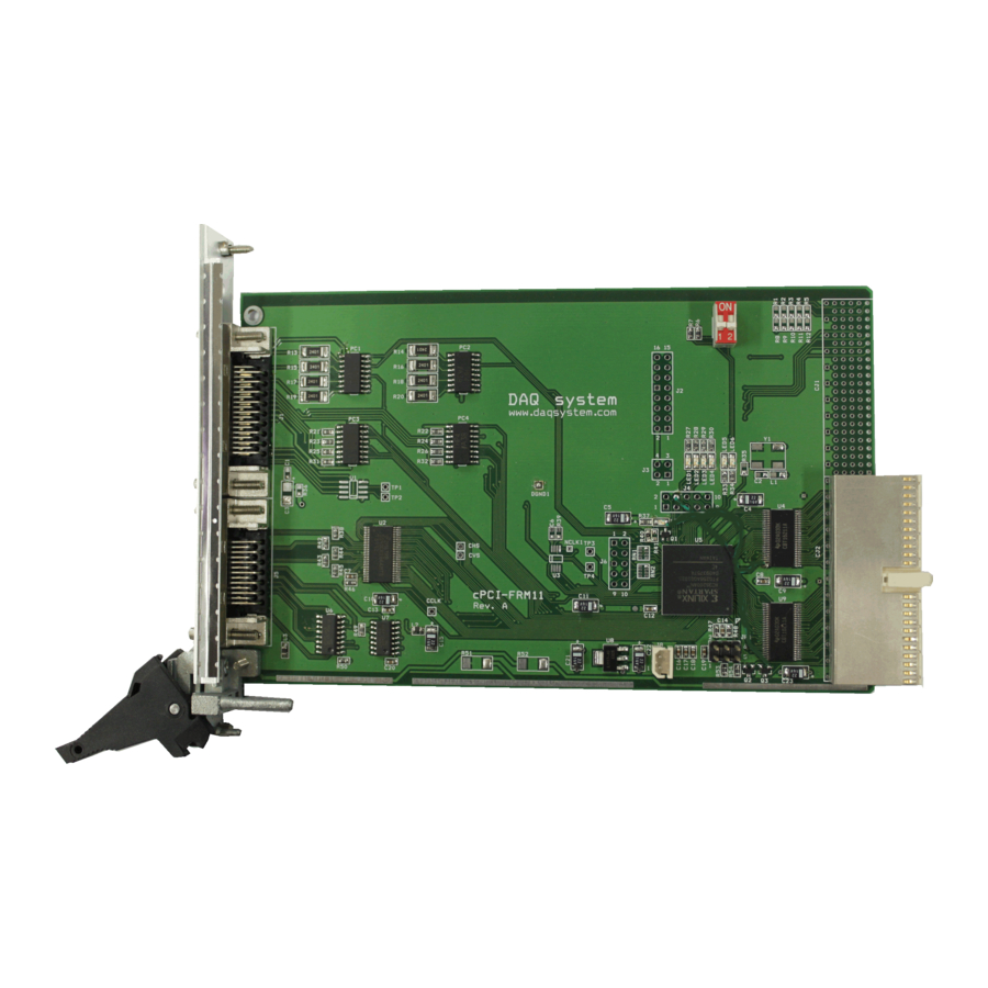
User’s Manual (Rev 1.1) 3. cPCI-FRM11 Board Description In this chapter, the primary functions of the cPCI-FRM11 board are described briefly. For more information, refer to the device specification. 3.1 PCB Layout [Figure 3-1. cPCI-FRM11 PCB Layout] The board has seven LEDs to indicate the operation status. - Page 7 User’s Manual (Rev 1.1) 3.2 Description of the functional blocks (1) FPGA : U5 All of the board functions are controlled by the Logic program of the FPGA. (2) LVDS : U4, U9 Receive Image frame through LVDS interface.
-
Page 8: Connector Pin-Out
User’s Manual (Rev 1.1) 3.3 Connector Pin-out The cPCI-FRM11 board is equipped with MDR 26 Pin connector for Camera Link connection and MDR 36 Pin connector for external I/O connection. Figure [4-2] shows the bracket of the board where J1 and J5 connector exist. - Page 9 Figure [4-3] shows the board‟s J1 connector pin-map. All of the pin functions are based on the Camera link standard, so please refer to the Camera link standard document for more description and information. [Figure 4-3. cPCI-FRM11 J1 Connector Pin-out] [Table 1. J1 Connector Description] Signal Name...
- Page 10 INPUT COMMON0 (FOR input 0,1,2,3) DIN3 INPUT 3 DIN2 INPUT 2 DIN1 INPUT 1 INPUT 0 DIN0 The cPCI-FRM11 board has eight-photo-coupler isolated digital inputs and eight equivalent outputs. Each is available from J1 connector. Figure [4-4] shows the isolated digital I/O circuits. http://www.daqsystem.com...
- Page 11 User’s Manual (Rev 1.1) [Photo-coupler Digital Input/Output] 2.4K DIN7..4 IN7..4 DIN_COM1 2.4K DIN3..0 IN3..0 DIN_COM0 < Photo coupler input> D O U T 3 ..0 DOUT_COM0 OUT3..0 D O U T 7 ..4 DOUT_COM1 OUT7..4 <Photo coupler output> [Figure 4-4. Photo-coupler Input/ Output circuit] The input resistance is 2.4KΩ(ohms) thus the flow current is about 5mA when 12V input is applied...
- Page 12 CC1- CC1+ CC2+ CC2- CC3- CC3+ CC4+ CC4- Inner shield Inner shield [Figure 4-5. cPCI-FRM11 J5 Connector Pin-out] [Table 1. J1 Connector Description] Signal Name Description Remark Inner Shield Cable shield Camera Control output 4- CC4- Refer to Figure 4-6...
- Page 13 Camera-link Cable. The cPCI-FRM11 board has four differential digital outputs. You use a Trigger out to be selected one of the four CC(Camera Control) in case of the Line Scan Camera. Each output is mapped by Digital output.
- Page 14 [Figure 4-6. Camera Control LVDS Digital Output Circuit] This picture below shows that a general input circuit is used at cPCI-FRM11 board. It is a serial input signal through Camera-link Cable. When serial input signal is used by general input, it is mapped by Digital input 8 and it can read a value of it.
- Page 15 User’s Manual (Rev 1.1) [Description of SW1] The cPCI-FRM11 board is designed of four maximum cPCI-FRM11 boards at the same time so as usable. Distribution of each board sets it up through 4 pin switch (SW1) in a board.
- Page 16 To install your cPCI-FRM11 board in your PC, follow the steps described in the document “How to install PCI DAQ Board” provided by DAQ System. If the document is missing, you can get it from www.daqsystem.com. The PCIe-FRM11 board is completely Plug & Play. There are no switches or jumpers to set.
- Page 17 User’s Manual (Rev 1.1) If new hardware is found, Wizard will ask you to install the corresponding driver. For installation of the driver, select the item “Install from a list or specific location (Advanced)” and click “Next” as in the figure.
- Page 18 User’s Manual (Rev 1.1) If the installation is completely finished, you confirm it in the following ways. http://www.daqsystem.com...
- Page 19 User’s Manual (Rev 1.1) Do the following steps to show up the “Device Manager” window. [My Computer -> properties -> Hardware -> Device Manager -> Multifunction Adaptors -> PCIe-FRM11] [Figure 4-1. Select “My computer”->”Properties”] [Figure 4-2. “System Properties” window-“Hardware” Tab]...
- Page 20 User’s Manual (Rev 1.1) [Figure 4-3. “Device Manager” window] If you can see the “PCIe-FRM11” (The cPCI-FRM11 uses a same driver with PCIe-FRM11 because of compatibility.) at Multifunction Adaptors, the driver installation is to have been over. (Check the red circle) Important Notice : After installation, you should re-boot the system for the proper operation.
-
Page 21: Sample Program
User’s Manual (Rev 1.1) 5. Sample Program DAQ system provides a sample program to make the user be familiar with the board operation and to make the program development easier. You can find the sample program in the CDROM accompanying with the board. - Page 22 User’s Manual (Rev 1.1) To run the sample application program, you need to use API, it is a form of client DLL. To compile the sample source to make its executable file, you have to use Import Library files and header files.
- Page 23 User’s Manual (Rev 1.1) (3) „Clear Serial Data’ button Press this button to clear the contents of the editor box. (4) „Start Timer’ button Press this button to start the timer. The sample program will read the UART data periodically.
-
Page 24: Test
User’s Manual (Rev 1.1) 6. Test 6.1 Receiving the image frame data In this chapter, the functional test will be explained to discriminate board mal-functions and for the user being familiar with the operation of the board. It is performed using the sample program “FrmTest.exe”. -
Page 25: Uart Tx/Rx Test
User’s Manual (Rev 1.1) Step 2 : Press the “Frame Read” button. Then data are displayed on editor box. Compare the contents of the editor box with the data of the Image Frame Simulator. Comparison can be performed using the “Save to” button. It saves the contents of the editor box to a file. -
Page 26: Appendix
User’s Manual (Rev 1.1) Appendix A.1 General Specification Specification General PCI Express Specification Revision 1.0 PCI Express 1x interface PCI Target and Master operation Camera Link interface specification Interface +5V Single Power operation Max 300mA under ... - Page 27 1. Specification of Camera Link Interface Standard for Digital Cameras and Frame Grabbers -- Camera Link committee 2. PCI Local Bus Specification Revision2.1 -- PCI Special Interest Group 3. How to install PCI DAQ Board -- DAQ system 4. AN201 How to build application using API -- DAQ system 5.
Need help?
Do you have a question about the cPCI-FRM11 and is the answer not in the manual?
Questions and answers